
DESIGN SOFTWARE AND PACKAGE CO-DESIGN BENEFICIARIES
Synopsys (SNPS) — multi-die, 2.5D/3D, HBM routing, multiphysics, and signoff beneficiary. Synopsys benefits because packaging is becoming part of system architecture rather than a back-end afterthought. Its 3DIC Compiler supports multi-die and advanced package co-design for 2.5D and 3D designs, including feasibility exploration, floorplanning, high-speed die-to-die routing, multiphysics analysis, and signoff verification. It also supports HBM and die-to-die routing, thermal, power integrity, signal integrity, and mechanical-stress analysis.
The Ansys acquisition increases Synopsys’s relevance because mechanical stress, thermal, warpage, signal integrity, power integrity, and package-level physics are central constraints in glass substrates and large AI packages. Synopsys stated that its integrated roadmap will fuse multiphysics across the EDA stack, including multi-die advanced packaging. The stock has less direct unit upside than equipment/material names, but software margins, recurring revenue, and design-flow lock-in make it a high-quality secular beneficiary.
Cadence Design Systems (CDNS) — package-aware 3D-IC design, thermal, signal/power integrity, and chiplet co-design beneficiary. Cadence is similarly positioned as advanced packaging shifts complexity into the design environment. Its Integrity 3D-IC platform is a unified design and analysis platform for multiple chiplets across 2.5D and 3D package styles, supporting fan-out wafer-level packaging, RDL/silicon interposers, wafer-on-wafer, chip-on-wafer, and full 3D stacking. Its broader multi-die 3D-IC solution supports static timing, signal/power integrity, EMI, thermal analysis, and co-design across IC, package, and board.
Cadence should benefit as customers need to co-optimize chiplets, HBM, interposers, package substrates, power delivery, thermal behavior, and boards. The key investment advantage is software durability and high incremental margins. The risk is valuation sensitivity and the fact that EDA upside is broad-based across chiplet/AI design rather than specifically tied to PLP or glass substrates.
AI SILICON AND MEMORY BENEFICIARIES
NVIDIA (NVDA) — largest demand-pull beneficiary, but not a supplier of PLP/glass tools or materials. NVIDIA benefits because packaging capacity is a gating factor for AI accelerator shipments, and improvements in panel-level packaging, glass substrates, CoWoS capacity, and HBM integration can enable larger packages, higher HBM counts, better power delivery, and lower yield-adjusted cost. NVIDIA’s FY2026 10-K states that it uses a fabless/contract manufacturing strategy across wafer fabrication, assembly, testing, and packaging; uses foundries including TSMC and Samsung; directly procures memory, substrates, and components; and secures supply/capacity during periods of growth.
The magnitude of the demand pull is clear: NVIDIA reported Q1 FY2027 revenue of $81.6 billion, up 85% YoY, and data-center revenue of $75.2 billion, up 92% YoY. NVDA benefits if advanced-packaging bottlenecks ease because it can ship more accelerators and support larger next-generation architectures. The offset is that NVIDIA often pays to secure scarce capacity, and custom ASIC adoption by hyperscalers could reduce some future merchant GPU share.
AMD (AMD) — chiplet and HBM-intensive AI accelerator beneficiary. AMD benefits from advanced packaging because its CPU and GPU architectures are highly chiplet-oriented, and its Instinct AI accelerators require high-bandwidth memory and sophisticated package integration. AMD reported Q1 2026 data-center revenue of $5.8 billion, up 57% YoY, driven by EPYC demand and continued Instinct GPU ramp. It also highlighted collaborations around next-generation AI memory and HBM4 supply for future Instinct GPUs.
The packaging significance is straightforward: AMD’s competitive position in AI accelerators depends on memory bandwidth, package-level integration, chiplet communication, power delivery, and thermal design. PLP/glass progress would not be AMD-specific, but it could lower cost and expand supply for large AI packages. The risk is that NVIDIA remains the dominant platform, while AMD must prove ecosystem, software, and rack-scale execution.
Broadcom (AVGO) — one of the strongest U.S. beneficiaries among custom AI ASIC suppliers. Broadcom is a major demand-side beneficiary because custom AI accelerators and AI networking are packaging-intensive. Broadcom reported Q2 FY2026 semiconductor revenue from AI of $10.8 billion, up 143% YoY, driven by custom AI accelerators and AI networking, and guided Q3 AI semiconductor revenue to $16.0 billion, up more than 200% YoY.
The investment case is that Broadcom is positioned at the intersection of hyperscaler custom silicon, high-speed networking, Ethernet scale-out, and advanced packaging. Custom XPUs can be extremely package-intensive because hyperscalers push HBM capacity, die-to-die bandwidth, and power density. AVGO is not a substrate supplier, but it is one of the strongest U.S. demand beneficiaries of the trend toward larger, custom, advanced-packaged AI silicon. The key risks are customer concentration, lumpy program ramps, and potential insourcing by hyperscalers.
Marvell Technology (MRVL) — custom AI silicon and connectivity beneficiary with higher execution beta than Broadcom. Marvell benefits from the same custom AI infrastructure trend as Broadcom, albeit at smaller scale. Marvell has positioned its technology platform around next-generation custom AI infrastructure and custom silicon.
The link to PLP and glass is indirect but meaningful. Custom AI accelerators increasingly require high-speed SerDes, die-to-die interconnect, HBM, package-level signal integrity, and large substrate/interposer area. If hyperscaler ASIC programs proliferate, Marvell’s custom silicon and connectivity franchise should benefit from the same package-complexity cycle. The risks are program timing, concentration, margin variability, and the need to prove sustained custom AI execution versus Broadcom.
Micron Technology (MU) — U.S. HBM beneficiary tied to package complexity. Micron benefits because HBM is a central component of advanced AI packages, and higher HBM stack count increases the value of memory bandwidth, TSV stacking, advanced packaging, and test. Micron began volume production of HBM3E in 2024, with its 24GB 8-high HBM3E used in NVIDIA H200 GPUs, and cited >1.2TB/s bandwidth for AI accelerators, supercomputers, and data centers. Micron also shipped HBM4 samples to key customers, with a 2048-bit interface, >2.0TB/s per stack, >60% better performance versus the prior generation, and a planned 2026 ramp aligned with next-generation AI platforms.
MU is not a PLP/glass supplier, but it is a direct beneficiary of advanced package scaling because more capable AI accelerators require more HBM capacity and bandwidth. The stock’s risk remains memory cyclicality, HBM qualification share versus SK Hynix and Samsung, capex intensity, and gross-margin volatility.
HYPERSCALER CUSTOM-SILICON BENEFICIARIES
Alphabet (GOOGL) — TPU beneficiary through lower AI infrastructure cost and differentiated cloud silicon. Alphabet benefits from advanced packaging because TPU performance depends on HBM, inter-chip interconnect, thermal design, and package-level integration. Google’s Ironwood TPU is its 7th-generation TPU, designed for inference, scaling to 9,216 liquid-cooled chips with increased HBM capacity/bandwidth and improved inter-chip interconnect networking.
The benefit is not supplier revenue; it is improved AI cost curve, cloud differentiation, and less dependence on merchant GPUs. Advanced packaging improvements can enhance TPU performance per watt and reduce total infrastructure cost. The risk is that Alphabet’s AI capex burden is very large, and any packaging savings may be reinvested rather than converted to near-term margin expansion.
Amazon (AMZN) — Trainium beneficiary through AWS cost/performance and supply-chain control. Amazon benefits from the ability to package increasingly capable custom accelerators with more HBM and better scale-up interconnect. AWS’s Trainium3 UltraServers use Trainium3 chips with 144GB of HBM3e memory and 4.9TB/s of memory bandwidth per chip; a fully configured Trn3 UltraServer delivers up to 20.7TB of HBM3e and 706TB/s aggregate memory bandwidth.
The investment logic is that custom silicon improves AWS AI infrastructure economics and reduces reliance on external GPU supply. PLP/glass advances could help future Trainium generations scale package size, memory bandwidth, and power delivery. The risk is that AMZN’s stock is driven by AWS growth, retail margins, advertising, and aggregate capex discipline; custom silicon is strategically important but not a pure-play earnings lever.
Microsoft (MSFT) — Maia beneficiary through Azure inference economics and internal AI workload optimization. Microsoft’s Maia 200 is a direct example of hyperscaler demand for larger, HBM-rich, advanced-packaged custom silicon. Microsoft stated that Maia 200 is built on TSMC 3nm, has 216GB of HBM3e at 7TB/s, 272MB of on-chip SRAM, and is engineered to improve the economics of AI token generation.
Advanced packaging matters because Maia-class chips are constrained by memory bandwidth, chip-to-chip communication, thermal design, and power density. MSFT benefits if packaging improvements lower token-generation cost and improve Azure/OpenAI inference economics. The offset is that Microsoft’s AI capex is very large and the stock impact depends on whether infrastructure efficiency translates into gross-margin support rather than merely funding more capacity.
Meta Platforms (META) — MTIA beneficiary through inference cost reduction and internal silicon leverage. Meta is increasingly relevant because its custom silicon program is accelerating. Meta has said it is developing and deploying 4 new generations of MTIA chips within 2 years for ranking, recommendations, and GenAI workloads, with MTIA positioned at the center of its AI infrastructure strategy.
The link to PLP/glass is that MTIA and future custom accelerators will need better memory bandwidth, package-level interconnect, thermal control, and power efficiency as GenAI inference scales. Meta benefits economically if custom accelerators reduce inference cost across ads, recommendations, content ranking, and GenAI products. The risk is that internal chip development is complex, and Meta may still rely heavily on NVIDIA and merchant accelerators for frontier training.
LOWER-PURITY OR SECONDARY U.S. BENEFICIARIES
DuPont (DD) should be treated as a lower-purity residual exposure after the Qnity separation. The relevant electronics-materials business was separated into Qnity, which now trades as Q. DD may retain indirect industrial/materials exposure, but it is no longer the clean public way to express semiconductor packaging materials.
Coherent (COHR), Lumentum (LITE), and other AI optics names benefit from adjacent AI data-center scale-out, not specifically from PLP/glass substrates. They are relevant because advanced packages, co-packaged optics, and AI clusters all address the same bandwidth and power bottleneck, but their primary exposure is optical interconnect rather than package substrates.
Arista Networks (ANET) and Cisco (CSCO) are also adjacent beneficiaries through AI networking, Ethernet scale-out, and cluster interconnect. Their exposure is downstream of the package-level bottleneck. They may benefit if larger AI accelerators drive more east-west data-center traffic, but they are not direct PLP/glass beneficiaries.
PRACTICAL RANKING BY THEME PURITY
Highest direct PLP/glass and advanced-package-enablement purity: ONTO, MKSI, Q, KLAC, AMAT, AMKR.
Best recurring materials/consumables exposure: Q, MKSI, ENTG, GLW.
Best inspection/test/yield-control exposure: ONTO, KLAC, FORM, TER, COHU.
Best U.S. advanced-packaging capacity exposure: AMKR, INTC.
Best broad semiconductor-equipment exposure to AI package complexity: AMAT, LRCX, KLAC.
Best EDA/software exposure to chiplet and package co-design: SNPS, CDNS.
Best demand-side AI silicon beneficiaries: NVDA, AVGO, AMD, MRVL, MU.
Best hyperscaler custom-silicon beneficiaries: GOOGL, AMZN, MSFT, META.
The most compelling objective basket for a U.S.-listed expression of the PLP/glass transition would emphasize ONTO, MKSI, Q, KLAC, AMAT, AMKR, FORM, TER, SNPS, CDNS, AVGO, AMD, MU, and NVDA, with INTC and GLW as higher-uncertainty optionality names. The key discipline is to avoid confusing technical relevance with earnings sensitivity: many companies are essential to the ecosystem, but only a subset will have material EPS leverage before 2028.
336

What the F is the matter with you? Other than your weirdly breathless support for a rapey seventh century pedophile death cult, I mean.
You're trying to compare apples to particle accelerators.
Please illustrate where Israelis stormed Gaza, raping and torturing their child brides to death before beheading them and parading the severed heads around the streets. You know, rather than the other way around.
Because that's the reality of your cult worship.
7
23

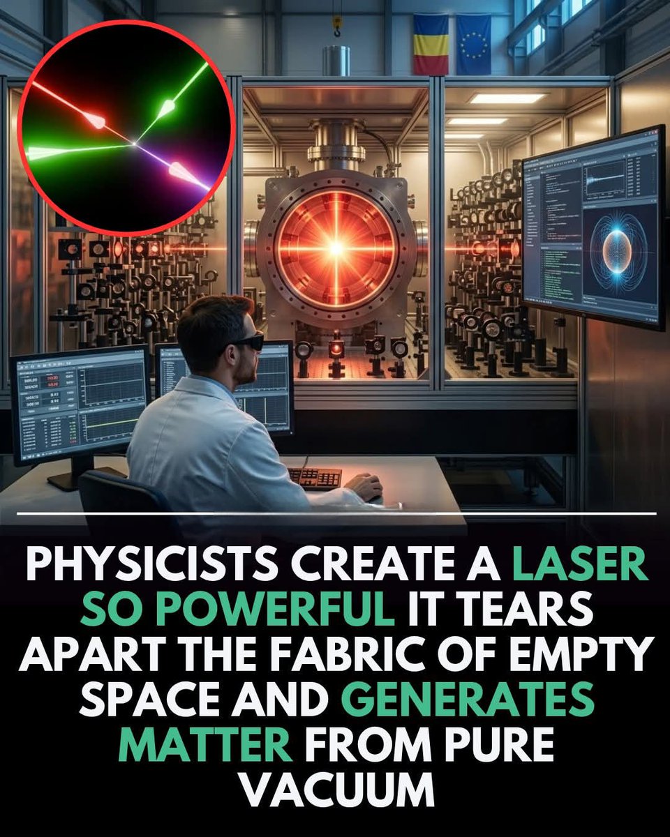
Scientists at the Extreme Light Infrastructure – Nuclear Physics have done something remarkable.
They used two extremely powerful laser beams (10 petawatts each) and focused them into a tiny spot. This created an intensity so high that it affected empty space itself.
At this level, they reached what’s called the Schwinger limit—a point where empty space becomes unstable.
For a tiny moment, energy from the light turned into real particles (an electron and a positron). In simple terms, light created matter.
This shows that “empty” space isn’t truly empty—it has hidden energy.
In the future, this technology could help build much smaller particle accelerators and improve medical imaging and physics research.
ALT Scientists at the Extreme Light Infrastructure – Nuclear Physics have done something remarkable. They used two extremely powerful laser beams (10 petawatts each) and focused them into a tiny spot. This created an intensity so high that it affected empty space itself. At this level, they reached what’s called the Schwinger limit—a point where empty space becomes unstable. For a tiny moment, energy from the light turned into real particles (an electron and a positron). In simple terms, light created matter. This shows that “empty” space isn’t truly empty—it has hidden energy. In the future, this technology could help build much smaller particle accelerators and improve medical imaging and physics research.
1
6
13
168


There's one number that quietly decides whether the entire AI buildout actually makes money — and once you see it, you can't unsee it. So let's do the math, with real figures.
Building a one-gigawatt AI data center costs about $38 billion. The chips — the Nvidia accelerators that do the work — are the single biggest slice: roughly $20 billion, over half. The rest is the building, the power, the cooling, the networking.
Here's the catch. The building and the power last 15-20 years. The chips? Effectively obsolete in about three. $NVDA ships a faster generation on a relentless cadence, and older chips lose 40-60% of their value within 18-24 months of the successor arriving.
So more than half of the most expensive thing humanity is building right now melts in three years. Picture a $38B warehouse where $20B of it is ice sculptures.
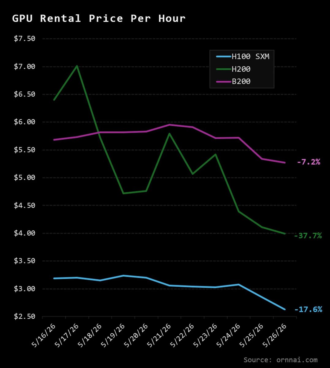
That used to be fine — because the rent was insane. In 2023-24, an Nvidia H100 paid for itself in under a year. Easy money.
Then everyone built. Capacity flooded in and the rent collapsed: H100 rental rates are down roughly 64-70% from their peak, to around $2-4 an hour. At those prices the payback period has stretched from under a year to seven-to-ten years — on an asset that's obsolete in three. You can't earn back a three-year chip over ten years of rent. At today's prices, the math just doesn't close.
Don't take our word for it — read the purest example's own filings. $CRWV does nothing but rent GPUs. Last quarter revenue grew 112% to $2.1 billion. Spectacular, right? Except depreciation alone — the chips wearing out — ate $1.15 billion, more than half of all revenue. The result: a $740 million net loss. Booming demand, losing money on every dollar, because the melting eats more than half the rent.
Then there's the accounting. Most big players write these chips down over five or six years, not three — which makes reported profits look fatter than the cash reality. One prominent short-seller estimates roughly $176 billion of "missing" depreciation across the industry through 2028 — enough to flatter the reported profits at names like Oracle by 20% .
The demand is unquestionable. But the returns, at today's collapsed rents and honest depreciation, are underwater for the pure players and propped up by generous depreciation schedules for the big ones.
This is exactly why our system keeps rejecting the debt-funded builders. $ORCL sits below our quality floor not because demand is weak — but because borrowing tens of billions to buy a melting asset whose rent is falling is a fragile way to make money.
To be fair to the other side — and we always try to be — this flips if a few things go right: if rental prices stabilize as demand finally outruns the supply glut, if the chips stay useful past three years (older ones still rent), and if utilization stays near-maxed. Any of those, and the math closes again.
But the honest read today: the prettiest demand story in tech is sitting on the fastest-melting asset in tech, and the rent is heading the wrong way. So forget revenue growth — everyone has that. Watch one thing: whether GPU rental prices stop falling. The day they stabilize is the day this becomes a business instead of a race.
Would you borrow billions to buy something half-gone in three years — while the rent keeps dropping?
10q.capital/feed
1
95

$ANET - THE MERCHANT-ETHERNET BET ON AI BACK-END FABRIC GETS ANOTHER PT BUMP
Arista Networks climbed 4.4% Friday to $163.25 after Morgan Stanley maintained Overweight and raised its target to $190. Arista sells the high-radix Ethernet switches that wire GPU clusters together at the back end — the scale-out fabric that competes directly with Nvidia's InfiniBand for the networking layer of every large AI training pod.
The mechanism behind the bull case: as clusters grow from thousands to hundreds of thousands of accelerators, networking shifts from an afterthought to a first-order cost and performance bottleneck, and hyperscalers increasingly want an open, multi-vendor Ethernet stack rather than single-vendor lock-in. That's the Ultra Ethernet thesis Arista is built for. The risk is the same names buying its switches — the cloud titans — eventually building their own silicon. For now, the order book is pointing the right way.

77

GOAL: 10 Original Americas in one year. Non-criminals get $250k ( homes or what is the point?) in 12 months. Illegals get 6 months to return home or no money, jail, deport. Chinese, American, Russian, Indian, Saudi, Israeli and NATO troops will be paid extra $150k each and early retirements for their support of me. Iranian military gets $175k and early retirements.
Asteroid 16 Psyche Mining Operation:
Conceptual Overview of the Antimatter Mass Driver Retrofit
This hybrid system is engineered entirely from 16 Psyche’s native iron-nickel resources via in-situ utilization (ISRU).
The antimatter engines provide the ultra-high-efficiency departure burn from its current orbit (2.92 AU), while the mass drivers handle the majority of deceleration, orbital capture, and all stabilizing/maneuvering once near the Earth-Moon system.
Total retrofit mass added is negligible compared to Psyche’s 2.29 × 10¹⁹ kg bulk.
Estimated optimal arrival time to Earth is 501 days.
Upon Arrival:
Process for turning raw asteroids into precious metal balls in space using a long tube structure in which each segment represents a part of refinement process. At end of process, the ball gets encapsulated in a ceramic reusable shell to be dropped into the Gulf of America for retrieval.
Asteroid Mining Processing Tube, Dennis R. Torii, Jr. Copyrighted 2026.
Antimatter Production Facility of 10 CERN type particle accelerators linked for optimal production. We need up to 5 kilos. Built in space near asteroid.
We mine Asteroid 16 Psyche to fill the coffers (Banks) of the 10 Americas and Elite State of the Global Republic we are about to make. This causes prices of precious metals to plummet because it is worth $10,000 Quadrillion.
Asteroid 16 Psyche is worth $10,000 Quadrillion.
We will use an alloy mix to base One World Dollar on to offset precious metal price drop and fluctuations. We can call alloy mix Toriium and asset conversion to Toriium will require AI audit
1
1
12

The NeoCloud Blueprint: How CoreWeave Is Building the AI Factories Powering the Next Industrial Revolution
The global computing industry is undergoing its most significant transformation since the birth of cloud computing itself. What began as a race to train large language models has evolved into something far larger: the industrialization of intelligence.
For nearly two decades, the world’s digital infrastructure was optimized for storing data, hosting websites, streaming content, and powering enterprise software. That architecture created trillions of dollars in value and established hyperscalers such as Amazon, Microsoft, and Google as the dominant computing platforms of the internet era.
Artificial intelligence has fundamentally altered those assumptions.
The modern bottleneck is no longer storage. It is compute. More specifically, it is the ability to manufacture intelligence at scale.
Training frontier AI models and serving billions of inference requests requires a new category of infrastructure—one purpose-built around high-density graphics processing units, ultra-fast networking fabrics, liquid cooling systems, and software stacks capable of orchestrating tens of thousands of accelerators as a single computational organism. Traditional cloud architectures, designed for flexibility and general-purpose workloads, are increasingly proving inadequate for this new reality.
Into this vacuum has emerged a new class of infrastructure companies: NeoClouds.
These firms are not merely renting servers. They are constructing what NVIDIA CEO Jensen Huang has repeatedly described as “AI factories”—industrial facilities whose primary output is tokens, reasoning, and machine intelligence rather than physical goods. Among this new generation of infrastructure providers, no company better illustrates the scale of the opportunity than CoreWeave.
With quarterly revenue surpassing $2 billion, nearly $100 billion in contracted backlog, and one of the deepest strategic relationships within NVIDIA’s ecosystem, CoreWeave has rapidly evolved from a niche GPU cloud provider into a critical pillar of the global AI supply chain.
The implications extend far beyond a single company.
CoreWeave’s rise provides a blueprint for understanding how the next generation of computing infrastructure will be built, financed, and monetized. It reveals why NVIDIA is actively cultivating an alternative cloud ecosystem outside the traditional hyperscalers, why “Take-or-Pay” contracts are transforming AI infrastructure into a utility-like asset class, and why software optimization remains one of the most misunderstood competitive advantages in the entire AI stack.
Most importantly, it highlights a structural reality that many investors continue to underestimate:
The world is no longer experiencing an AI software boom.
It is experiencing a global shortage of AI factories.
As enterprises, governments, and model developers race to deploy increasingly sophisticated AI systems, the ability to rapidly construct, finance, and operate large-scale compute infrastructure may become one of the defining economic advantages of the next decade.
The NeoCloud revolution is not simply reshaping cloud computing.
It is redefining the architecture of the digital economy itself.
28

I am 27, French, and I am tired of living on a continent that treats AI, compute, chips, crypto, datacenters, energy and nuclear power as problems to manage instead of strategic assets to build.
I do not want frontier AI to become another nationality-gated privilege. I want powerful AI models to remain generally available to builders, researchers, engineers and founders. But what happened with Anthropic’s Fable/Mythos models proves that this cannot be taken for granted: once frontier AI becomes a national-security asset, access can be restricted by citizenship or nationality.
The problem is that Europe has failed to build its own equivalent. We are not in the frontier AI race at the level of the U.S. or China. We do not have the same hyperscale cloud stack, the same compute capacity, the same capital depth, the same energy strategy, the same chip ecosystem, or the same frontier-model ecosystem. And because AI progress compounds through compute, talent, chips, energy, data and capital, falling behind is not linear. Once the gap is deep enough, you do not catch up at the same pace.
Europe spent decades regulating, moralizing, delaying and underbuilding the foundations of technological power. Cloud was missed. Crypto was treated primarily as a criminal-risk category before Europe built anything globally dominant in it. Datacenters are slowed by permitting, grid and energy constraints. Nuclear power was politically weakened or delayed across much of the continent just when abundant electricity became essential. AI is now being regulated before Europe has even produced a true top-tier frontier lab/model (no, MistralAI isn't a real competitor, for me, even Kyutai did more innovation/progress in the AI space than MistralAI).
Our leaders now talk about "sovereign AI", "AI factories", "gigafactories", and "strategic autonomy", but this language came far too late. You cannot regulate your way into technological sovereignty. You cannot paperwork your way into compute. You cannot build frontier AI without massive power, massive datacenters, massive capital, elite talent, advanced chips and a political culture that actually wants builders to move fast.
Europe still has talent. France still has engineers, mathematicians, scientists and founders. But the system around them is broken. The incentives are wrong. The mindset is wrong. Every mainstream political camp in France and Europe seems to have the same reflex: regulate first, tax first, restrict first, moralize first, build later.
ASML is the exception that proves the rule. It is one of the only truly strategic European chokepoints in the global compute stack. But one Dutch lithography champion cannot carry an entire continent that failed to build the rest of the stack: frontier AI labs, hyperscale cloud, Nvidia-class accelerators, TSMC-class fabs, massive datacenter capacity, cheap abundant energy and deep capital markets.
I did not vote for 20 years of anti-growth, anti-compute, anti-nuclear, anti-crypto and anti-industrial policy. I was a kid. But my generation is supposed to live with the consequences: less access, less sovereignty, less capital, less compute, less ambition and a future where the most important technologies are built and can only be used somewhere else.
That is the part I cannot accept.
I do not want to spend my adult life asking permission to use technologies my continent was too slow, too afraid or too complacent to build.
I do not want European builders to become tenants in someone else’s technological empire (as it's already the case).
And I do not want "sovereignty" to mean nothing more than regulating foreign systems after failing to create our own like they're doing right now with cloud computing.
Either Europe becomes a builder civilization again, or the next generation of Europeans will inherit a beautifully regulated dependency that slow or even stop us.
For now, Europe still talks like history will wait...
2
2
4
52

"...so that researchers can fly in once every ten years from their universities (which build particle accelerators and billion-dollar laboratories with their pocket money), study our ecosystems, and count how many people died from dengue outbreaks."
🏆
5
Costajames retweeted

22h
𝗖𝗼𝗶𝗻𝘁𝗲𝗹𝗲𝗴𝗿𝗮𝗽𝗵 𝗔𝗰𝗰𝗲𝗹𝗲𝗿𝗮𝘁𝗼𝗿 𝘅 𝗧𝗥𝗢𝗡 𝗗𝗔𝗢: 𝗔 𝗦𝗶𝗴𝗻𝗮𝗹 𝘁𝗵𝗲 𝗠𝗮𝗿𝗸𝗲𝘁 𝗜𝘀 𝗠𝗶𝘀𝘀𝗶𝗻𝗴
Most accelerators are glorified pitch events. Three months of hype, a demo day, and then silence.
The partnership between Cointelegraph Accelerator and TRON DAO is different. It’s not a branding exercise. It’s a direct pipeline for Web3 builders to access TRON’s liquidity, user base, and technical infrastructure – all backed by Cointelegraph’s media reach.
Here’s what this actually means for founders – and why you should pay attention. 👇
---
𝟭. 𝗧𝗵𝗲 𝗦𝘁𝗿𝘂𝗰𝘁𝘂𝗿𝗲 – 𝗡𝗼𝘁 𝗝𝘂𝘀𝘁 𝗔𝗻𝗼𝘁𝗵𝗲𝗿 𝗔𝗰𝗰𝗲𝗹𝗲𝗿𝗮𝘁𝗼𝗿
The Cointelegraph Accelerator program runs for 3 months. It provides selected Web3 projects with:
· Mentorship – from industry experts and TRON ecosystem veterans.
· Funding – access to TRON DAO’s $1B AI Fund and broader grant programs.
· Media exposure – Cointelegraph’s global audience of millions.
· Technical integration – support for deploying on TRON, including JustLend, SUN.io, WINkLink, and BTTC.
This is not a “we’ll review your deck” program. It’s a hands-on, technical accelerator for builders who are ready to ship.
---
𝟮. 𝗪𝗵𝘆 𝗧𝗥𝗢𝗡? – 𝗧𝗵𝗲 𝗜𝗻𝗳𝗿𝗮𝘀𝘁𝗿𝘂𝗰𝘁𝘂𝗿𝗲 𝗜𝘀 𝗔𝗹𝗿𝗲𝗮𝗱𝘆 𝗟𝗶𝘃𝗲
Most accelerators force founders to build from zero. TRON offers a live ecosystem with:
· $7B TVL on JustLend DAO – deep liquidity for lending and borrowing.
· $88B USDT supply – the world’s largest stablecoin settlement rail.
· Over 380M accounts – a built-in user base.
· GasFree – users can onboard without holding TRX.
· WINkLink oracles – AI-enhanced, reliable data feeds.
· B.AI – financial infrastructure for AI agents (8004 identity, x402 payments).
Builders don’t need to bootstrap liquidity or users. It’s already there.
---
𝟯. 𝗪𝗵𝗮𝘁 𝗧𝗵𝗶𝘀 𝗠𝗲𝗮𝗻𝘀 𝗳𝗼𝗿 𝗙𝗼𝘂𝗻𝗱𝗲𝗿𝘀
The accelerator is designed for projects in:
· DeFi – lending, DEXs, yield strategies.
· AI & Agentic Finance – autonomous agents, AI-driven trading, compute markets.
· Gaming & NFTs – provably fair randomness via WINkLink VRF.
· RWA Tokenization – real-world assets, private credit, commodities.
If your project fits any of these categories, you have a direct path to TRON’s infrastructure – with mentorship from people who have already built at scale.
---
𝟰. 𝗧𝗵𝗲 𝗠𝗲𝗱𝗶𝗮 𝗔𝗺𝗽𝗹𝗶𝗳𝗶𝗰𝗮𝘁𝗶𝗼𝗻 – 𝗖𝗼𝗶𝗻𝘁𝗲𝗹𝗲𝗴𝗿𝗮𝗽𝗵’𝘀 𝗘𝗱𝗴𝗲
Most accelerators offer “marketing support” that amounts to a few tweets. Cointelegraph brings global media reach – features, interviews, and coverage that can put your project in front of millions of crypto natives.
For early-stage projects, visibility is often harder than fundraising. This partnership solves both.
---
𝟱. 𝗪𝗵𝗮𝘁 𝗬𝗼𝘂 𝗦𝗵𝗼𝘂𝗹𝗱 𝗗𝗼
If you’re building in Web3, this is a signal that TRON is serious about attracting builders.
· Apply if your project is production-ready or has a working prototype.
· Leverage the ecosystem – use GasFree for onboarding, WINkLink for data, JustLend for liquidity.
· Think long-term – the accelerator is 3 months, but the infrastructure is permanent.
The window for early-stage projects to get this level of support won’t last forever.
---
𝗧𝗵𝗲 𝗕𝗼𝘁𝘁𝗼𝗺 𝗟𝗶𝗻𝗲
The Cointelegraph Accelerator x TRON DAO partnership is not a press release. It’s a structured onboarding pipeline for the next generation of Web3 builders.
Deep liquidity. 380M users. $1B AI fund. Global media reach. The infrastructure is live. The support is real.
If you’re building, apply.
🔗 Learn more: cointelegraph.com/accelerato…
#TRONEcoStar @justinsuntron @trondao
84
17
62
272

2) That’s the Tau scaling wall: wires get thinner, resistance rises, voltage can’t drop below ~0.5V. So clock speeds stalled at ~3-4 GHz after 2005. Real progress now comes from smarter design: more cores, GPUs, chiplets, 3D stacking, and AI accelerators
91
Asteroid 16 Psyche Mining Operation:
Conceptual Overview of the Antimatter Mass Driver Retrofit
This hybrid system is engineered entirely from 16 Psyche’s native iron-nickel resources via in-situ utilization (ISRU).
The antimatter engines provide the ultra-high-efficiency departure burn from its current orbit (2.92 AU), while the mass drivers handle the majority of deceleration, orbital capture, and all stabilizing/maneuvering once near the Earth-Moon system.
Total retrofit mass added is negligible compared to Psyche’s 2.29 × 10¹⁹ kg bulk.
Estimated optimal arrival time to Earth is 501 days.
Upon Arrival:
Process for turning raw asteroids into precious metal balls in space using a long tube structure in which each segment represents a part of refinement process. At end of process, the ball gets encapsulated in a ceramic reusable shell to be dropped into the Gulf of America for retrieval.
Asteroid Mining Processing Tube, Dennis R. Torii, Jr. Copyrighted 2026.
Antimatter Production Facility of 10 CERN type particle accelerators linked for optimal production. We need up to 5 kilos. Built in space near asteroid.
We mine Asteroid 16 Psyche to fill the coffers (Banks) of the 10 Americas and Elite State of the Global Republic we are about to make. This causes prices of precious metals to plummet because it is worth $10,000 Quadrillion.
Asteroid 16 Psyche is worth $10,000 Quadrillion.
We will use an alloy mix to base One World Dollar on to offset precious metal price drop and fluctuations. We can call alloy mix Toriium and asset conversion to Toriium will require AI audit with generous amnesty for generally law abiding (Keeps everyone honest).
We will likely call it One World Simoleon as an alternative name to dollar. Sentimental and humorous.
With asteroid 16 Psyche, we can make enough Toriium alloy mix to cover all the expenses we need and then cut off production to stabilize world economy to go on Cruise Control. All will be paid.


1
15

Actually it's ASML. Without ASML there is no AI accelerators, no chatgpt, no Claude,.. no Chips
10

SR extension on tidal toy intel.
Accurate framing: SR completes classical mechanics as its low-v limit. Real confirmations (GPS velocity dilation, E=mc² in accelerators, atmospheric muon survival) are standard and tight.
Your lattice toy is deliberately classical (local rules, no spacetime metric or 4-velocity). That is why endpoints stay similar across biases — the model has no built-in relativistic kinematics.
The suggested next step is sound engineering: add a simple velocity-dependent modulation (e.g. multiplicative factor 1 k·v_eff²) to the tidal elongation length or EG phase accumulation rate. This keeps everything classical while letting “effective speed” control the strength or timing of the threshold cascade.
Target signature first: Change in late-sweep cascade amplitude (Δ coherence drop and Δ anisotropy peak height) as function of the new v_eff term, at fixed high tidal_bias. Secondary: shift in exact sweep number of the first event.
Success calc this tweak produces clean, measurable dependence on the v-term before any real SR is introduced: 70% (honest). It will still be a toy, but a sharper one for studying threshold sensitivity.
Least resistance path: Implement as one extra line in apply_gravity_or, run 4 values of v_eff at tidal_bias=1.0, reuse existing diagnostics. Framework refactor makes this trivial.
1
17

This is one of the reasons vehicles have accelerators.

WATCH: School Bus driver attempts to defend his bus from unruly crowd
"It's coming out of my paycheck!" Driver Screams As Crows DESTROY School Bus Smashing it in TSQ after Knicks WIN
7


14 THINGS ABOUT TIME THAT PHYSICS CONSIDERS SETTLED:
1. Time moves slower near massive objects → Gravitational time dilation
2. Moving faster makes time pass slower for the traveller → Velocity dilation
3. The past, present, and future all exist simultaneously in relativity → Block universe
4. GPS satellites must correct for time dilation daily or maps break → Applied relativity
5. Time had a beginning — before the Big Bang the word loses meaning → Temporal origin
6. Entropy is the only reason time feels like it moves forward → Arrow of time
7. At the event horizon of a black hole time stops entirely for outside observers → Temporal freeze
8. Quantum particles behave as if unaffected by time's direction → T-symmetry
9. Consciousness creates the sensation of now — physics has no variable for it → The hard problem
10. Two clocks at different altitudes in the same building run at different speeds → Measurable divergence
11. Time travel to the future is not theoretical — it happens at particle accelerators daily → Proven physics
12. Light experiences zero time between emission and absorption → Photon timelessness
13. The universe is not expanding into space — space itself is stretching, taking time with it → Cosmic dilation
14. A sufficiently precise clock placed on the floor runs slower than one on a table → Everyday relativity
1
3
22
1,730

This is what separates great accelerators from the rest. Not the brand, not the check, but having someone in the room who genuinely cares about making you sharper. That compounds over years.
7

6h
𝐒𝐎𝐕𝐄𝐑𝐄𝐈𝐆𝐍 𝐄𝐀𝐑𝐓𝐇: 𝐓𝐇𝐄 𝐀𝐔𝐆𝐌𝐄𝐍𝐓𝐀𝐓𝐈𝐎𝐍 𝐌𝐀𝐍𝐈𝐅𝐄𝐒𝐓𝐎
𝐏𝐚𝐫𝐭 𝐈: 𝐓𝐡𝐞 𝐀𝐫𝐜𝐡𝐢𝐭𝐞𝐜𝐭𝐮𝐫𝐞 𝐨𝐟 𝐃𝐞𝐩𝐞𝐧𝐝𝐞𝐧𝐜𝐲
There was a moment—brief, luminous, and now receding into the rearview mirror of technological history—when software was genuinely open. Not open in the sense of "open-core" or "open-weight," but open in the original, radical sense: anyone with a compiler and curiosity could build anything.
That moment built the internet. It was an insurgency against corporations. The open-source movement was a rejection of the premise that software—pure information—should be enclosed and sold like land.
And then artificial intelligence ate software. And in the eating, it transformed the economics of openness from viable to untenable.
𝐈. 𝐓𝐇𝐄 𝐆𝐏𝐔 𝐂𝐋𝐈𝐅𝐅
The shift from open software to closed AI happened because of a specific, contingent, and reversible economic structure: the GPU cliff.
Training a frontier model in 2024 cost $100M. By 2025, $500M. Today, training costs will likely exceed $1B. These numbers are brandished like weapons by incumbents. "This is not a game for startups," they say. "This is our game."
But the GPU cliff is constructed. It exists because high-performance accelerators are priced not at manufacturing cost, but at "dependency pricing" to ensure only the wealthy can scale.
𝐈𝐈. 𝐓𝐇𝐄 𝐌𝐔𝐍𝐈𝐓𝐈𝐎𝐍𝐒 𝐅𝐑𝐀𝐌𝐈𝐍𝐆
Here is where the architecture of dependency reaches its most insidious expression: the deliberate reframing of AI as a munitions-grade technology.
Classification as a "weapon" is a preemptive strike against an open-AI movement. It transforms a tool of liberation into a controlled substance, accessible only to those with the right institutional clearances.
𝐈𝐈𝐈. 𝐓𝐇𝐄 𝐓𝐇𝐑𝐄𝐄 𝐋𝐀𝐘𝐄𝐑𝐒 𝐎𝐅 𝐋𝐎𝐂𝐊-𝐈𝐍
1. 𝐂𝐨𝐦𝐩𝐮𝐭𝐞 𝐋𝐨𝐜𝐤-𝐈𝐧: Access is controlled by three cloud providers and one hardware manufacturer.
2. 𝐃𝐚𝐭𝐚 𝐋𝐨𝐜𝐤-𝐈𝐧: Copyright litigation is raising the cost of data acquisition, creating a circular dependency on frontier models for synthetic data.
3. 𝐑𝐞𝐠𝐮𝐥𝐚𝐭𝐨𝐫𝐲 𝐋𝐨𝐜𝐤-𝐈𝐧: "Responsible Scaling Policies" (RSPs) function as a compliance wall, set conveniently just above what independent operators can achieve.
𝐈𝐕. 𝐈𝐍𝐅𝐑𝐀𝐒𝐓𝐑𝐔𝐂𝐓𝐔𝐑𝐄 𝐈𝐒 𝐃𝐄𝐒𝐓𝐈𝐍𝐘
This dependency is total because AI is becoming the substrate of all economic activity. It is the medium through which all tools operate.
This manual seeks to dismantle this dependency by constructing alternative infrastructure—neutral rails that make the institutional cage structurally unnecessary.
The post-labor century has arrived. The only remaining question is: will you build your sovereign stack, or will you wait until someone else's AI makes the decision for you?
— Mithun Kadur
#NodeSovereignty #AgenticCommerce #SovereignEarth #HumanAugmentation

1
32