
Et donc nous devons accepter leur propagande pro Ukraine et ils osent parler de liberté d expression et de démocratie interdire la parole aux aurntres c est de la dictature cette UE et les responsables de celle-ci sont en réalité lex3 reich loiseau le goebels de macron et uvdl
1
2
24


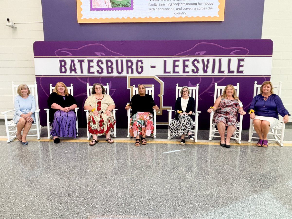
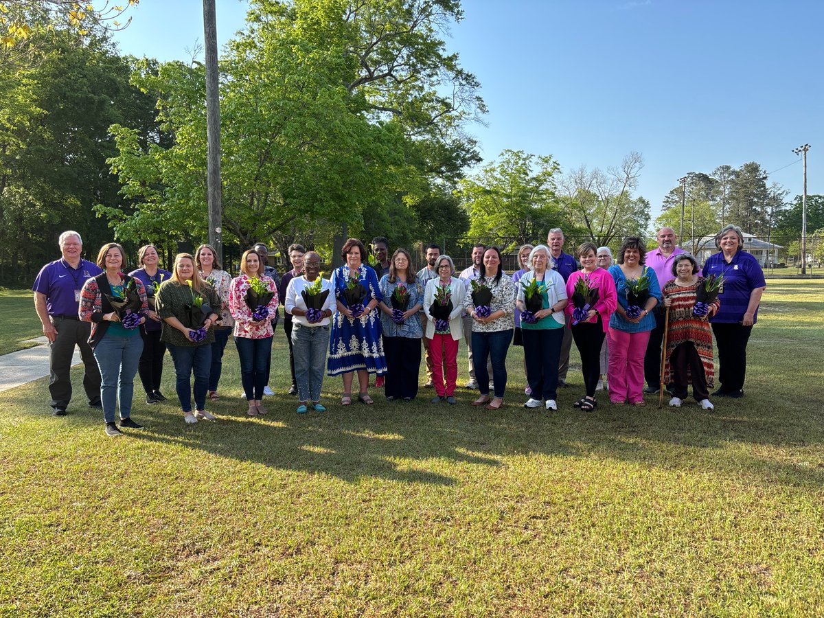
On Tuesday, #lex3 recognized the members of our 2026 Retiree Class with a reception held in the lobby of the new BLHS gym. This year, 10 individuals are retiring after contributing a total of 229.5 years of service to our district. Read more here: lex3.org/article/2873672
2
66

Apr 18
As I read the MATCH Act and all the commentary on the subject of DUVi lithography restrictions, it's helpful to understand that the said "loophole"—multipatterning—is a fab production method dating back nearly 2 decades.
2008: Intel 45nm Logic used dedicated gate & cut masks, the first known use of multi-patterning lithography where a single layer is accomplished with 2 mask exposures.
2011: TSMC others 20nm Logic used Litho-Etch Litho-Etch (LELE) multipatterning with hard mask memorization for 64p metal.
2012: Samsung 20nm DRAM used Self-Aligned Double Patterning (SADP) cut mask for critical layers; later, this was applied to logic gate fin patterning, and eventually SAQP became mainstream across all advanced chip patterning.
2018: TSMC 7nm logic, before EUV source power hit 250W, 7nm production had already ramped using immersion LEx3-4 for contact, metal and via layers.
On this last point, up until 2018, when the first commercially viable EUV systems were shipped (NXE:3400B), the 7nm plan was to use immersion lithography with the NXT:2000i system. The only reason the plan changed was the magic number at the time, 250W. This was the source power that made EUV cheaper than 4-pass immersion.
2
5
65
5,335
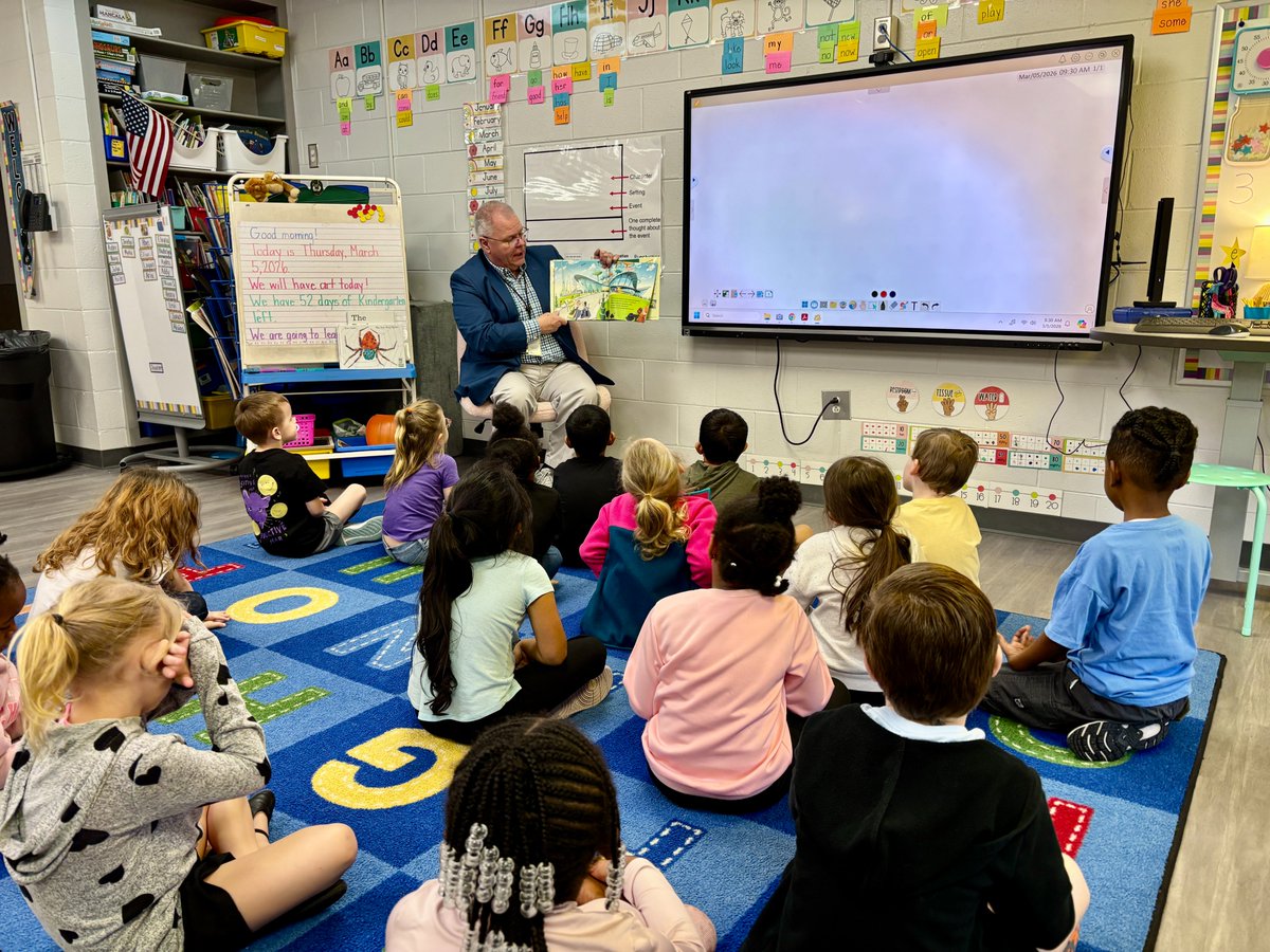
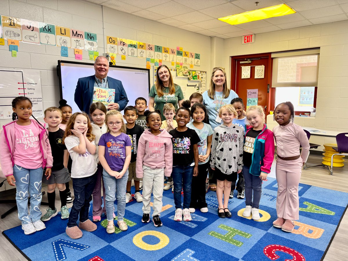
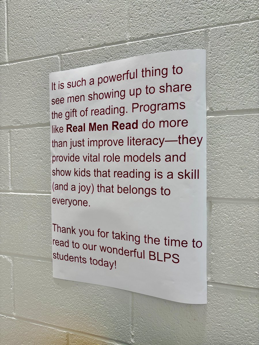
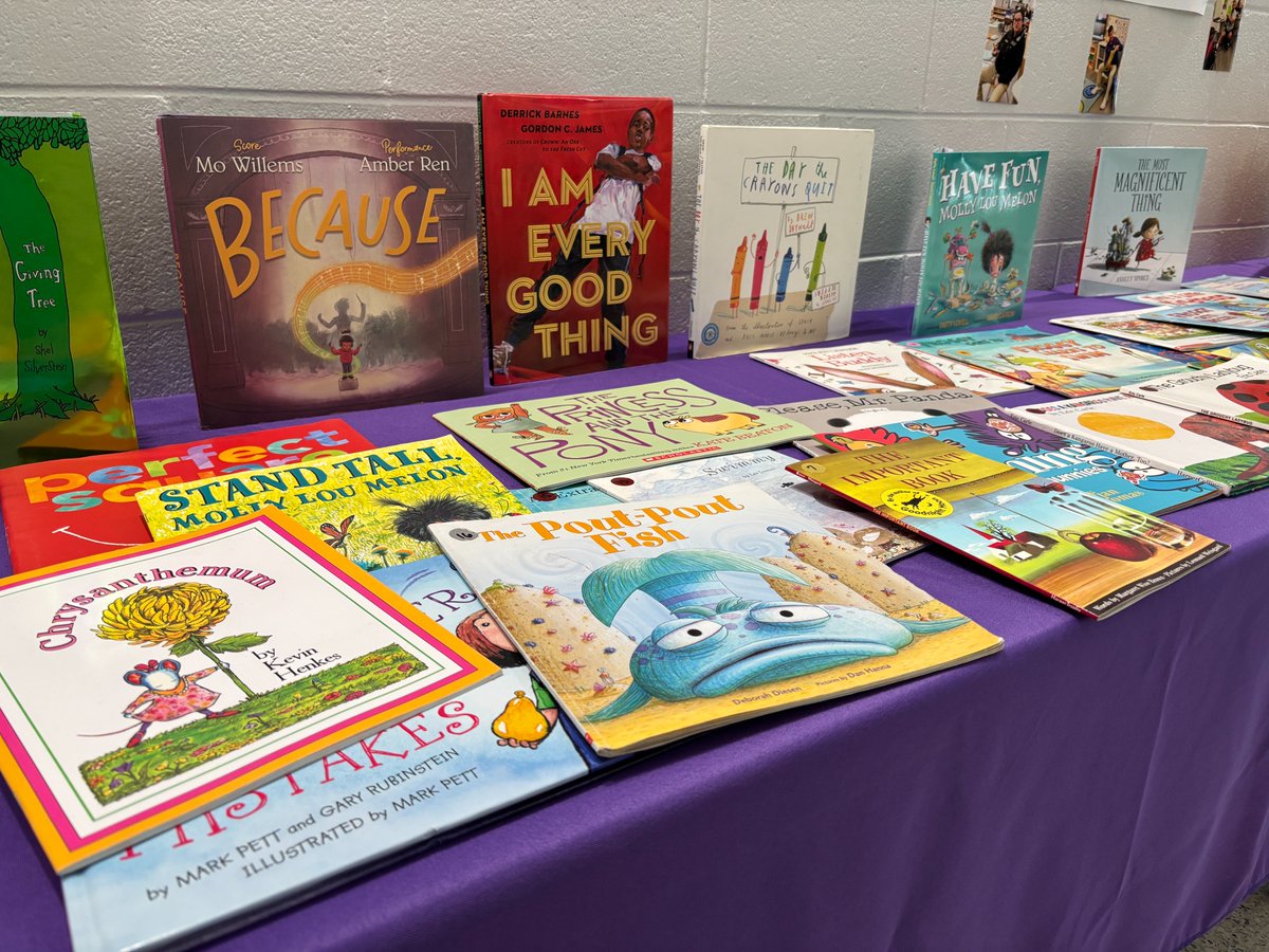
Lex3 Superintendent Dr. Ashley Atkinson spent time at B-L Primary School today sharing the joy of reading with students as part of our Read Across America Week celebrations! Dr. Atkinson joined classrooms to read & highlight the importance of building a lifelong love of books.
2
59


30 Jul 2025
🐾We’re better together Panther families! 🐾
Tomorrow (Thursday, July 31st) is the big day — our annual Meet the Teacher event — and our Lex3 staff members are already smiling because they get to see YOU soon!
Get all of the event details here: lex3.org/page/meet-the-teach…
1
2
100
29 May 2025
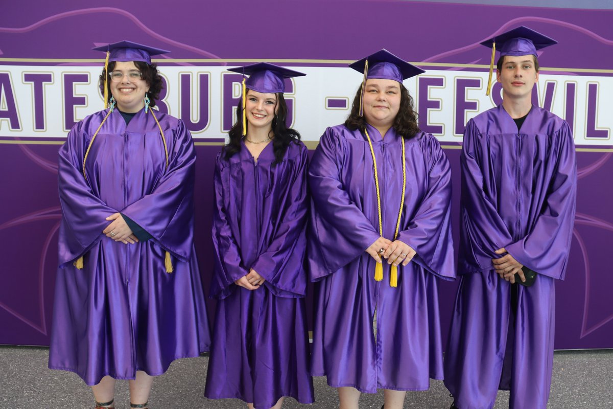
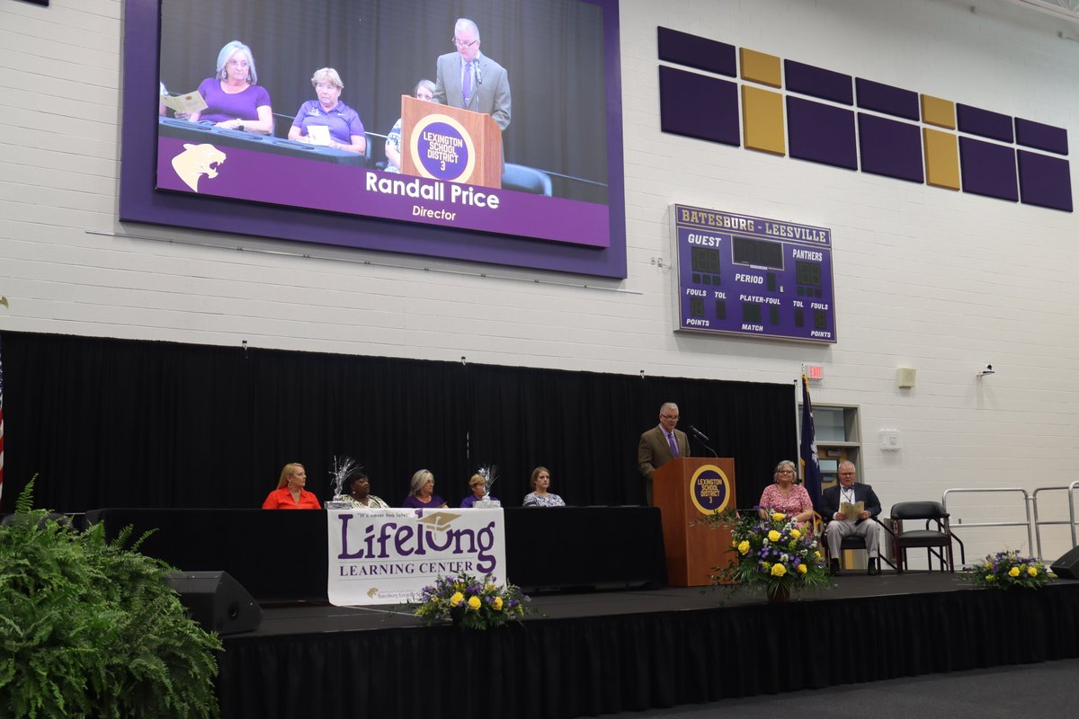
On Wednesday, May 28th, Lexington Three’s Lifelong Learning Center hosted a Graduation Ceremony for the Adult Education Class of 2025 in the B-L High School gym. As you turn the page to your next chapter, know that your #lex3 family is cheering you on every step of the way!
3
121

25 May 2025
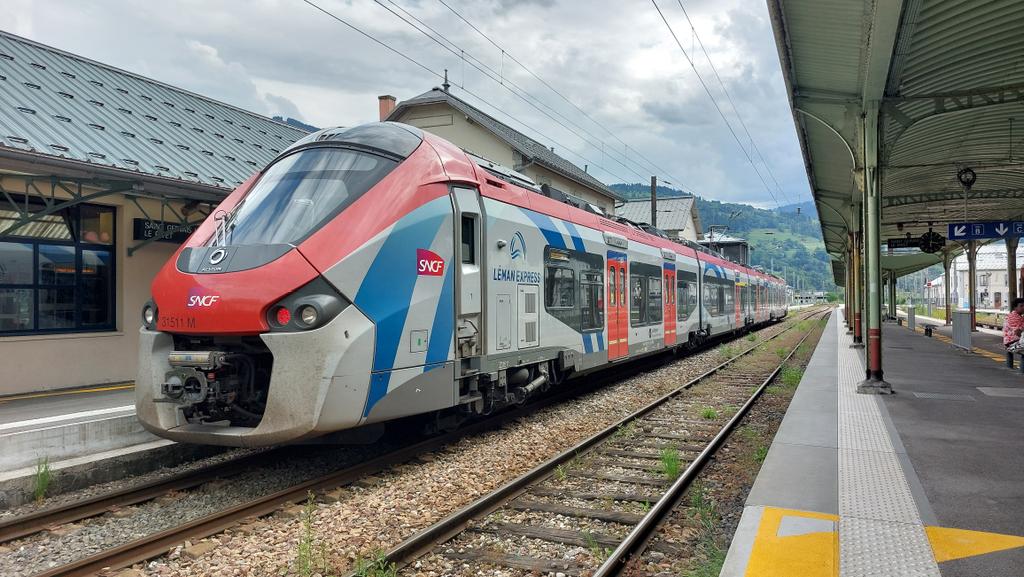
Le Train LEX3 [Course #23466, en provenance de Coppet a été reçu sur la voie A de Saint-Gervais les Bains le Fayet

11
277
23 Apr 2025
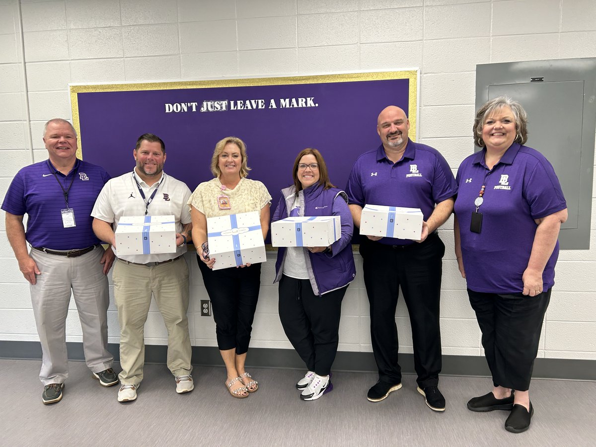
Today we celebrate the heart of every school and office—our incredible administrative professionals! Their hard work, attention to detail, and constant support keep everything running smoothly here in Lex3 day in and day out.
2
72

📅 Zapisz datę! LEX3 – Śląsk, 12–13.06.2025 🇵🇱 Innowacje, technologie, networking dla MŚP 💶 500€ wsparcia! 👉 info@idealist-project.eu #SMEs #MŚP #Innowacje @aerosilesia #przemysł #lotnictwo

1
2
50
7 Feb 2025
Three of our district's choral teachers are spending the day in Columbia at the SC Music Educators Association conference.
Pictured from left to right are BLMS teacher Megan Reagan, BLHS teacher Cheryl Felder, and BLES teacher Kristen Pugh.
We love the arts in #lex3!

4
117

25 Oct 2024
October is National Principals Month and we couldn’t be prouder to celebrate the incredible leaders we have in Lex3! Join us in honoring:
Mary Anne Tillman – Principal of BLPS
Matt Velasquez – Principal of BLES
Sharah Clark – Principal of BLMS
Will McGinty – Principal of BLHS
1
4
121
17 Oct 2024
Make plans now to support the BLHS Panther Players as they present "Little Shop of Horrors" at the Lex3 Fine Arts Center! **Please be aware that this play is intended for older students and adults and may be frightening for younger children. Parental discretion is recommended.**

1
4
104

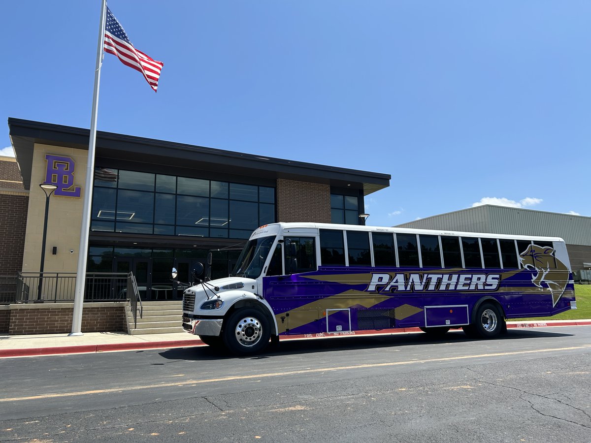
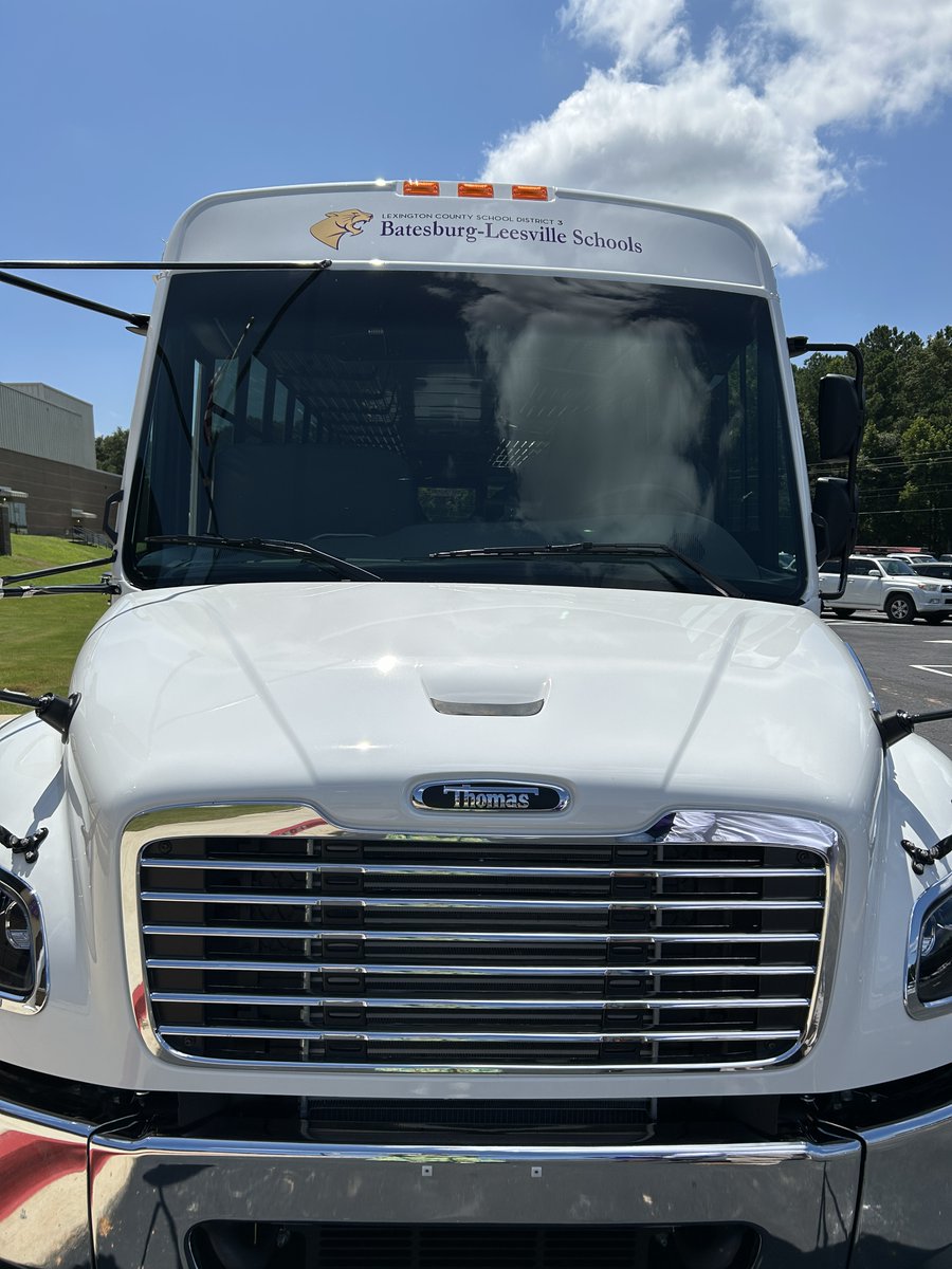
20 Aug 2024
#lex3 just got a new set of wheels! Our latest activity bus is wrapped and ready to roll, bringing Panther pride to every stop it makes. Keep an eye out for our stylish ride—it’s more than transportation, it’s a moving symbol of our amazing district! #lexington3istheplacetobe
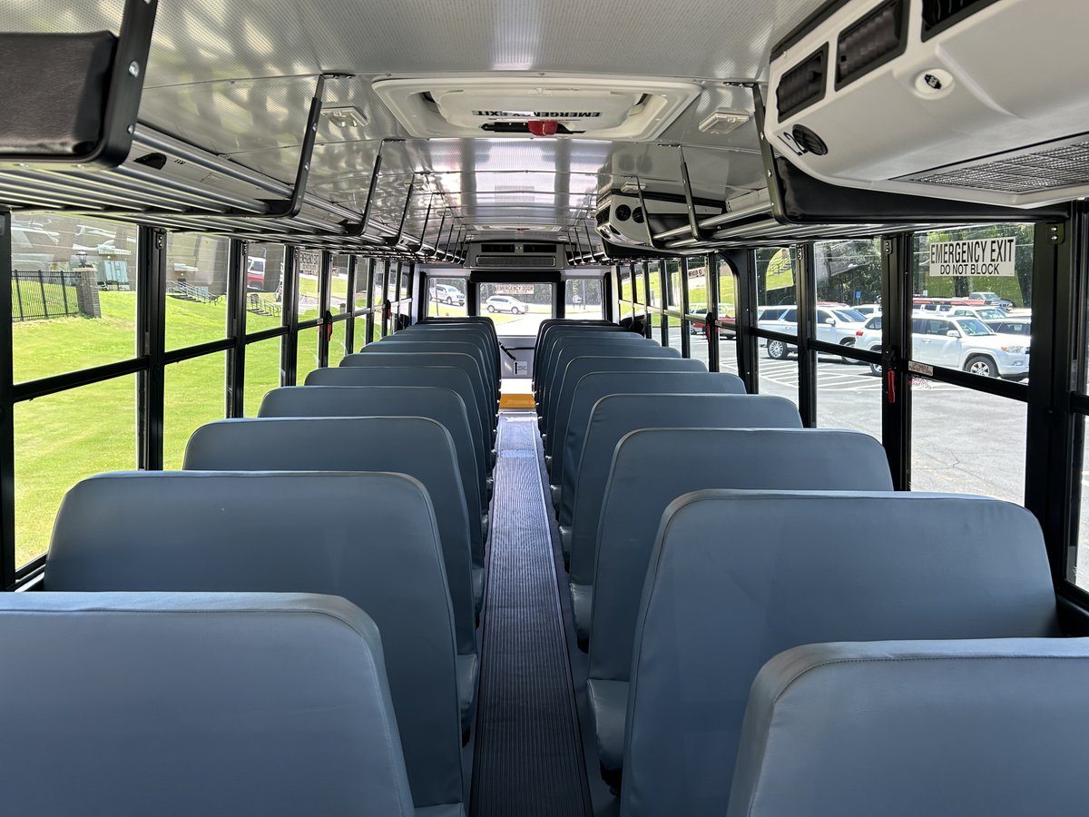
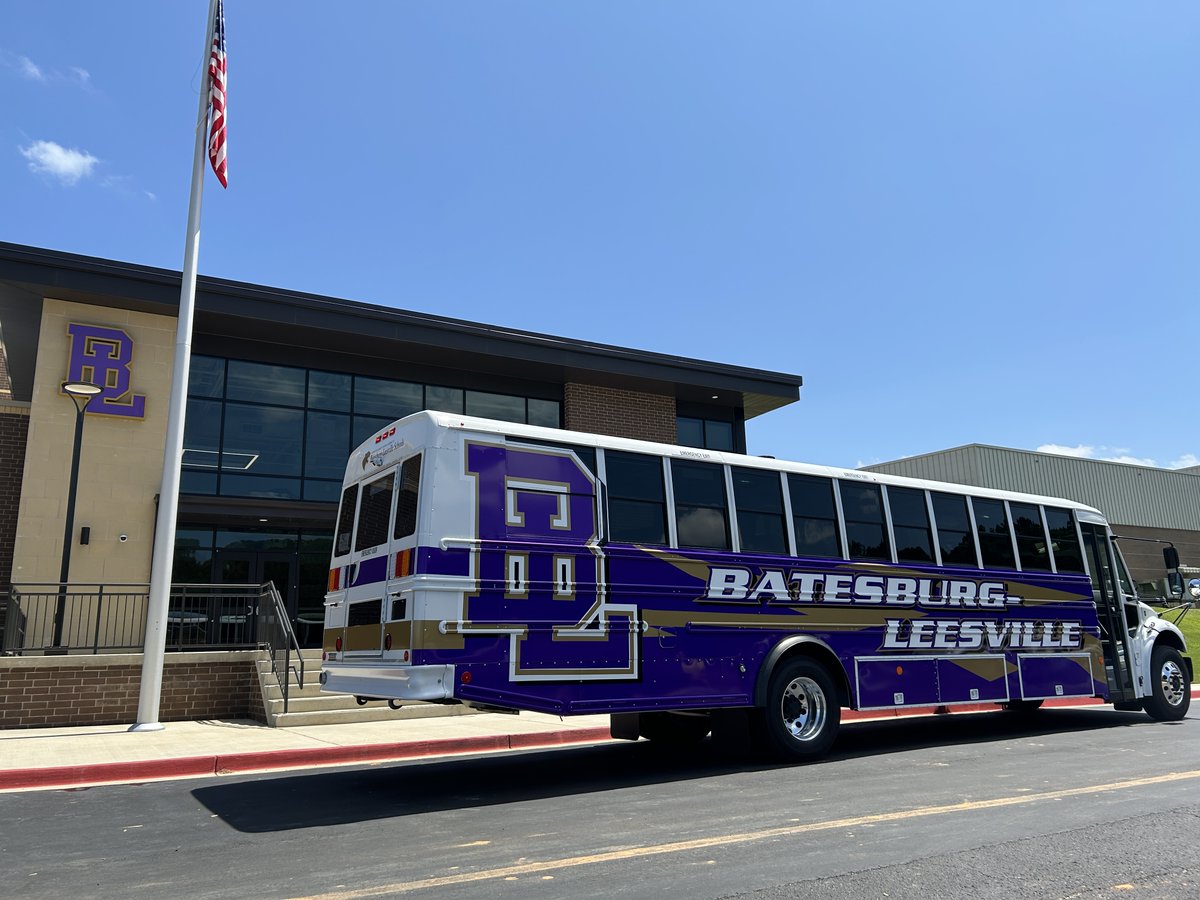
4
98