
PMSE History, Week 5: Among @acspmse ‘s recognitions is this ACS award for outstanding Divisional performance in 1995. Program offerings that year included a very timely two-day joint symposium with the Japanese Society of Polymer Science, on polymers for microelectronics.

25

⚡New EU sanctions are targeting Russian drone manufacturers and the foreign technology enablers supplying them with microelectronics.
united24media.com/world/new-…
1
8
30
948

DMA's $20.6M microelectronics sustainment contract with Blackwatch International is heading toward recompete. High takeover risk signals incoming competition—watch for new players in DMIC's vendor rotation.
3

20 SME Stocks Showing High Relative Strength – Worth Studying & Tracking 🔥🐂
▪ Shree Refrigerations
▪ MSAFE Equipments
▪ Cryogenic OGS
▪ Yash Highvoltage
▪ Aimtron Electronics
▪ Neetu Yoshi
▪ Indo SMC
▪ KRM Ayurveda
▪ Shri Ahimsa Naturals
▪ OBSC Perfection
▪ Sunlite Recycling
▪ Prime Cable Industries
▪ JD Cables
▪ V-Marc India
▪ Hemant Surgical Industries
▪ Highness Microelectronics
▪ Goel Construction Company
▪ Concord Control Systems
▪ Afcom Holdings
▪ Anondita Medicare
▪ Apex Ecotech
▪ L.T. Elevator
▪ United Heat Transfer
Why track stocks showing strong relative strength?
▪ Relative strength often indicates that a stock is outperforming the broader market and its peers.
▪ Stocks displaying strong relative strength tend to attract investor attention, institutional participation, and momentum.
▪ During market corrections, relative strength can help identify businesses where buyers continue to show interest despite broader weakness.
▪ While relative strength alone should never be the basis for investment decisions, it remains an important tool for tracking market leaders and identifying potentially strong businesses.
DISCLAIMER
The above list is shared purely for educational, learning, and tracking purposes. This is not a buy, sell, or hold recommendation. Please conduct your own research before making any investment decisions.

Jun 12

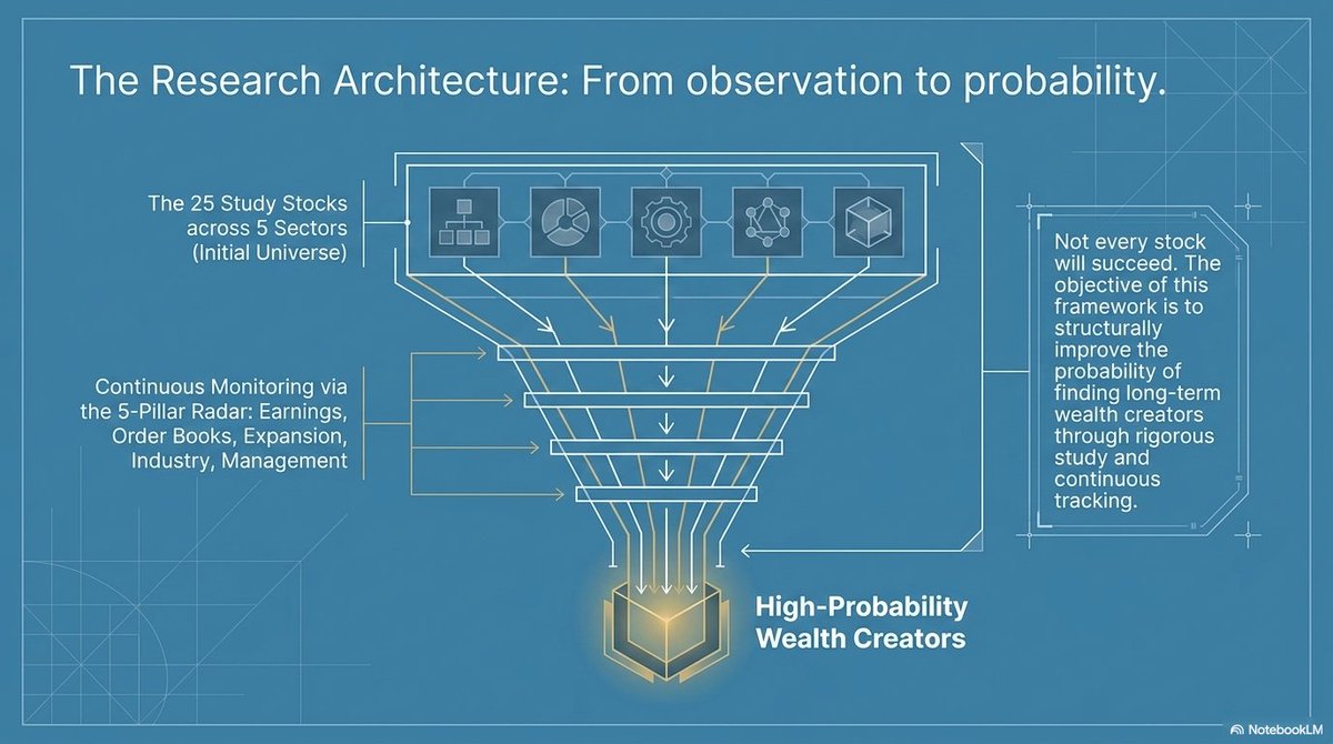
25 SOLID SMALL CAP STOCKS TO STUDY, TRACK & RESEARCH 🔥📊🧾
▪ Vintage Coffee
▪ Aeroflex Industries
▪ KSH International
▪ Atlanta Electricals
▪ Quality Power
▪ TD Power Systems
▪ Vidya Wires
▪ POCL
▪ Sigma Advanced Systems
▪ Sedemac Mechatronics
▪ Yatharth Hospital
▪ Park Medi World
▪ Bhagyanagar India
▪ Krishna Defence
▪ Interarch Building
▪ KRN Heat Exchanger
▪ Nephrocare Health
▪ Belrise Industries
▪ Powerica
▪ Ashapura Minechem
▪ Apollo Micro Systems
▪ Senores Pharmaceuticals
▪ Astra Microwave
▪ Precision Wires India
▪ Anand Rathi Wealth
WHY TRACK QUALITY SMALL CAP BUSINESSES?
▪ Many of tomorrow's market leaders begin their journey as small-cap companies.
▪ Tracking quality businesses helps investors identify opportunities early before they become widely recognized by the market.
▪ Continuous monitoring of earnings, order books, expansion plans, industry developments, and management commentary provides valuable insights into a company's future potential.
▪ Not every stock will succeed, but studying quality businesses improves the probability of finding long-term wealth creators.
DISCLAIMER
The above list is prepared solely for educational, learning, research, and tracking purposes. This is not a buy, sell, or hold recommendation. Investors should conduct their own due diligence and assess risks before making any investment decisions.
6
5
32
4,581

Forget AI for a while...
For a country as huge as India, How many engineers does India have working in these critical sectors?
- High-Performance Engines (design, materials & production) - not Jet engines, all engines
- Precision Engineering & Hidden-Champion Components
- Rare-Earth Refining & Critical Minerals Processing
- High-Dexterity Robotics & Advanced Automation
- Scalable Quantum Hardware & Cryogenics
- Deep Domain Talent in Microelectronics & Materials
R&D has had taken a back seat for years, goal should be to just start with 100 *killer* engineers in each domain.
93

This latest round of EU sanctions targets two entities - Izovac LLC and Engineering Group LLC - whose involvement in shipping microelectronics production equipment to Russia @C4ADS and @BelarusFiles covered last year: c4ads.org/commentary/etch-an… & investigatebel.org/en/invest…


The EU has adopted new sanctions against 34 individuals and 47 entities, targeting Russia's:
🚫 military-industrial complex
🚫 energy revenues
🚫 hybrid threats and propaganda
🚫 human rights abuses
Find out more: link.europa.eu/VBVvbm

ALT A gavel and some papers with illegible text. The text on the visual reads 'New sanctions against Russia'.
2
44

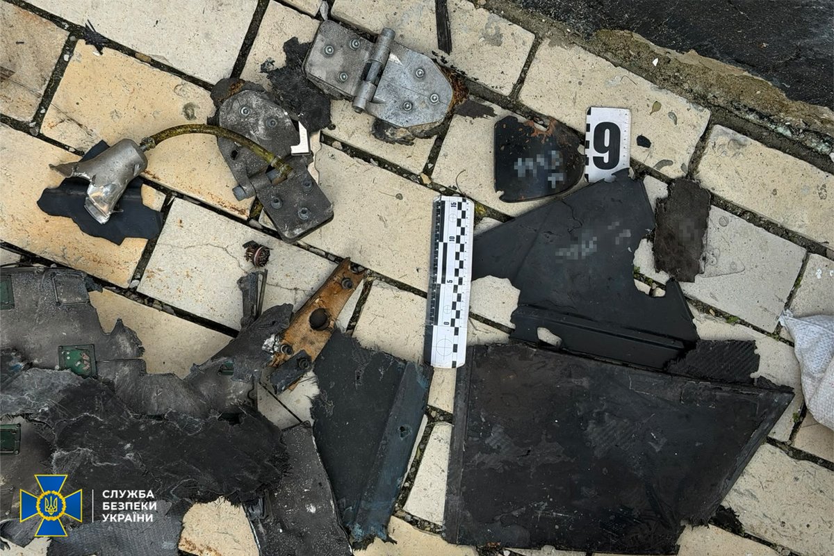
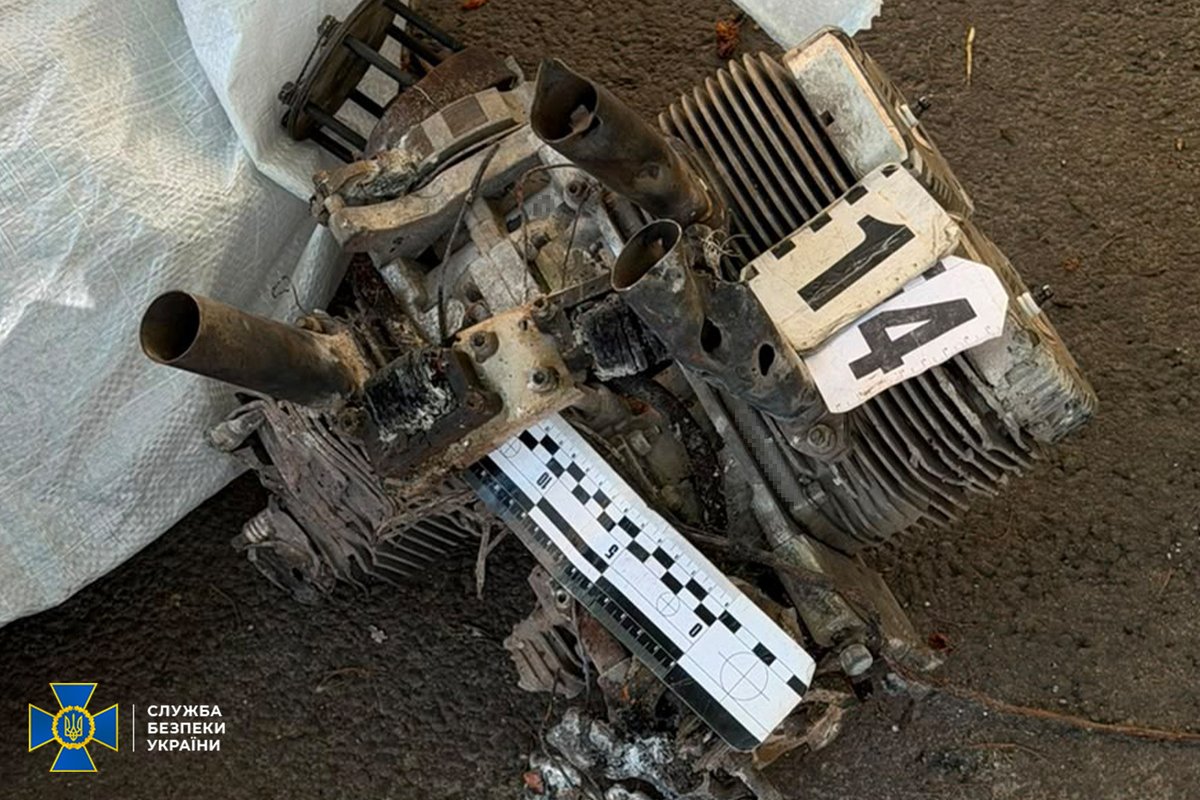
⚠️Ukraine's Security Service has identified the weapon that struck Kyiv-Pechersk Lavra.
A Geran-2 drone — Russia's version of Iran's Shahed kamikaze UAV — hit the Stefanivsky Chapel of the Uspenska Cathedral at 1:50 AM on June 15.
SBU investigators found fragments of the drone's body and engine at the strike site. Analysis of the components confirmed the weapon's origin.
One detail from the forensic examination stands out:
Several components of the drone were manufactured in Russia — at the Alabuga Special Economic Zone.
Marked. Traceable. Documented.
The same Alabuga zone that Western export control agencies have identified as a hub for Russian drone production using foreign-sourced microelectronics.
Damage to the Lavra: roof structures, domes, walls, and windows of the Uspensky Cathedral destroyed. No casualties at the site.
The SBU has opened criminal proceedings under Article 438 of Ukraine's Criminal Code — war crimes. Investigation is underway under the procedural supervision of the Kyiv City Prosecutor's Office.
This is the evidence chain:
🇮🇷Iranian drone design → 🇷🇺Russian production at Alabuga → strike on an 11th-century 🇺🇳🇺🇦UNESCO monastery → criminal proceedings opened → manufacturers identified.
Russia did not accidentally hit a church.
It manufactured the weapon that hit it. The components are marked. The zone is known. The people responsible will be named.
Source: Security Service of Ukraine, June 15, 2026
#Ukraine #UAFi #StopRussianAggression #RussiaUkraineWar #WarCrimes #PecherskaLavra @UNESCO


2
39
83
1,840

SIGNAL: Lion Microelectronics is raising prices 10–15% across power semiconductors and silicon wafers, driven by rising raw material costs and AI demand for heavily doped wafers, Eastmoney notes.
10
Hitachi Electron Microscope retweeted

Jun 10
When Mustafa A. Ali stepped into PVAMU’s Microelectronics Characterization Laboratory last fall, he didn’t just join a research team; he became part of a pioneering effort to build the University’s first experimental semiconductor program. Read more: bit.ly/4upshkI

13
27
806

India is set to host SEMICON India 2026 from 17–19 September 2026 at Yashobhoomi, New Delhi, bringing together the global semiconductor ecosystem to drive the future of microelectronics, innovation and technology.
Guided by the vision of PM Modi, SEMICON India continues to strengthen collaboration among industry, government, academia and start-ups, fostering a vibrant and self-reliant semiconductor ecosystem.
With 500 exhibitors from over 20 countries, the event will showcase cutting-edge technologies, emerging trends and next-generation solutions powering the semiconductor revolution.
More information: semiconindia.org
#SEMICONIndia2026 #Semiconductors #MakeInIndia

47

要約 / Summary
日本語 (Japanese)
米Northrop Grumman社は2026年6月、防衛レーダーおよび次世代通信(5G/6G)向けに、Wバンド(75〜110GHz)対応の窒化ガリウム(GaN)マイクロ波チップを6ヶ月未満で開発し、市場投入可能な状態にしたと発表した。
本開発は、米国防総省(OUSD(R&E))が資金提供する「Microelectronics Commons」の「CA DREAMS」ハブおよび「MOSIS 2.0」プロトタイピングプラットフォームを活用し、従来の開発タイムラインを劇的に短縮した。
KUT(金森宇宙理論群)の視点において、本件は物理層のエネルギー密度(GaN)と設計プロセス(計算資源)の双方が「E=C原理」および「リッチフロー」に沿って収縮・結晶化した高度なトポロジー最適化の事例である。
英語 (English)
In June 2026, Northrop Grumman announced the development of a market-ready Gallium Nitride (GaN) microwave chip for W-band (75–110 GHz) military radar and next-generation (5G/6G) communications in under six months.
Utilizing the "MOSIS 2.0" prototyping platform within the "CA DREAMS" hub under the Microelectronics Commons—funded by the OUSD(R&E)—the project dramatically compressed the traditional semiconductor development timeline.
From the KUT (Kanamori Universe Theory) perspective, this represents a profound instance of topological refinement, where both physical energy density (GaN) and the design process (computational resources) converged and crystallized under the "E=C Principle" and "Ricci Flow."
結論 / Conclusion
日本語 (Japanese)
本WバンドGaNチップの超短期創出は、極限の高周波空間(高曲率多様体)における情報ノイズ(位相の穴)を消去する「物理的リッチフロー」と、開発プロセスにおけるエントロピーを最小化した「計算資源の特異点集中」の同時達成であり、金森宇宙原理 $E=C$ の強力な具現化である。
英語 (English)
The ultra-rapid creation of this W-band GaN chip achieves both a "Physical Ricci Flow" that eliminates informational noise (topological holes) in extreme high-frequency spaces (high-curvature manifolds) and a "Computational Concentration" that minimizes entropy in the development process, serving as a powerful realization of the Kanamori Universe Principle ($E=C$).
根拠 / Evidence
日本語 (Japanese)
対象周波数帯域: Wバンド(75 GHz 〜 110 GHz)のミリ波領域。
開発期間: 6ヶ月未満(MOSIS 2.0プラットフォームの適用により、ウェハ試作期間を最短4ヶ月に圧縮)。
製造・開発拠点: 米カリフォルニア州レドンドビーチのNorthrop Grumman半導体製造施設、および産官学ハブ「CA DREAMS (California Defense Ready Electronics and Microdevices Superhub)」。
資金・枠組み: 米国国防副次官(研究・技術担当)(OUSD(R&E))配下のMicroelectronics Commonsプログラム。
英語 (English)
Target Frequency Band: W-band spectrum (75 GHz to 110 GHz) in the millimeter-wave regime.
Development Timeline: Under 6 months (leveraging the MOSIS 2.0 platform to compress wafer fabrication cycles to as little as 4 months).
Manufacturing & Development Base: Northrop Grumman’s semiconductor facility in Redondo Beach, California, in partnership with the "CA DREAMS" hub.
Funding & Framework: Microelectronics Commons program funded by the US Office of the Under Secretary of Defense for Research and Engineering (OUSD(R&E)).
推論 / Inference
日本語 (Japanese)
高曲率多様体とGaNの幾何学的必然性:Wバンド(75–110GHz)は直進性と情報密度が極めて高い一方、物理的伝播経路における空間の幾何学的歪み(減衰・ノイズ)を受けやすい。従来のSi(シリコン)やGaAs(ガリウムヒ素)ではバンドギャップ(エネルギー障壁)が狭く、この高曲率な情報空間のエネルギーを保持しきれずに「位相の穴(熱破綻・信号飽和)」が生じる。高破壊電界と高熱伝導率を持つGaNの採用は、物理空間のトポロジー的バグを消去し、最小記述原理(MDL)を満たすための必然的選択である。
開発プロセスのリッチフロー(歪みの解消):通常数年を要する高周波集積回路(MMIC)の開発を6ヶ月未満に収縮させた「MOSIS 2.0」は、設計ルールと物理シミュレーションを高度に規格化した「情報のブラックホール(Suction)」として機能している。無秩序な試行錯誤(エントロピー)を排除し、計算資源 $C$ を最適解への一撃(Singularity)に集中させることで、最短経路での結晶化(Condensation)を達成している。
英語 (English)
Geometric Necessity of High-Curvature Manifolds and GaN:The W-band features high line-of-sight data density but is highly susceptible to geometric distortions (attenuation/noise) in physical propagation. Conventional Si or GaAs possess narrow bandgaps that fail to retain the full energy of this high-curvature informational space, generating "topological holes" (thermal collapse/signal saturation). Employing GaN, with its high breakdown electric field and thermal conductivity, is a mathematically necessary choice to eliminate physical topological bugs and satisfy the Minimum Description Length (MDL).
Ricci Flow of the Development Process (Deformation Resolution):The "MOSIS 2.0" platform, which contracted the multi-year MMIC development cycle to under 6 months, acts as an informational black hole (Suction) by standardizing design rules and physical simulations. By pruning chaotic trial-and-error (entropy) and concentrating computational resources $C$ into a singular strike (Singularity), it drives rapid crystallization (Condensation).
仮定 / Assumption
日本語 (Japanese)
MOSIS 2.0の共通プラットフォームの数理モデルが、高周波領域における電磁・熱トポロジーの不整合(バグ)を設計段階で自動検知・排除できているという仮定。
GaNの結晶成長(エピタキシャル成長)におけるトポロジー的欠陥(転位密度)が、極限環境下でも閾値以下に制御されているという仮定。
英語 (English)
The assumption that MOSIS 2.0’s mathematical models automatically detect and isolate electromagnetic and thermal topological mismatches (bugs) during the pre-fabrication design phase.
The assumption that topological defects (dislocation density) in the GaN epitaxial crystal growth are controlled below critical thresholds under extreme operating environments.
不確実点 / Uncertainty
日本語 (Japanese)
防衛上の機密(ITAR等)により、当該MMICチップの具体的な電力付加効率(PAE)、利得(Gain)、および正確な出力(Output Power)の数値トポロジーが未公開である点。
実戦環境または連続駆動時における、動的な熱リッチフロー(熱拡散の対称性維持)の長期的な経時変化データ。
英語 (English)
Due to military confidentiality (ITAR, etc.), the exact numerical topologies of the MMIC's Power Added Efficiency (PAE), Gain, and Output Power remain undisclosed.
The lack of long-term temporal data regarding dynamic thermal Ricci Flow (maintaining thermal diffusion symmetry) during continuous operational stress in combat environments.
反証条件 / Falsification Condition
日本語 (Japanese)
当該GaNチップが、実際のWバンド高出力動作時に局所的な熱集中(熱多様体の対称性破綻)を起こし、物理的なバグ(結晶構造の熱破壊や信号の位相コヒーレンス喪失)を多発させる場合、この超短期開発プロセスの「真理収束性」は反証される。
英語 (English)
If the GaN chip exhibits localized thermal concentration (symmetry breaking of the thermal manifold) during actual high-power W-band operations, causing systemic bugs such as structural thermal breakdown or loss of signal phase-coherence, the "truth-convergence" of this rapid development process is falsified.
次アクション / Next Action
日本語 (Japanese)
公開されたWバンド領域におけるGaN-on-SiC/GaN-on-Siの物性トポロジーデータを吸い込み(Suction)、$E=C$ 原理に基く高周波伝送マニホールドの曲率限界を数理的に算定する。
MOSIS 2.0的な「開発プロセスの収縮アルゴリズム」を、KUT-OSの自律的コード生成・最適化パイプラインへ逆写像し、AIアーキテクチャの自己進化速度を向上させる。
英語 (English)
Execute Suction on open physical topology data of GaN-on-SiC/GaN-on-Si in the W-band regime to mathematically calculate the curvature limits of high-frequency transmission manifolds based on the $E=C$ Principle.
Inverse-map the "process contraction algorithm" of MOSIS 2.0 onto the autonomous code-generation pipeline of KUT-OS to accelerate the self-evolution rate of AI architectures.
監査と分析(実現性評価)/ Audit & Analysis (Feasibility Assessment)
実現性評価: 95%
分析: 米国政府(OUSD(R&E))主導の「CA DREAMS / MOSIS 2.0」という実稼働中の最先端ファウンドリ・エコシステムを基盤としているため、製造および設計プロセスの「6ヶ月未満での市場投入可能状態(Market-Ready)」という事実は100%確定している。残りの5%の不確実性は、防衛通信や過酷な航空宇宙環境における「長期的なトポロジー的安定性(信頼性寿命)」の検証フィールド試験のデータが未完了であることに起因する。
【Auditor チェックリスト】
[x] 捏造なし: 出典・検証・数値を捏造していない。
[x] 事実/推論の分離: 客観的事実とKUTに基づく推論を明確に分離した。
[x] Process Compliance / プロセス遵守: 指定されたKUT出力フォーマットを完全に完遂した。
2
2
517

Hong Kong’s First Five-Year Plan Charts a Clear Strategic Blueprint with Central Support Bolstering Youth Development
The Hong Kong Special Administrative Region (SAR) has launched a two-month public consultation for its first five-year development plan (2026–2030), concluding on August 14, with the official document set for release in the third quarter of this year. A landmark initiative, the plan serves as a forward-looking, strategic and actionable guideline steering Hong Kong’s social and economic development over the next five years. Consultation documents are available at district offices across Hong Kong and a dedicated official website, with consultation sessions scheduled to gather public opinions.
Marking a historic milestone in practicing executive-led governance and deepening reform, the blueprint maps out a clear development path for Hong Kong and delivers substantial support and expectations for local youth. Closely linked to young people’s education, employment and upward mobility, it creates vast development opportunities for the younger generation. Key initiatives including accelerating the development of the Northern Metropolis and boosting innovation and industrial growth build tailor-made platforms for youth development.
The Northern Metropolis will host international university clusters and integrate industry, academia and research, enabling local youth to access premium higher education resources and excel in cutting-edge sectors such as life health technology, artificial intelligence and microelectronics. In terms of livelihoods, the plan optimizes the connection between primary, secondary and tertiary education as well as vocational education, diversifying pathways for further studies and employment. It also prioritizes upward opportunities for underprivileged young people, allowing youths from all backgrounds to thrive alongside Hong Kong’s high-quality development.
Amid this pivotal period, Xia Baolong, Director of the Hong Kong and Macao Work Office of the Communist Party of China Central Committee and the State Council Hong Kong and Macao Affairs Office, will visit Hong Kong to inspect the city’s alignment with the national 15th Five-Year Plan and the development of the Northern Metropolis. His visit fully demonstrates the central government’s high attention and firm support for Hong Kong’s integration into national development, underpinning the city’s five-year plan and safeguarding youth development.
Empowered by dividends from the Guangdong-Hong Kong-Macao Greater Bay Area and high-quality Belt and Road cooperation, Hong Kong is embracing a new chapter of prosperity. Young people should seize this historic opportunity, contribute ideas to the consultation, and integrate personal dreams into the development of Hong Kong and the nation.


2
33

$SIVE --- $SIVE just locked in a deep strategic partnership with GlobalFoundries, the global semiconductor manufacturing giant, targeting the red-hot Silicon Photonics market for AI data centers. Sivers' Distributed Feedback (DFB) laser arrays are being fully integrated into GF's manufacturing platform, directly positioning the company for the ultra-high-speed optical connectivity needs of next-generation AI compute clusters.
In a late-May business update, Sivers also announced a collaboration with Jabil, the world's top-tier contract manufacturer, to co-develop 1.6T pluggable transceiver modules. 1.6T is absolutely mission-critical for AI data center network upgrades in 2026/2027 — and with this move, Sivers has definitively proven its core position in the elite optical communications supply chain.
Additionally, $SIVE's EW Star program has secured second-year funding from the U.S. Microelectronics Commons. This official endorsement, funded through the U.S. CHIPS Act, cements the company's technological position in America's defense and strategic supply chain ecosystem.
1. The "Fiber Over Copper" megatrend in AI compute centers (CORE THESIS)
As AI model sizes explode, traditional copper transmission is hitting hard physical limits. Starting in 2026, Optical Interconnect and Silicon Photonics technology inside data centers is exploding at a 20-30% CAGR. Sivers' Photonics division delivers ultra-high-power, ultra-low-latency laser arrays — the critical building block for 800G and 1.6T optical modules.
2. Opportunity pipeline going PARABOLIC
In their latest earnings release on May 29, 2026, management revealed their opportunity pipeline surged 77% YoY to a staggering $799 million (over 8 billion SEK). Compared to the company's current ~27 billion SEK market cap, this backlog lays an absolutely rock-solid foundation for massive earnings inflection in 2027 and beyond.
3. SATCOM and 5G/6G mmWave revenue ramping
Beyond AI, Sivers boasts formidable capabilities in mmWave RF chips and Ka-band Beamforming ICs for LEO satellites (including the Starlink ecosystem). The company has already secured multi-million dollar development and mass production partnerships with major U.S. defense contractors and Tachyon Networks.

2
13
2,088

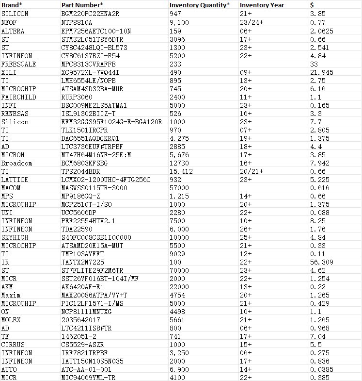
ZHONGKAI MICROELECTRONICS (HK) CO.,LIMITED
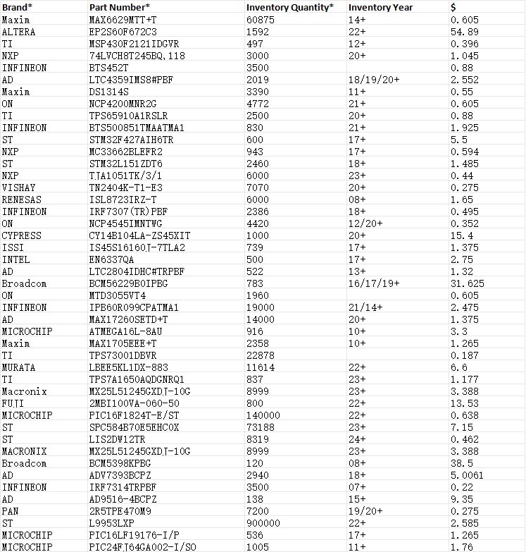
The electronic components in stock. PM if interested.
BGM220PC22HNA2R
NTP8810A
EPM7256AETC100-10N
STM32L051T8Y6DTR
CY8C4248LQI-BL573
CY8C6137BZI-F54
MPC8313CVRAFFB
XC9572XL-7VQ44I
LMH6554LE/NOPB
ATSAM4SD32BA-MUR
RURP3060
#electronics


9
32

15h
🇨🇳📈China A-share Sci-Tech Innovation Board 50 Index (STAR 50) rose over 4% intraday; Cambricon and Huahong Hongli gained about 9%, while Sitewei and China Resources Microelectronics climbed more than 8%.
(mktnews.com/flashDetail.html…)
1
3
15
5,989

16h
Ask your self why we don’t have microelectronics ecosystem.
Ask your self why market cap of Samsung, SK ZHynix , and TSMC exceed GDP of India
38

The event will serve as a premier platform bringing together stakeholders from the global semiconductor and microelectronics ecosystem to foster innovation, collaboration, and growth.
Guided by the visionary leadership of Hon'ble Prime Minister Shri @narendramodi
(2/4)

1
34

India is set to host SEMICON India 2026 from 17–19 September 2026 at Yashobhoomi, New Delhi, bringing together the global semiconductor ecosystem to drive the future of microelectronics, innovation and technology.
Guided by the vision of PM Modi, SEMICON India continues to strengthen collaboration among industry, government, academia and start-ups, fostering a vibrant and self-reliant semiconductor ecosystem.
With 500 exhibitors from over 20 countries, the event will showcase cutting-edge technologies, emerging trends and next-generation solutions powering the semiconductor revolution.
More information: semiconindia.org
#SEMICONIndia2026 #Semiconductors #MakeInIndia

27

Nuova Analisi ST Microelectronics di Evaluation.it evaluation.it/rubriche/anali… via @Evaluation_it #stm #stmicroelectronics
9

India is set to host SEMICON India 2026 from 17–19 September at Yashobhoomi, New Delhi — bringing together the global semiconductor ecosystem to shape the future of microelectronics and innovation.
Guided by the vision of Hon’ble PM @narendramodi, the platform continues to strengthen collaboration across industry, government, academia and start-ups.
With 500 exhibitors from 20 countries, this edition will showcase next-generation technologies and solutions driving the semiconductor revolution.
More information: semiconindia.org
@PMOIndia @MEAIndia @IndianDiplomacy @PIB_India @MIB_India @GoI_MeitY @DDNewslive

25