
Kids proper thick as fuck hence I didn’t reply, he’s thicker than a whale omelette 🤦🏼♂️🤣🤣🤣🤡
2
TheMaskedBandick retweeted

The thicker the berry, the sweeter the juice is what they say 😎
@strawbsmilk420
46
8,886
26,027
1,070,914

Nothing. He aged and he probably had a longer and thicker hair compared to last year. You guys just a bunch of waste of losers.
JOTECH🚘CAR TRACKER🇳🇬 retweeted

Blood is no longer thicker than water!!!
A brother locked up his own blood sister in the house for 2 years without giving her food or water because they had a disagreement over s business they were running together😭😭😭
2
313
🤍I’m Sanwo_Fatimah retweeted

Blood is no longer thicker than water. Nowadays strangers help us more than our relatives. Relatives only accept you when you're successful.
1
2
2
12
Remy Martell Connoisseur retweeted

Jun 15
Thicker than frozen youghurts🥹😍
370
1,136
31,027
681,484
52♿️ retweeted

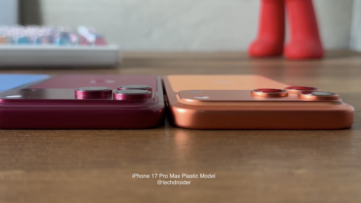
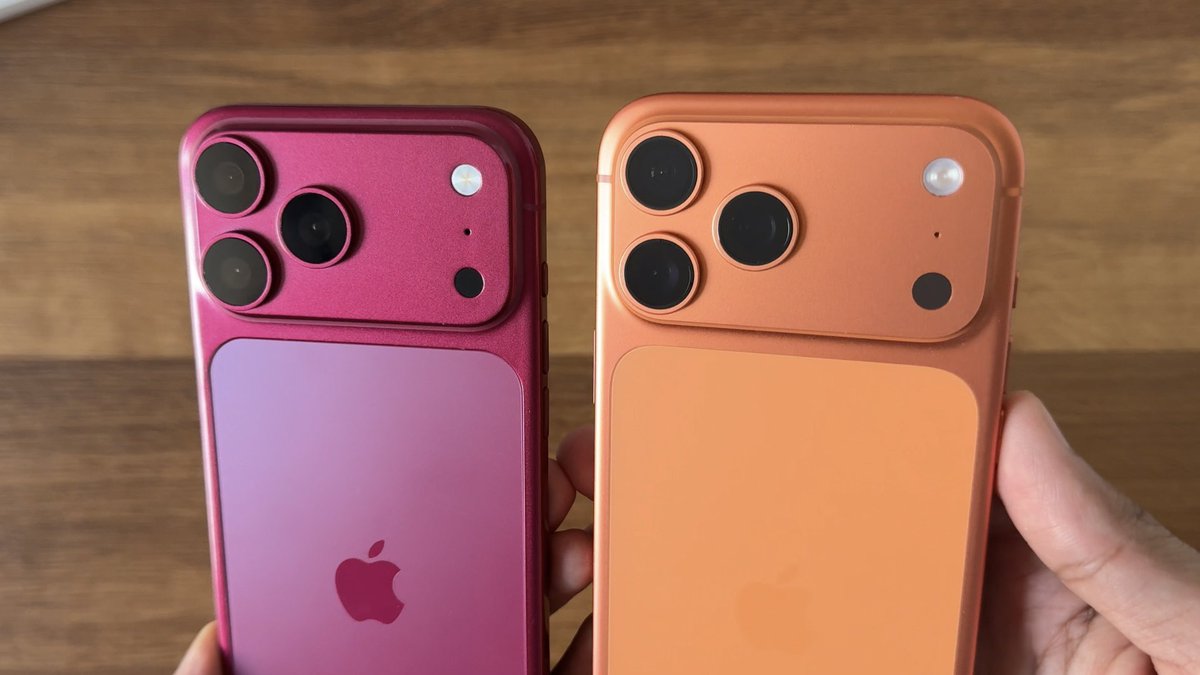
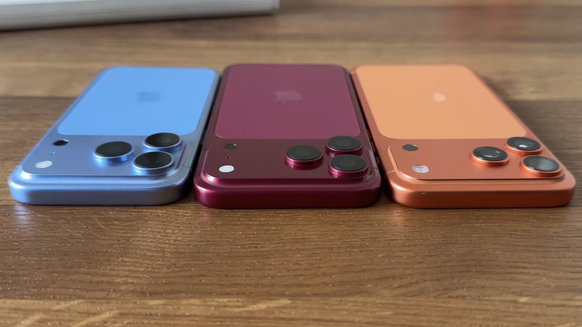
iPhone 18 Pro Max vs iPhone 17 Pro Max - The Camera Bump Just Got Thicker

18
120
2,320
262,376
SneaksFFeet1975 retweeted

Apr 4
Do you like it thicker or longer?
Why not both? 😈🍆

225
1,582
11,785
259,329

The people building smartphones were not letting their own children use them.
Steve Jobs banned iPads at home. His kids had never used one when he died. Bill Gates capped his children's screen time at 30 minutes a day and did not give them phones until they were 14. The senior engineers at Google were sending their kids to Waldorf schools that banned screens entirely.
The people who knew the most about what these products were doing to the developing brain were the ones protecting their own families from them. Almost nobody on the outside was asking why.
A German neuroscientist named Manfred Spitzer was asking why.
In 2012, he published a book called Digitale Demenz, which translates as Digital Dementia. It became one of the bestselling popular science books in German history. The press immediately tried to destroy him. He was called Germany's most controversial brain scientist, a Luddite, a fearmonger, a moral panic merchant.
None of it engaged with the actual neuroscience he was citing.
His thesis was brutally simple. The brain behaves like a muscle. It grows when you use it and atrophies when you don't. Every cognitive task you outsource to a device is a task your brain no longer practices. The neural circuits responsible for that task stop being reinforced. Over time they weaken in exactly the same way an unused muscle weakens.
He was not arguing that smartphones would give you Alzheimer's. He was arguing that decades of cognitive outsourcing would produce measurable decline in the underlying machinery, long before any clinical diagnosis would catch it, and that the decline was already showing up in young adults.
The mechanism is what made him impossible to dismiss.
London taxi drivers who had memorized the entire street map of the city had measurably larger hippocampi than the average person. That is the brain region responsible for spatial memory. Musicians who practiced for thousands of hours had thicker auditory cortices. The brain physically remodels itself in response to use.
Spitzer's argument was just the dark side of the same finding. If it grows in response to use, it must shrink in response to neglect.
The supporting data started landing.
A 2020 study at McGill University tracked 50 regular drivers and measured GPS use. Heavy users had weaker spatial memory, and when researchers retested a subset three years later, those users had declined the fastest. The same hippocampus London cabbies had built by ignoring shortcuts was being slowly hollowed out in everyone else by accepting them.
A 2024 MIT study scanned the brains of people writing essays with and without ChatGPT. The AI group showed 55 percent weaker brain connectivity than the group writing alone. 83 percent of the ChatGPT users could not recall a single line from essays they had written minutes earlier. The damage stayed even when the tool was taken away.
Every one of these findings is exactly what Spitzer predicted in 2012.
The generation he was warning about is now in their twenties. The first cognitive scans of what we did to them are starting to come back. The pattern is what he said it would be.
The people who built the devices already knew. They knew before he published a word.
They just didn't tell anyone outside the family.
The brain you were born with is not the brain you will die with. You are training it every day, with every task you keep and every task you hand off.
The only question is which direction.

1
2
46
monika retweeted

May 31
Puma said ‘Forever Faster’… Kareena heard ‘Forever Thicker’ 😮💨


65
194
4,231
755,422

13m
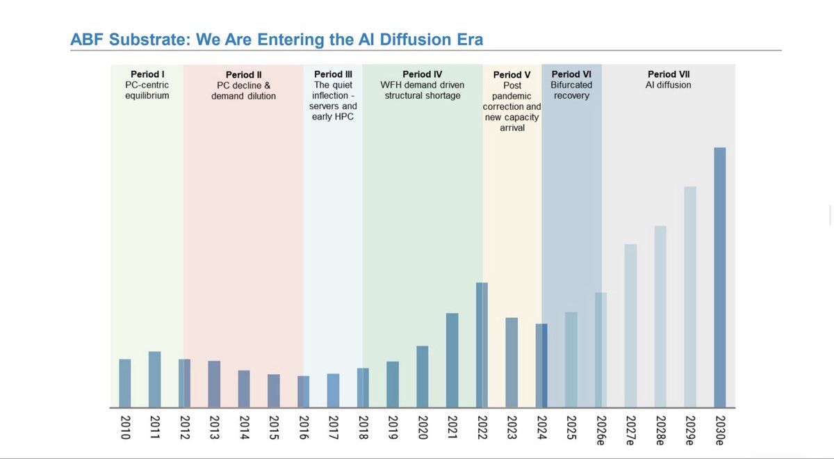
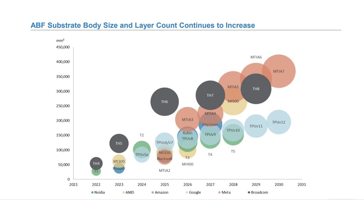
ABF substrate is becoming one of the quiet winners in the AI hardware cycle.
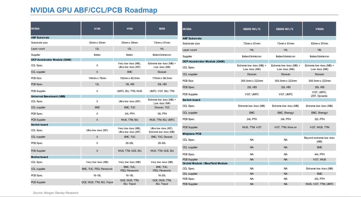
Morgan Stanley’s latest report shows a clear trend: as AI systems move from A100/H100 to B200, GB200/GB300 and VR200, the package substrate is getting larger, thicker and harder to manufacture.
The numbers are straightforward:
A100: 55mm × 55mm, 12 layers
H100: 55mm × 58mm, 12 layers
B200: 73mm × 81mm, 14 layers
VR200: 83mm × 97mm, 18 layers
This is not just a unit growth story. It is a content-per-chip story.
Larger die packages, higher power density, more HBM, and more complex high-speed interconnect all require better substrates, more layers, tighter routing, and higher-end materials.
The same trend shows up at the system level.
For VR200, Morgan Stanley shows OAM module PCB moving to 26-layer HDI, switch board moving to 32-layer PTH, and new demand from midplane PCB and BlueField-related modules.
In other words, AI server architecture is pushing complexity deeper into the hardware stack: ABF substrate, CCL, PCB, power delivery, signal integrity, and thermal design.
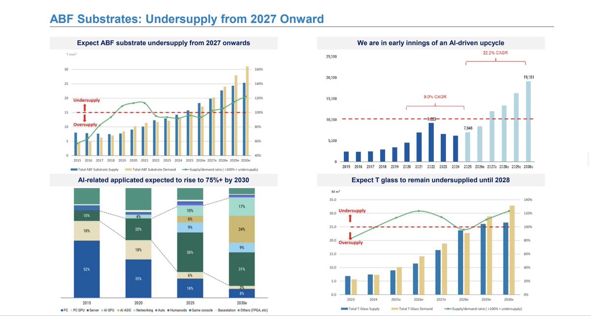
Morgan Stanley also expects ABF substrate to move into undersupply from 2027 onward, with AI-related applications rising to 75% of ABF demand by 2030.
That matters because this cycle is about how much more value each new generation of AI hardware pulls into the supply chain.
ABF is a good example of that.
It sits under the chip, but its importance is moving up.
6

I believe that as we go through life, our relationships with family and friends are like cords that we weave. As we overcome more challenges and difficulties together, the thicker and more strengthened these cords become.


No radical changes shown: It correctly avoids depicting under-display Face ID (not fully ready) or major camera rearrangements, but specifics like exact lens sizes or a potentially thicker Pro Max chassis (~8.8mm) aren't fully detailed in such renders.
1
2
It won't disappear entirely or switch to a simple hole-punch yet.
Camera bump: The renders show a substantial raised module, which matches dummy unit leaks indicating a slightly thicker camera plateau (e.g., ~0.3mm thicker overall, with more protruding lenses) to accommodate upgrades like variable aperture or larger sensors.
1
5

Vinegar, water, oil, sugar, eggs, mustard powder.
Like a tangy, creamy, thicker than a vinegarrete type of dressing/sauce
3
