
418 Photos and videos


Jun 16
I will be adding more $XFAB more if it stays below $10 - NFA though
Jun 16

$XFAB Major achievements so far:
• Technology transfer and process industrialization at X-FAB advancing well.
• Key equipment installed and commissioned (e.g., SiN LPCVD furnace in March 2024; 193 nm lithography tool in early 2025).
• IMEC–X-FAB licensing agreement finalized for the SOI platform.
• Demonstrator Run 1 completed for SOI (including micro-transfer printing of active components); initial optical results on passive waveguides were promising (October 2025).
• InP active chiplets (lasers, modulators, detectors) prepared by SMART Photonics.
• Packaging and assembly design kits deployed (Luceda PHIX).
• Multi-Project Wafer (MPW) activities started with external partners in September 2025.
• Customer Engagement Portal (photonixfab.eu) launched in March 2024 — open for first prototyping, R&D, and low-volume access while industrial processes ramp up.
Next steps (planned for remaining months):
• Design work for final Demonstrator Run 2 starts November 2025.
• PIC fabrication expected early 2026.
• Testing/validation of initial demonstrators targeted by end of 2025.
• Continued refinement of processes toward pilot-line readiness.
58
Jun 16
Quietly $SIVE has now became my 3% of portfolio.
Bullish drivers: AI demand, big pipeline, potential Nasdaq listing (could bring more institutional money).
Risks: High valuation, ongoing losses, potential dilution (up to 15%), short interest, and regulatory scrutiny.
1
67
Jun 16
$XFAB Major achievements so far:
• Technology transfer and process industrialization at X-FAB advancing well.
• Key equipment installed and commissioned (e.g., SiN LPCVD furnace in March 2024; 193 nm lithography tool in early 2025).
• IMEC–X-FAB licensing agreement finalized for the SOI platform.
• Demonstrator Run 1 completed for SOI (including micro-transfer printing of active components); initial optical results on passive waveguides were promising (October 2025).
• InP active chiplets (lasers, modulators, detectors) prepared by SMART Photonics.
• Packaging and assembly design kits deployed (Luceda PHIX).
• Multi-Project Wafer (MPW) activities started with external partners in September 2025.
• Customer Engagement Portal (photonixfab.eu) launched in March 2024 — open for first prototyping, R&D, and low-volume access while industrial processes ramp up.
Next steps (planned for remaining months):
• Design work for final Demonstrator Run 2 starts November 2025.
• PIC fabrication expected early 2026.
• Testing/validation of initial demonstrators targeted by end of 2025.
• Continued refinement of processes toward pilot-line readiness.
95
Jun 16
81
Alpha Hunter retweeted

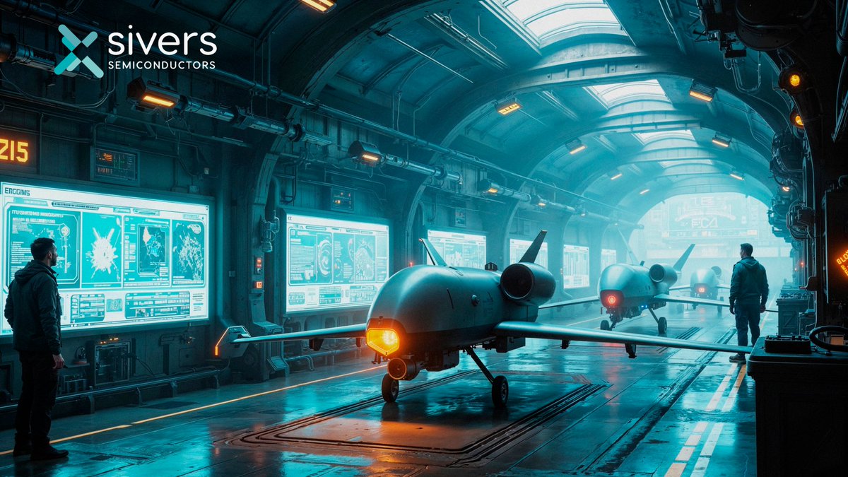
Defense systems require reliable #communication and sensing in complex conditions. Performance must hold across long distances, changing environments, and real-time scenarios.
#Photonics and high-frequency #wireless support these requirements through high-speed data transfer and secure #connectivity. 🛰️
Sivers develops solutions for these types of applications, with advanced #mmWave technology for mission-critical operations. Learn more about Sivers' #defense solutions: sivers-semiconductors.com/ap…
8
35
280
14,332
Jun 15
So war is over, are we adding aggressively?
If so what’s your highest conviction play?
40
Jun 14
CONGRATS MATE!!! 🎉🎉
That’s absolutely HUGE! 🙌🔥
Brunson, you legend! We actually did it! 🍻🏆
Hope you haven’t forgotten your promise… 😆🤣
Can’t wait to collect! 😉🎊
Jun 14

OMG I CAN FEEL IT….
90
Jun 12
SpaceX IPO launched, I failed.
Unsubscribed from Premium - algo not showing posts/replies.
Feels ghost banned.
If you followed me because you liked my posts and want to see my updates, turn on notifications - only way left.
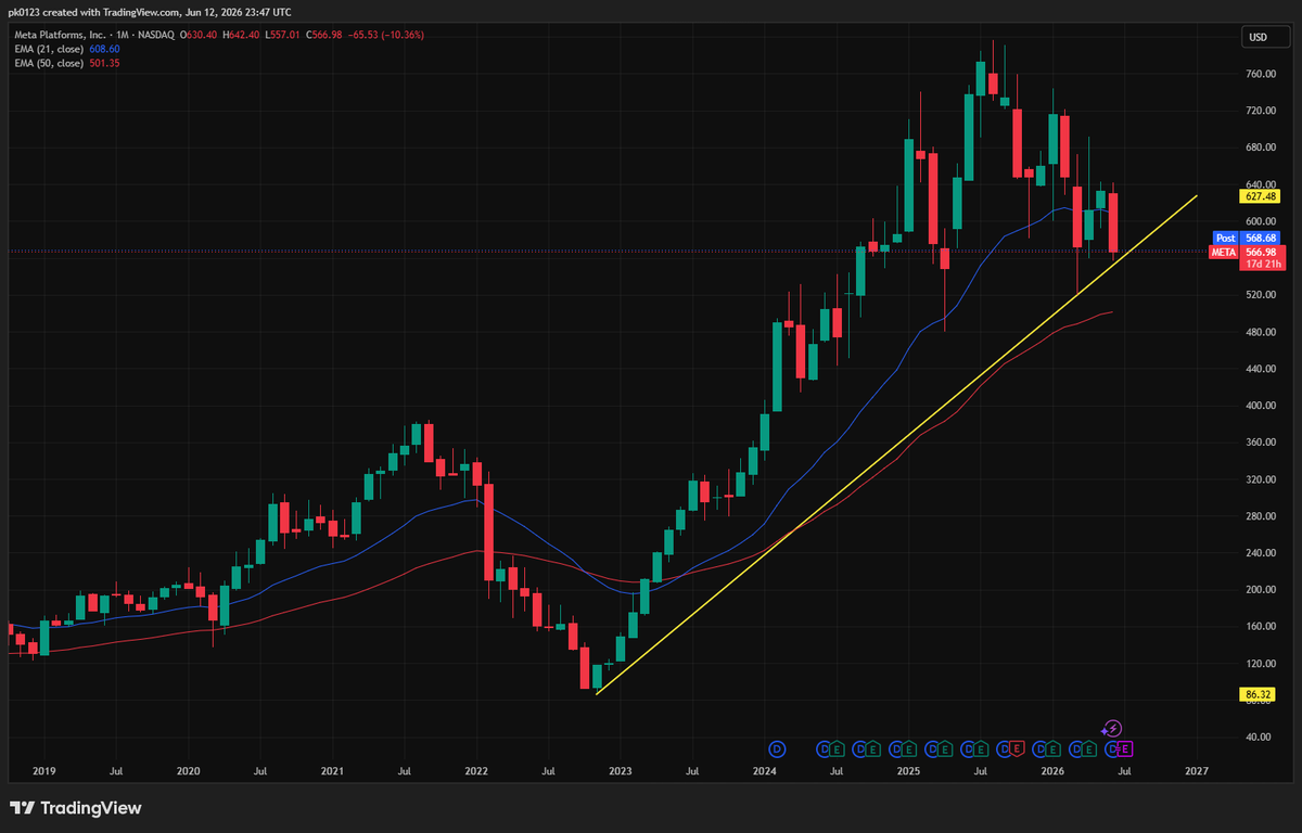
Bought Rocket Lab at $104. Watching META & AMZN.
1
94
Alpha Hunter retweeted
🚀 We're hiring!
Join Sivers Semiconductors and help develop the next generation of SatCom, 5G, 6G, Photonics & Silicon Photonics technologies.
We're looking for experienced Custom IC Layout Engineers with expertise in RF & mmWave IC layout, verification, and full-chip integration.
For more details and to apply, visit: sivers-semiconductors.com/ca…
#Hiring #RFIC #MMWave #Semiconductors #Photonics #5G #6G #SatCom #EngineeringJobs

14
33
520
65,499
Jun 12
I have $4K to go all IN, Shall I full port into SpaceX at open?
3
3
57