
Joined January 2017
- Tweets 10,778
- Following 4,198
- Followers 1,906
- Likes 754
7,048 Photos and videos


Jun 13
Ever wondered how hundreds of electronic connections get soldered in just seconds? ⚡
The answer: Wave Soldering.
A tried-and-true manufacturing process that delivers fast, consistent, and reliable solder joints—specifically for through-hole PCB assemblies.
✅ Simple in concept
✅ Critical in production
When speed and quality matter, wave soldering gets the job done.
#WaveSoldering #PCBAssembly #Electronics #Manufacturing #Engineering #Technology #PCB #PCBA #ElectronicsManufacturing
63
Jun 3
Transparent glass circuit board, saying goodbye to the bulkiness and obstruction of traditional circuits, making technology visible. #RayPCB #TransparentCircuitBoard #TransparentGlassCircuitBoard #PCB #MedicalBeauty #CircuitBoardFactory #pcbmanufacturer #PCBA
61
Jun 2
Why does a MOSFET need a gate resistor if the gate draws no DC current?
Great question. And a common trap.
A MOSFET gate is a capacitor. It draws zero DC current. So in theory, you could drive it straight from an MCU pin.
❌ Wrong. And here’s why:
That capacitor fights you.
A typical MOSFET has Ciss = 1,000–10,000 pF. To switch it, you must charge/discharge that cap fast.
Peak switching current:
I = Ciss × (dV/dt)
Example:
Ciss = 5,000 pF, switching 0–10V in 50 ns → I_peak = 1 A
An MCU pin gives you 20–40 mA. That’s ~25x too weak.
Result? Slow switching → MOSFET lingers in linear region → heats up.
So why ADD a resistor that slows switching?
Because too fast also hurts:
🔔 Ringing – gate oscillations can exceed V_GS(max) and destroy the FET
📡 EMI – fast edges turn your circuit into a radio transmitter
💥 Shoot-through – in half-bridges, both FETs on at once = bang
The gate resistor is a trade-off – switching speed vs. ringing & EMI.
Look at this BSS138K LED switch circuit (image attached).
Two resistors on the gate. Beginners often confuse them.
🔹 R1 = 100Ω (series with gate)
→ The actual gate resistor. Limits inrush current, controls dV/dt.
Skip it → MCU pin stress EMI problems.
🔹 R2 = 10kΩ (gate to GND)
→ This is a pull-down, not a gate resistor.
Holds gate low when MCU pin is floating (reset, power-up, MCU off but 5V present).
Skip it → LED glows randomly during boot or won’t turn off completely.
Both cost < $0.01. Both save hours of debugging.
Now a question for experienced designers:
If CNTRL_MOSFET comes from a gate driver IC (UCC27517, IR2104) instead of an MCU pin:
❓ Is R1 = 100Ω still right? Or too high now?
❓ Does R2 = 10kΩ still matter if the driver has internal pull-down?
Too many reference designs blindly reuse MCU values with gate drivers. They shouldn’t.
What gate resistor value do you use?
And if you’ve used a gate driver IC — did you change R1/R2, or just copy your MCU design?
Let’s compare notes. 👇
2
96
Jun 2
The semiconductor industry still frames EV power electronics as a battle between SiC and GaN.
That narrative is already outdated.
The real question isn’t which wide-bandgap technology "wins."
It’s which technology makes the most sense at each architectural layer of the vehicle.
Why? Because modern EVs are no longer just power electronics systems.
They’re becoming power connectivity optimized systems.
Most conversations around wide-bandgap focus heavily on traction inverters. But outside of high-power traction, the optimization priorities shift fast:
⚡ Switching frequency
🌡️ Thermal efficiency
📐 Form factor
📦 Passive size and weight
🔁 System-level efficiency
This is where GaN becomes extremely compelling — especially in:
Onboard chargers (OBCs)
DC-DC converters
Auxiliary power systems
Zonal architectures
Wireless charging
GaN’s advantages are clear: faster switching, smaller magnetics, higher power density, and compatibility with existing silicon manufacturing infrastructure.
Meanwhile, SiC remains the dominant choice where high voltage and high power matter most:
Traction inverters
Demanding thermal environments
High-performance drivetrains
So here’s how I see it:
SiC dominates the inverter.
GaN quietly (but quickly) expands across most of the remaining EV power stack.
The future isn’t “SiC vs GaN.”
It’s architectural segmentation.
And I believe the industry is underestimating how fast this shift is happening.
#Semiconductors #GaN #SiC #PowerElectronics #EV #WideBandgap #ElectricVehicles
39
May 31
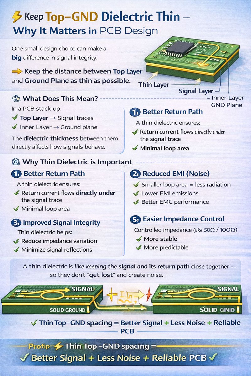
⚡ Why Keeping the Top-to-Ground Dielectric Thin Is a Game-Changer in PCB Design
A small design decision can have a huge impact on signal integrity:
👉 Minimize the distance between your PCB’s Top Layer and the Ground Plane.
🔹 What Does This Mean?
In a typical PCB stack-up:
Top Layer = Signal traces
Inner Layer = Ground plane
The dielectric thickness separating these layers profoundly influences signal behavior.
⚙️ Why a Thin Dielectric Matters
1️⃣ Better Return Path
• Return currents flow right beneath the signal trace
• Smaller loop area
👉 Result: Cleaner, more direct signal paths
2️⃣ Reduced Electromagnetic Interference (EMI)
• Smaller loop area means less radiated noise
• Improves overall electromagnetic compatibility (EMC)
3️⃣ Enhanced Signal Integrity
• Reduced impedance variation
• Minimized signal reflections
• Stable and reliable signal transmission
4️⃣ Lower Inductance
• Ground plane closer to signal traces lowers parasitic inductance
• Boosts high-speed performance
5️⃣ Easier and More Predictable Impedance Control
• Precise impedance targets (e.g., 50Ω or 100Ω) are easier to achieve
• Improves signal quality and design confidence
⚠️ Risks of a Thick Dielectric
• Poor return current paths
• Increased EMI emissions
• Signal distortion and degraded quality
• More crosstalk between traces
💡 Practical PCB Design Tip
Aim for a thin dielectric (~0.1mm - 0.2mm) between your Top Layer (signal) and a solid Ground Plane. Always verify stack-up specs with your manufacturer to ensure optimal performance.
🧠 Quick Analogy
A thin dielectric keeps your signal and return path close — like travel companions who don’t get lost and keep noise at bay.
🔑 In Summary
Thin Top-to-Ground spacing = cleaner signals reduced noise improved reliability
69
May 30
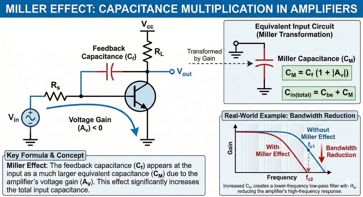
⚡ Mastering the Miller Effect: A Key Challenge for Today’s High-Speed Engineers
What is the Miller Effect?
It’s the phenomenon where feedback between amplifier input and output nodes multiplies the equivalent input capacitance, often limiting performance.
The Science Behind It
High voltage gain makes this parasitic capacitance appear much larger, creating a bottleneck that slows down circuit switching speeds.
How Engineers Tackle It
Microprocessor designers optimize designs to push clock speeds higher.
Telecom experts use cascode amplifier topologies to minimize signal distortion.
Electric vehicle inverter teams carefully manage gate drive techniques for optimal performance.
The Bottom Line:
Effectively controlling parasitic capacitances like the Miller effect is critical for maintaining reliable, high-frequency electronic operation in advanced technology applications.
5
96
3,538
May 29
Here’s a straightforward visual guide to mastering soldering techniques and troubleshooting common challenges.
Recognizing the difference between a solid solder joint, a cold joint, and a dry joint is crucial for ensuring the reliability and quality of any electronic assembly.
This infographic breaks down essential best practices to enhance your soldering outcomes and helps you avoid frequent pitfalls like poor wetting, inadequate heat application, and unclean surfaces.
45
May 29
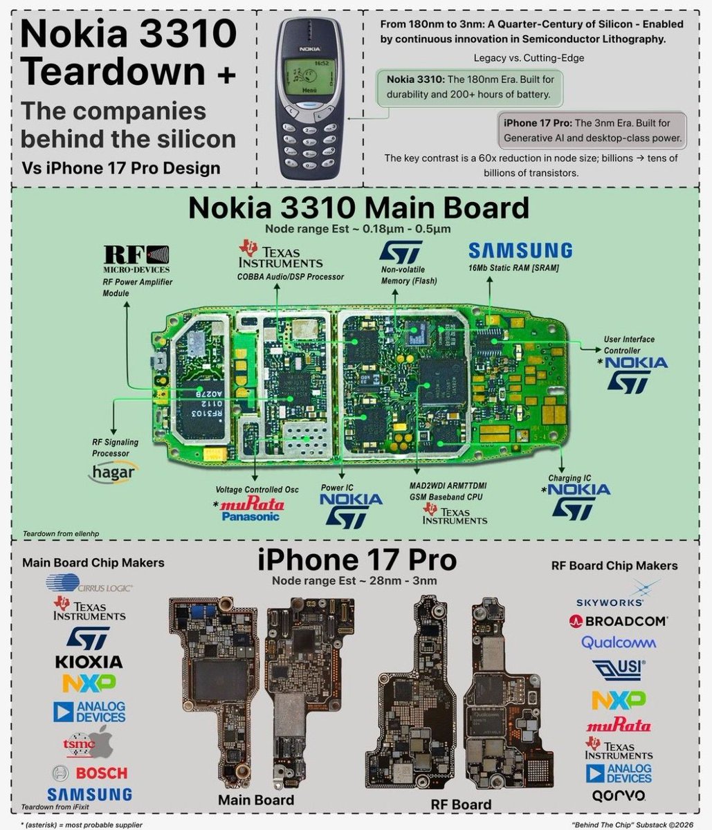
🚀 From the iconic Nokia 3310 to the cutting-edge iPhone 17 Pro:
How STMicroelectronics Has Powered 25 Years of Mobile Innovation
Did you know the legendary Nokia 3310 — famed for its unmatched durability and over 200 hours of battery life — shares a vital connection with today’s powerhouse, the iPhone 17 Pro? It’s STMicroelectronics, the silent force driving mobile technology for a quarter-century! And now, ST is powering the future of AI-enabled devices.
A Journey Through Innovation:
2000 – The Nokia 3310 Era:
Built on 180nm silicon nodes focused on durability and exceptional battery life
STMicroelectronics supplied critical components including non-volatile Flash memory, audio amplifiers, and power management ICs — the unsung enablers of the 3310’s legendary resilience
Fun fact: The 3310’s MAD2WDI ARM7TDMI CPU was revolutionary in its time!
2024 – The iPhone 17 Pro Era:
Shift to advanced 3nm silicon nodes, powering AI generation and desktop-class performance in your pocket
ST continues to innovate with contributions in RF modules, power management, and cutting-edge sensors that make the iPhone 17 Pro a true powerhouse
Why This Matters:
From billions to tens of billions of transistors, STMicroelectronics has led the charge in miniaturization, efficiency, and performance
ST’s technology powers critical yet invisible elements—charging ICs, voltage-controlled oscillators, RF processors—that keep your device alive and connected
Collaboration with industry leaders drives innovation further, pushing the boundaries of what mobile technology can achieve
Looking Ahead:
As we step into an era defined by AI-driven smartphones, IoT integration, and 6G connectivity, STMicroelectronics remains at the heart of innovation. The next generation of groundbreaking devices will almost certainly bear ST’s mark.
Let’s celebrate the unsung innovators behind the tech we rely on every day!
Drop a 🚀 if you still remember your Nokia 3310 fondly, or tag someone who should know about the hidden giants powering today’s smartphone revolution.
1
4
133
May 29
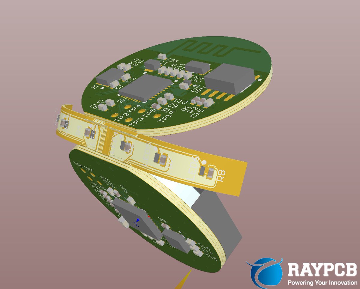
Teardown of 5G 5th Generation Mobile Communications Test System RF Module Keysight, a technology from IDEXX The oscillator module utilizes Rogers ceramic layer
1
105
May 28
Essential Microcontrollers Every Engineer & Tech Enthusiast Should Know 🧠⚙️
From smart IoT devices to advanced robotics and automation systems — microcontrollers are the silent brains behind it all.
If you're diving into electronics or embedded engineering, here are some of the most popular and versatile platforms to add to your toolkit:
🔹 Arduino UNO – Perfect for beginners and rapid prototyping
🔹 ESP32 – Built-in Wi-Fi & Bluetooth for IoT projects
🔹 Raspberry Pi Pico – Affordable, powerful, and flexible
🔹 STM32 – High performance for professional applications
🔹 PIC – Reliable and widely used in industrial settings
🔹 MSP430 – Ultra-low power for battery-operated devices
🔹 ESP8266 – The classic choice for Wi-Fi-enabled projects
🔹 ATtiny85 – Small but mighty for compact designs
Getting familiar with these microcontrollers opens up endless possibilities — from hobbyist builds to cutting-edge innovation.
Which one is your go-to? Drop your favorite in the comments 👇
#Microcontrollers #EmbeddedSystems #IoT #ElectronicsEngineering #TechEnthusiast

11
57
1,446