
making things happen with electron microscopes🔬 she/her 🐘: chaos.social/@isabel 🦋: bsky.app/profile/beamshift.b…
Joined March 2022
- Tweets 757
- Following 1,838
- Followers 1,552
- Likes 14,412
223 Photos and videos


Isabel retweeted

Jun 7
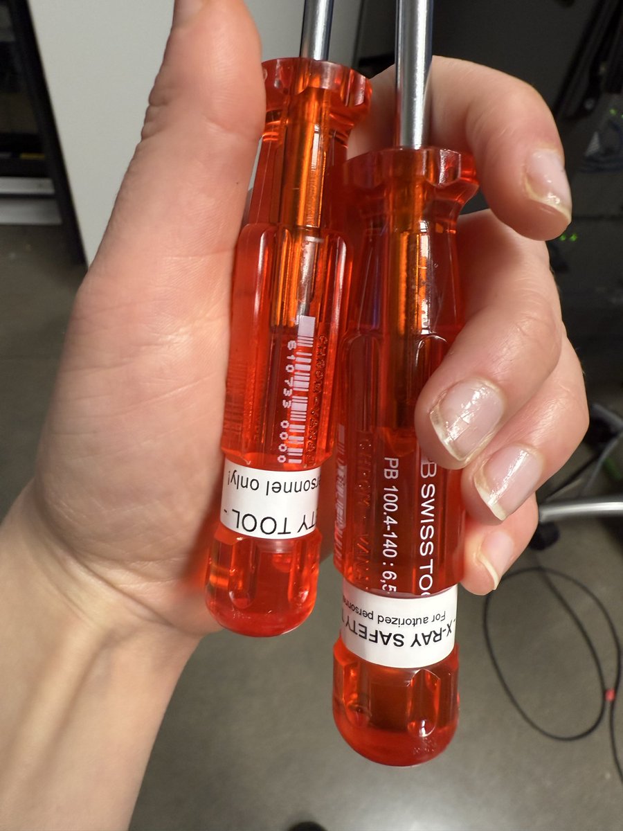
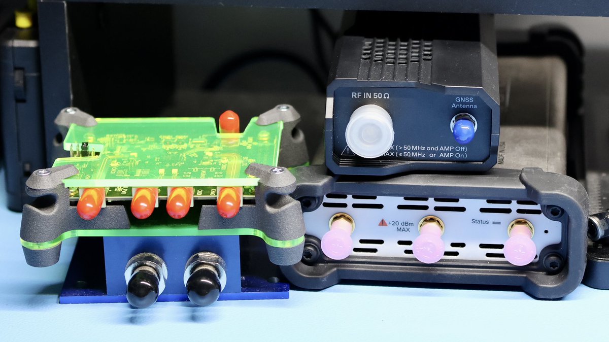
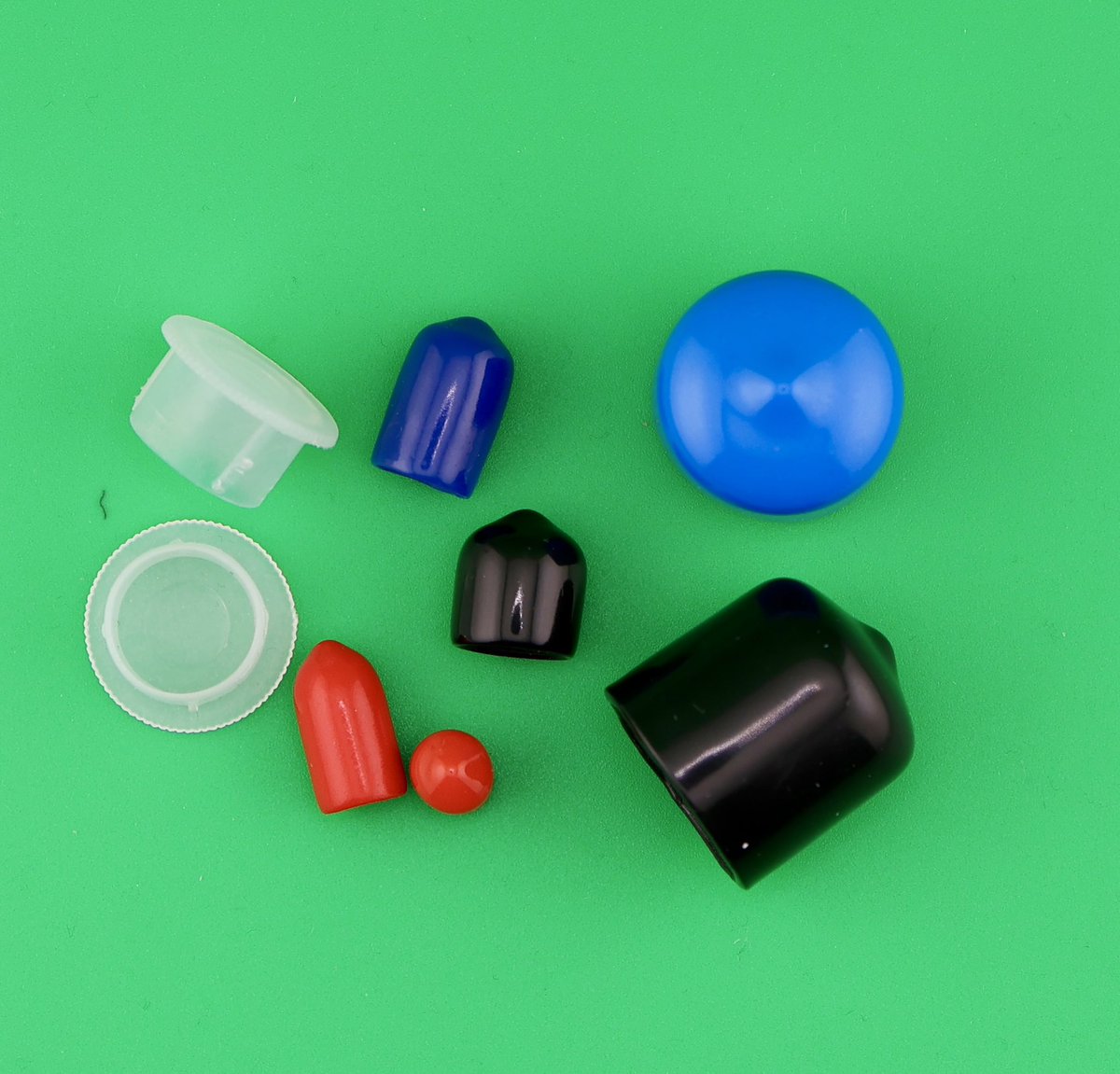
Reminder: protect the connectors on your precious RF tools and SDRs when you are not using them.
Usually called dust caps, they are available for any type of connector you imagine.
9
2
134
5,877
Isabel retweeted

Jun 7
Lithography is the technology, that forces rocks to think by engraving runes.
83
565
6,508
410,399
Isabel retweeted

Jun 7
In 1911, Heike Kamerlingh Onnes, by virtue of being the first person to liquify helium, serendipitously discovered that the resistance of mercury dropped to zero below 4.2K–the first superconductor. For the next decades, some of the luminaries of 20th century physics tackled the superconductivity problem, without achieving the holy grail of a microscopic theory about why it happens. It was not until two smoking gun experiments in the 1950s pointed in the correct direction: isotope effect experiments in mercury showed that the atomic lattice, not just electrons, were implicated, and low-temperature specific heat experiments gave evidence for a small energy gap associated with the superconducting state. These key experiments were among thousands of valid works about superconductivity, and certainly no one knew what would be the smoking gun experiment in 1911 or even in 1941 (the author of the isotope effect paper even stated that their motivation was that they had different isotopes of mercury laying around).
With all the key observations in place, Bardeen, Cooper, and Shrieffer were able to formulate the BCS theory explaining what is now called the ‘conventional’ type of superconductivity.
This history illustrates the important role of serendipity and path-dependence in superconductivity research (as well as other areas dealing with complex many-body systems). If Onnes chose to measure aluminum instead of mercury, he would not have discovered superconductivity when he did; if someone had tried to FAFO superconductivity in different isotopes of a metal earlier, the mechanism of superconductivity could have been established much sooner.
Similarly if superconductivity was discovered in Ba1-xKxBiO3 (BKBO, Tc up to 34K) *before* it was discovered in La2-xBaxCuO4 (LBCO, Tc up to 35K, first cuprate discovered), humanity could have gone another generation without discovering cuprate superconductivity in excess of liquid nitrogen temperatures.
2
9
88
6,289
Isabel retweeted

Jun 6
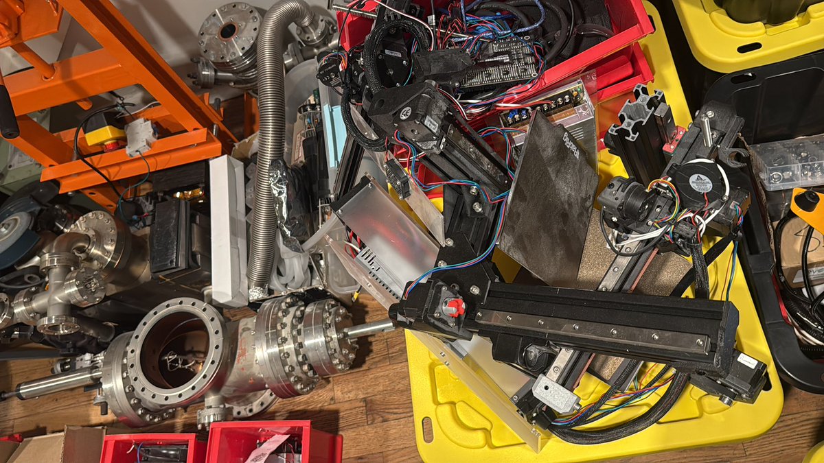
Anyone in nyc enjoy building things and want free gear? 3D printer kits, conflat vacuum chambers, lasers, optics, glassware, electronic test equipment etc . Morningside heights Manhattan dm me
3
7
23
2,225

Isabel retweeted

May 31
tomorrow at 1pm i need skilled hands who have a desire to disassemble extremely cool scientific equipment
if you are in sf and have ever wanted to do something like that please message me and come help
19
8
102
7,731
Isabel retweeted

May 28
From Scotch-tape exfoliation to wafer-scale electronics.
Our improved roll-to-roll mechanical exfoliation method yields homogeneous large-area films of 2D materials like MoS2, WSe2, hBN and graphite. Fully dry and scalable!
Link in the 1st comment 👇
#2Dmaterials #nanotech

8
15
157
154,801
Isabel retweeted

May 23
4
15
857

May 22
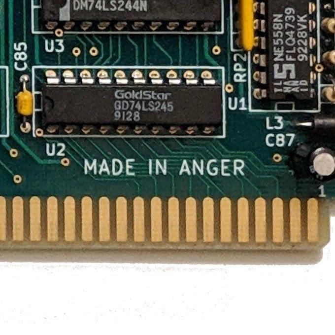
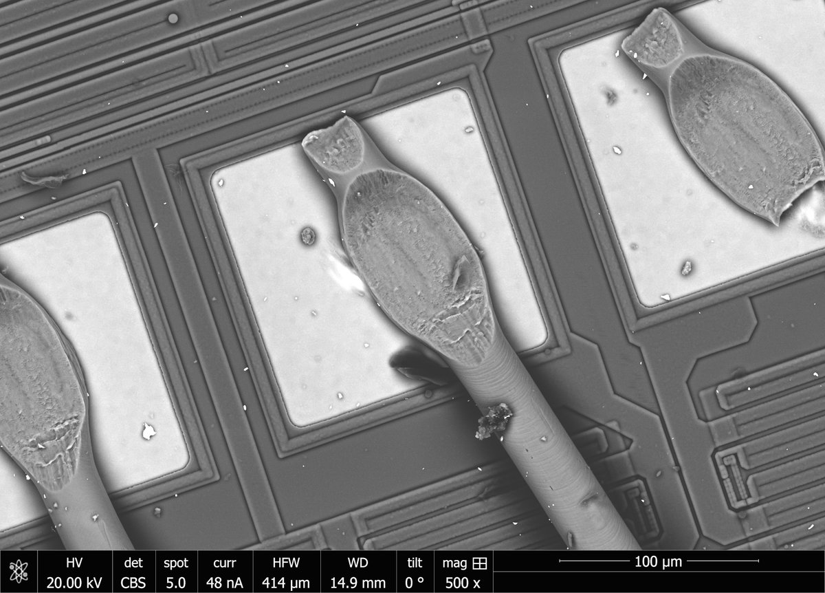
i received an untapped NPT fitting from mcmaster, some would call this a quality control issue but i appreciate pulling a rare variant
2
44
1,350
Isabel retweeted

May 20
I want to share a project I've been working on the past few weeks
Introducing AMADEUS: agent tooling for automated operation of transmission electron microscopes (TEMs)
why did I build this?

3
8
52
8,897
Isabel retweeted

May 7
My new dual-beam SEM - FEI Versa 3D zeptobars.com/en/read/SEM-FE… via @Zeptobars

5
6
64
4,060
May 6
you don’t need to do this unless your son is an electron microscope
May 5

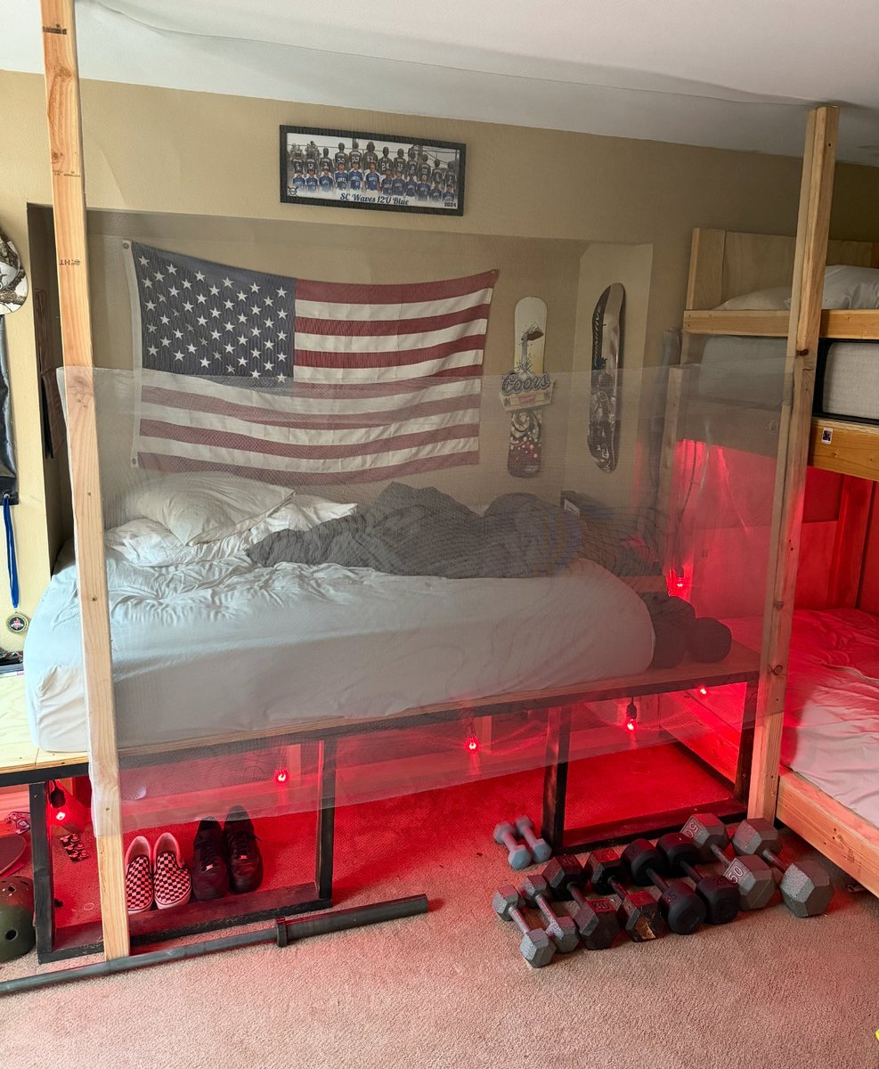
For everyone who asked- This was my temporary “emergency made” faraday that I made around my son’s bed until we moved.
It significantly reduced the radiation from the nnEMF from the 5G tower (~80microwatts)
keeping him protected while he slept was (at a minimum) my priority.
Community note
The claimed nnEMF exposure of ~80 μW/m² from the 5G tower is thousands of times below FCC public safety limits and not linked to adverse health effects. fcc.gov/consumers/guid… who.int/news-room/ques…
77
195
7,502
339,057
May 6
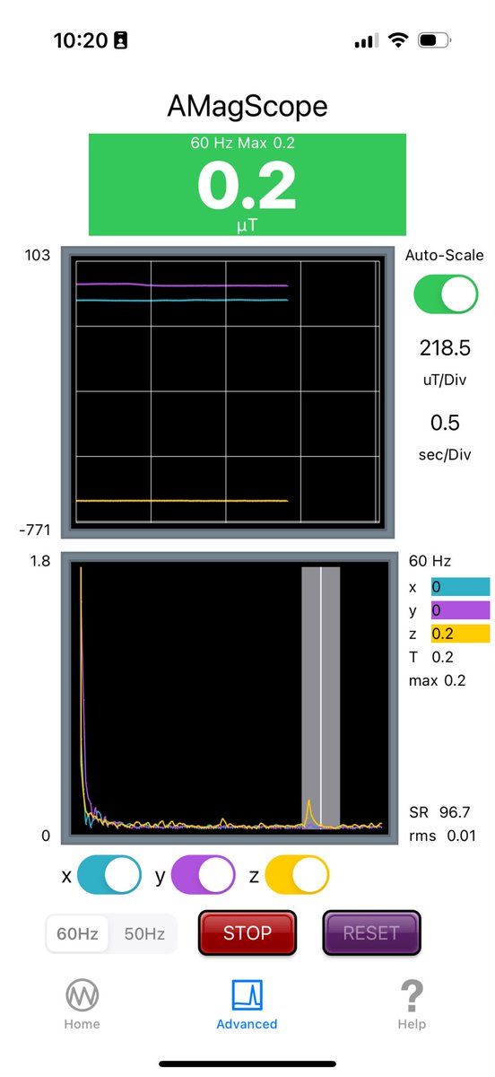
here’s something electron microscopists and crunchy parents can both get behind: the only app that used iPhone magnetometer data to measure 60Hz AC magnetic fields isn’t in the App Store anymore. where did it go? someone should make a new one
3
2
27
3,198
May 6
the iPhone magnetometer tops out at 100Hz but you can work around that with a clever sampling/FFT analysis trick: image-ppubs.uspto.gov/dirsea…
21
2,008
May 6
TIL a liquid metal ion source (LMIS) can be converted into a field emission electron source: rapidly turn off an operating ion source to freeze the Taylor cone into a solid pointy tip and reverse polarity of high voltage. doi.org/10.1116/1.584459
1
3
17
820
Apr 28
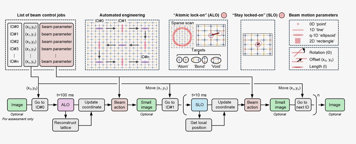
closed loop & vectorized scan control enables some really interesting stuff!
Apr 27

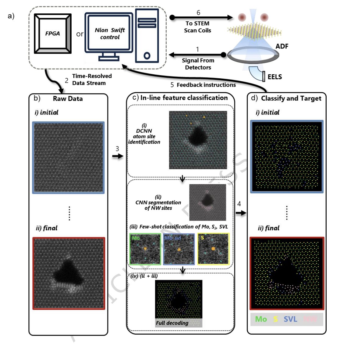
Autonomous atomic-scale fabrication: ML-guided electron beams sculpting 2D materials
Functional properties of 2D materials like MoS2 are exquisitely sensitive to atomic structure. A metallic Mo6S6 nanowire along a hole edge in semiconducting MoS2 yields a 1D-2D heterostructure with electronic behavior nothing like the pristine monolayer. Building this atom by atom means ejecting sulfur atoms at chosen sites, and earlier automated workflows leaned on lucky statistics, with success rates near 64%.
Zijie Wu and coauthors build a fully autonomous platform that closes the loop between imaging, ML, and beam control in a STEM. After each HAADF acquisition, three lightweight models decode the image: a U-net ensemble (ELIT) locates atoms, a second U-net segments collapsed MoS-nanowire regions, and a random forest classifies each site as Mo, S, or sulfur-vacancy-line. The classifier learns from 55 hand-labeled neighborhoods, each encoded by distances and intensity to the 5 nearest atoms. No huge simulated datasets, no GAN style transfer, no foundation model.
Selected sulfur sites go to an FPGA-controlled scan routine that places the beam in Archimedean spirals with radially symmetric dose. Three strategies are shown: targeted nanowire growth along a pore edge, freestanding MoS-NWs between two seed pores, and directional growth using DBSCAN and line fitting on the largest cluster. The directional case reaches 65% success over 42 runs, with decoding in about 1 second on a GPU.
What stands out from an ML-for-science angle is the deliberate small-data philosophy. For atomic labeling, big vision models trained on simulated images often transfer poorly to experiments. Pairing simple models with intuition-based feature engineering is faster to deploy and easier to tune.
For applied R&D in semiconductors, quantum devices, and 2D electronics, this reframes what atomic-scale design means. Teams can specify a target defect topology and let the platform iterate toward it without massive labeled datasets, and the framework should transfer to other TMDs, making it relevant for catalysis, energy materials, and quantum sensors.
Paper: Wu et al., npj Computational Materials (2026) — CC BY 4.0 | doi.org/10.1038/s41524-026-0…
3
8
1,618
Isabel retweeted

Apr 27
Autonomous atomic-scale fabrication: ML-guided electron beams sculpting 2D materials
Functional properties of 2D materials like MoS2 are exquisitely sensitive to atomic structure. A metallic Mo6S6 nanowire along a hole edge in semiconducting MoS2 yields a 1D-2D heterostructure with electronic behavior nothing like the pristine monolayer. Building this atom by atom means ejecting sulfur atoms at chosen sites, and earlier automated workflows leaned on lucky statistics, with success rates near 64%.
Zijie Wu and coauthors build a fully autonomous platform that closes the loop between imaging, ML, and beam control in a STEM. After each HAADF acquisition, three lightweight models decode the image: a U-net ensemble (ELIT) locates atoms, a second U-net segments collapsed MoS-nanowire regions, and a random forest classifies each site as Mo, S, or sulfur-vacancy-line. The classifier learns from 55 hand-labeled neighborhoods, each encoded by distances and intensity to the 5 nearest atoms. No huge simulated datasets, no GAN style transfer, no foundation model.
Selected sulfur sites go to an FPGA-controlled scan routine that places the beam in Archimedean spirals with radially symmetric dose. Three strategies are shown: targeted nanowire growth along a pore edge, freestanding MoS-NWs between two seed pores, and directional growth using DBSCAN and line fitting on the largest cluster. The directional case reaches 65% success over 42 runs, with decoding in about 1 second on a GPU.
What stands out from an ML-for-science angle is the deliberate small-data philosophy. For atomic labeling, big vision models trained on simulated images often transfer poorly to experiments. Pairing simple models with intuition-based feature engineering is faster to deploy and easier to tune.
For applied R&D in semiconductors, quantum devices, and 2D electronics, this reframes what atomic-scale design means. Teams can specify a target defect topology and let the platform iterate toward it without massive labeled datasets, and the framework should transfer to other TMDs, making it relevant for catalysis, energy materials, and quantum sensors.
Paper: Wu et al., npj Computational Materials (2026) — CC BY 4.0 | doi.org/10.1038/s41524-026-0…
10
29
2,758


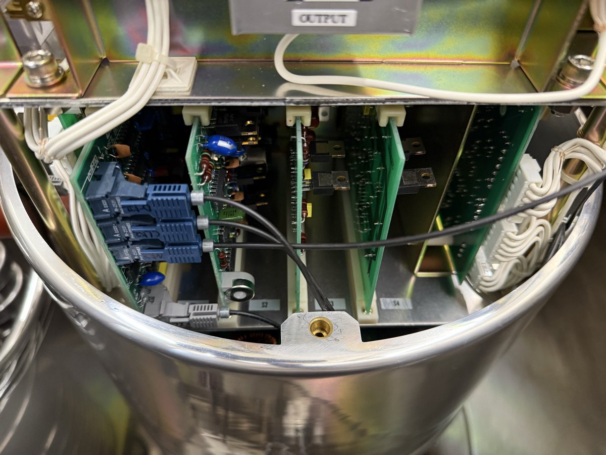
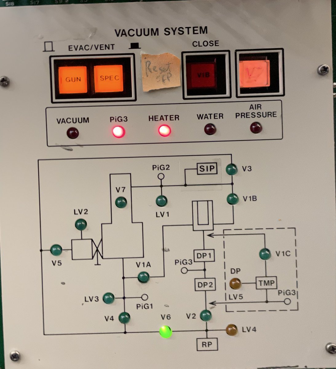
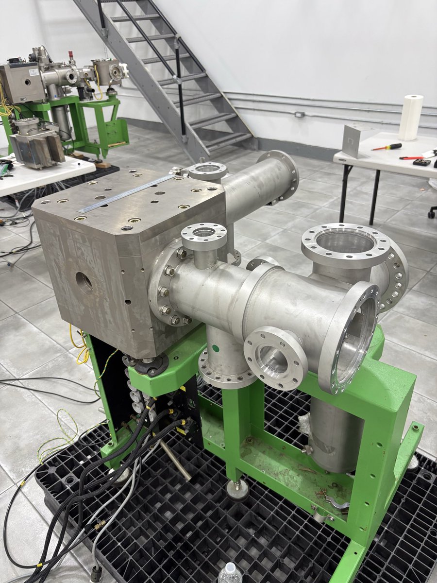
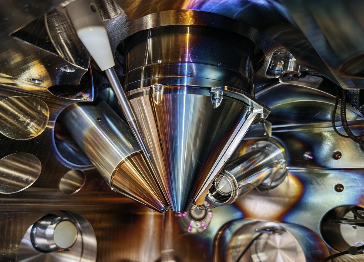
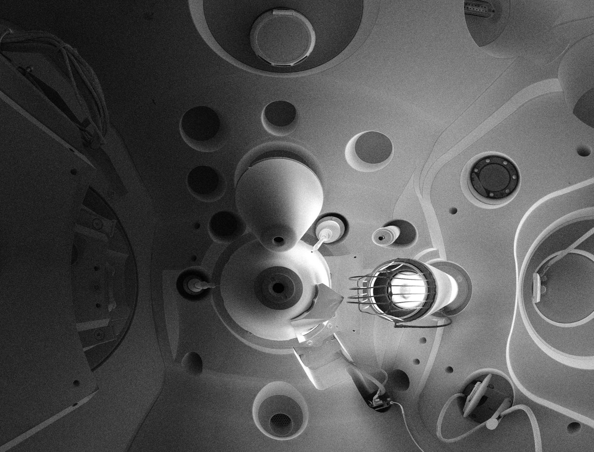
Apr 14
do u like vacuum systems? i uploaded some photos of the electron microscope i’m working on and then i labeled them and made it interactive. beamshift.net/2100F Vacuum…
1
3
20
927
Isabel retweeted
Apr 9
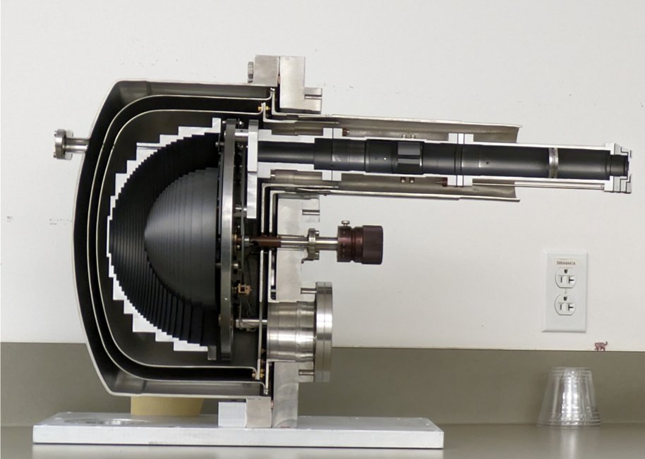
If you have the means, you should always cut old scientific instruments in half. Below is a cross-section of an old-school photoelectron analyzer, from the Advanced Lightsource.
5
9
91
3,812