
19 Nov 2025
إذا كان عليك الاختيار: هل تفضّل هاتفاً بسطوع “أرقام قياسية”؟ أم شاشة ذات انعكاس منخفض تمنحك رؤية حقيقية تحت الشمس؟
شارك رأيك.
#SmartphoneDisplay #Brightness #AntiReflection #TechTwitter
6
2,127

29 Oct 2025

11
1,332

19 Oct 2025
Highlights
•
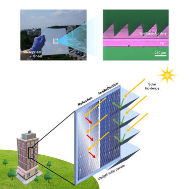
Wedge microprisms yield omnidirectional antireflection for upright solar panels
•
Surface reflectance below 1% for direct sunlight in the daytime is achieved
•
An enhanced photovoltaic efficiency of ∼15% is observed in real-world settings
•
Applications for building integration, vehicles, and solar farms are expected
sciencedirect.com/science/ar…
2
6
423

16 Oct 2025
I went to the local mobiles store to ask if they have any antiglare/antireflection screen protectors for 17 Pro Max. They were trying to sell me the privacy protector even after explaining it’s a different thing and not what I am after. Grandparents would probably have bought it
1
15
8,292

1 Oct 2025
🧵 3/12
#Solar Cell Structure - #Engineering #Marvel:
🛡️ Antireflection Coating - Minimizes light reflection
⚡ Top Junction Layer - Creates electric field
💎 Absorber Layer - Core #silicon where magic happens
🔌 Metal Contacts - Grid pattern to collect electricity
🏗️ Back Contact - Completes the electrical circuit
Fun Fact: Front contacts are thin grid lines to let maximum light through while still collecting current efficiently!
1
5
25

25 Sep 2025
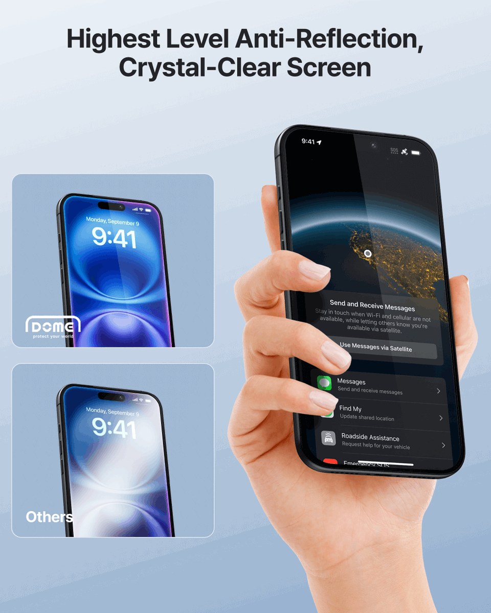
AR DOME GLASS for iPhone 17 – Premium screen protection with Anti-Reflection!
>
17: amazon.com/dp/B0FPLSLYJH
17 Pro: amazon.com/dp/B0FPVZCJL3
17 Air: amazon.com/dp/B0FPWVWF8K
17 Pro Max: amazon.com/dp/B0FPWMY2KT
>
#iPhone17 #DomeGlass #Whitestone #AntiReflection #TemperedGlass
1
2
119

11 Sep 2025
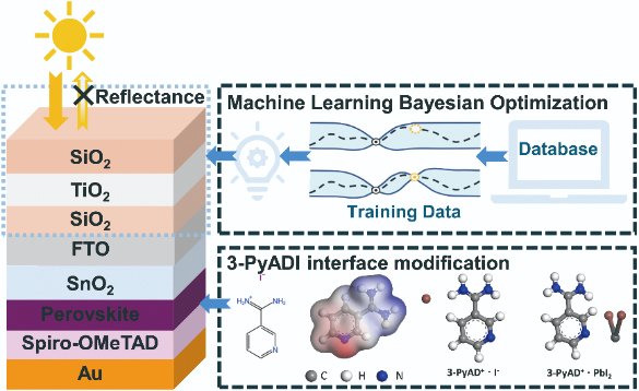
Machine learning-guided antireflection coatings architectures and interface modification for synergistically optimizing efficient and stable #perovskite solar cells sciencedirect.com/science/ar…
#AI #AIchem @PerovskiteTweet @perovskiteinfo
1
4
14
555

9 Sep 2025
There's footage of the phones already and they definitely don't resemble the Galaxy Ultra's antireflection. (This is a 17 Pro)

2
39
2,936

10 Aug 2025
[PDF] Learning deeply to vanish light: intelligent metasurface design for next-generation antireflection 🛸✈️ goo.gl/scholar/D2Xm7e
1
2
45

8 Mar 2025
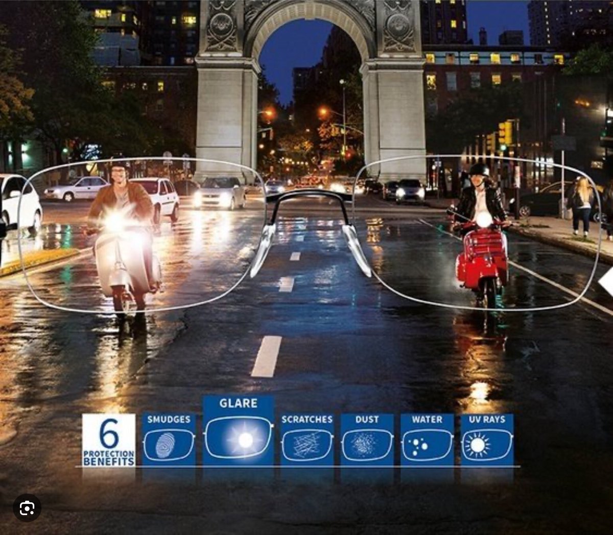
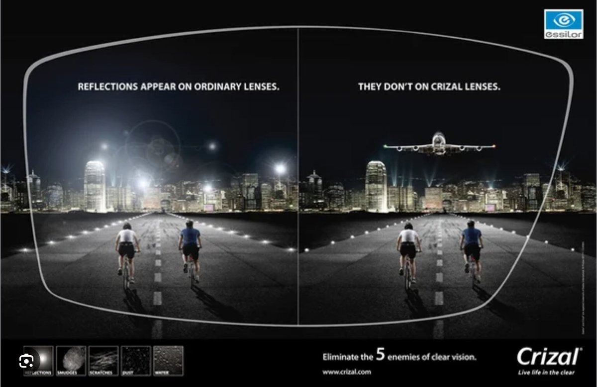
💎 #Sapphire wonder material.
Sapphire mineral is a crystalline form of aluminum oxide (Al₂O₃) with hexagonal molecular structure. Sapphire is largely used in the manufacturing industry for a unique combination of properties that range from the hardness which is one of the highest in nature, 9 in the Mohs scale, to the density at approx 3.98 g/cm³. Sapphire has elevated refractive index, excellent shock resistance, and a compressive strength that reach up to 2,000 MPa which makes this mineral highly resistant to heat, wear and erosion. Last but not least sapphire has exceptional dielectric properties making it the ideal substrate for electronics such as LEDs, lasers, and semiconductor or simply as electrical insulator.
In this nano engineering work is reported the fabrication of sapphire nanostructures with a tapered profile displaying scratch free, anti-glare, anti-fogging, and anti-dust protection. The composition is made by nanopillars spaced 330 nm apart and an aspect ratio of 2.1. The sample exhibit broadband and omnidirectional antireflection qualities, with an enhanced light transmission of 95.8% at λ of 1360 nm, the highest reported for sapphire thus far.
🔗 pubs.rsc.org/en/content/arti…
5
23
115
3,656

7 Mar 2025
Sapphire nanostructures for electronic displays.
You'd think these would be problematic, but this paper is saying it's dirt resistant due to extreme hydrophobicity, and it's even scratch, fog & glare resistant. The full patterning process is explained:
"The nanostructures were patterned using interference lithography, and then transferred to a sapphire substrate using reactive ion etching. Sapphire has a low etching rate due to its chemical stability, and thus a thick polysilicon layer with a thickness of 1000 nm was deposited on the sapphire substrates for use as an etching mask. Subsequently, the samples were spin coated with a 100 nm-thick antireflection coating (Brewer Science, ARC i-con-7) and 200 nm-thick photoresist (Sumitomo, PFi-88A2). The photoresist was exposed using a Lloyd's mirror interference lithography (Kimmon HeCd laser, 325 nm wavelength) to pattern a 2D pillar array with a period of 330 nm. The photoresist pattern was transferred into the underlying ARC, polysilicon, and sapphire substrates using inductively coupled plasma reactive ion etching (ICP, Oxford 100) using O2, HBr, and BCl3/HBr gases, respectively. Notably, a low-RF power was used for the etching of the polysilicon layer with HBr RIE, which significantly increased the silicon to photoresist etch selectivity."


2
1
30
2,406

21 Feb 2025
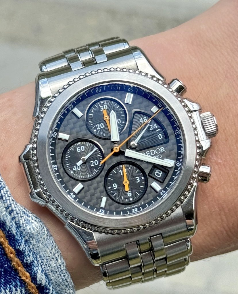
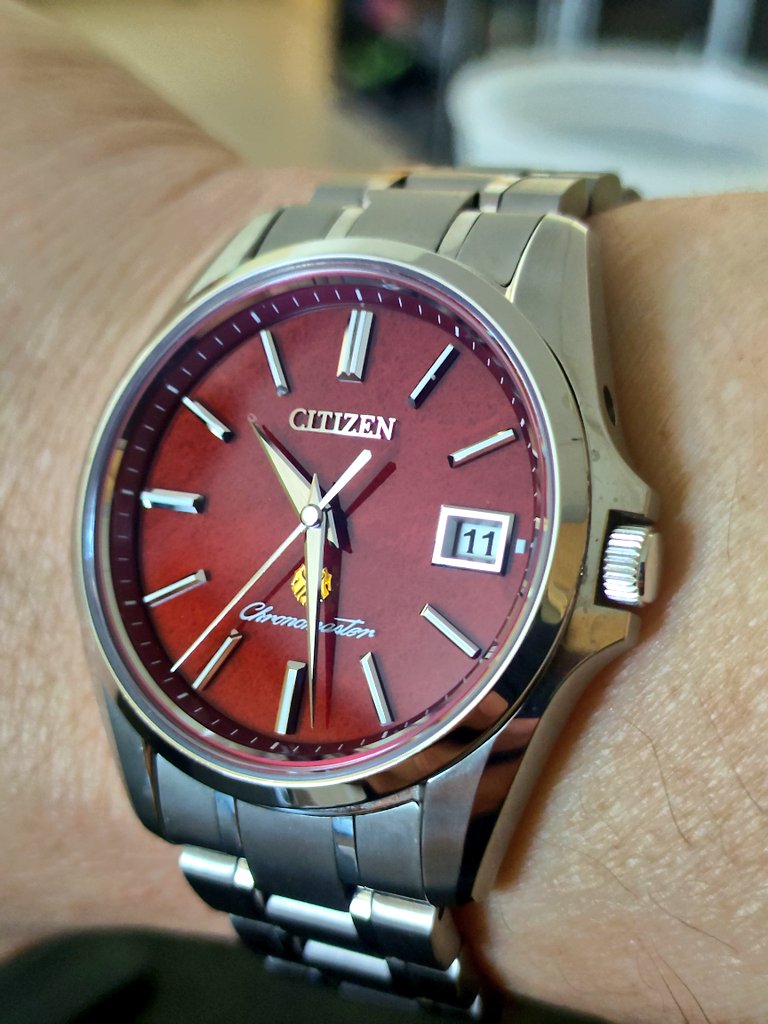
Lol they don't know what is antireflection coating... You will soon have one way mirror where the hands look at you!!
This is anti reflecting coating from good Japanese watches

1
107

29 Jan 2025
Best display not there are other display that is better in antireflection yes
1
37
6,716

28 Jan 2025
Antireflection matters 👋
27 Jan 2025

Screen Reflection Test !
Left : Samsung S25 Ultra
Right : Oneplus 13
Which one is better?
1
13
612

18 Jan 2025
Gu2025: Bioinspired broadband antireflection coatings on silicon wafers enabled by a polyimide-assisted self-masking technique
doi.org/10.1364/OL.540303
6
340

The top QD-OLED will put out about 4,000 nits, has an improved antireflection screen, and the AI processor went from 20 neural processing units to 120 neural processing units. Processing was always one of the weaker aspects of Samsung's tvs so it should massively improve picture.
1
66


9 Nov 2024
We all love using our collections to talk about structural color! 🦋
Time for a physics lesson now as @americanbeetles provides some of her
favorite methods for demonstrating circular polarization, pointillistic color
mixing, diffraction gratings, antireflection & more! #ECN2024
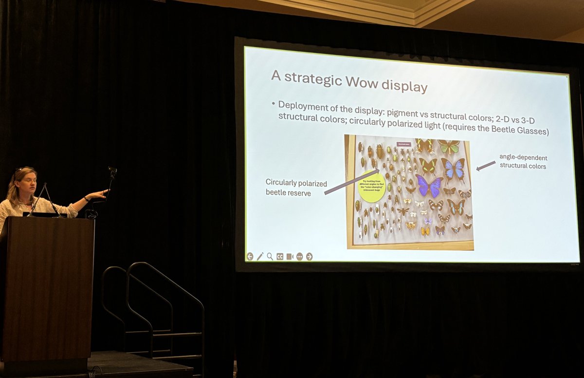
3
24
759