
Jun 12
Green MBA Careers: How Sustainability is Creating Business Opportunities
Explore more: icfaibytes.in/green-mba-care…
#greenMBA #SustainabilityCareers #ecofriendlybusiness #blog #sustainablejobs #greenbusiness #mbaforchange #blogarticle #ICFAIOnlineMBA #CareerInSustainability

3

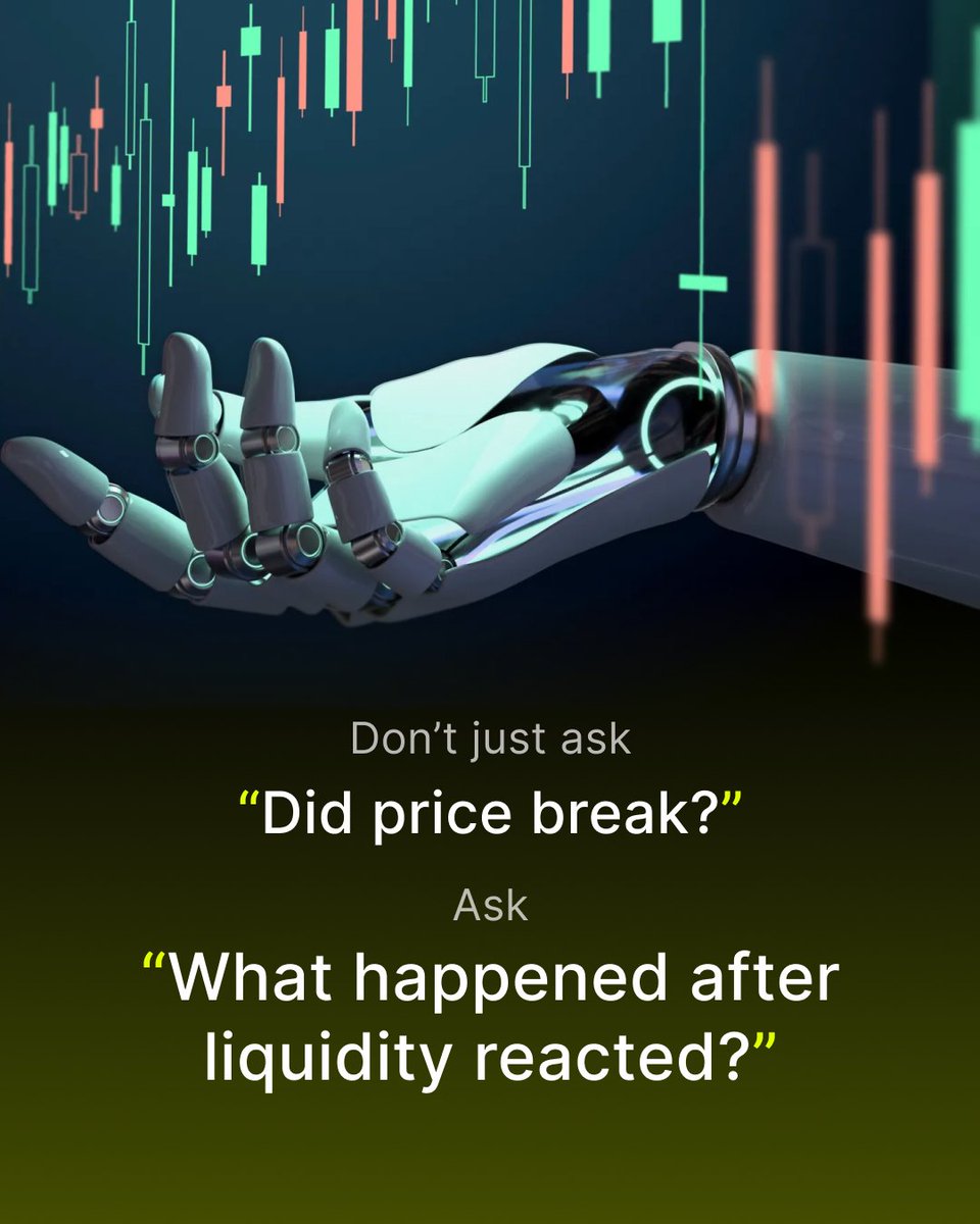
Jun 10
🔍 One thing standing out right now:
The first move after headlines or data releases is not always the real move.
We’re seeing:
→ Crude spikes fade
→ Treasury reversals
→ ES reclaim failed breakdowns
→ NQ continue only after controlled pullbacks
Patience is becoming part of edge again.
Read more: f.mtr.cool/muctupigkt
#blog #blogarticle
1
300

Charting Excellence in Trimaran Engineering. The quest for the ultimate small cruising trimaran has reached its destination.
Read the full article on blog.theboatdb.com/best-smal… and sail to the future with knowledge.
#marinedatacloud #theboatapp #theboatdb #Blogarticle

8
Jun 9
The real debate is this: when a clean level gets swept and reclaimed, do you trust the original structure less… or the reaction after liquidity gets taken?
Curious how other traders think about this.
Read more: f.mtr.cool/vwrxddlfld
#blog #blogarticle
1
209
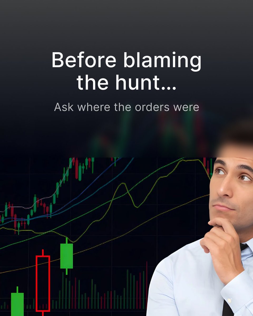
Jun 9
You place your stop below a clean low.
Price tags it perfectly… then reverses without you. 😤
That’s usually the moment traders say:
“Yeah, they were clearly hunting stops.”
#blog #blogarticle
2
2
537
Jun 8
👀 One of the biggest mindset shifts for breakout traders:
A level break is NOT confirmation.
The reaction after the break matters more than the break itself.
That is where Level II and order book skew can change the read completely.
Read more: f.mtr.cool/tyshbyject
#blog #blogarticle
1
297
Jun 8
🚨 A lot of low-timeframe breakout failures are visible before the reversal even starts.
Price breaks the level…
…but the order book never truly supports the move.
That is the trap.
#blog #blogarticle
1
8
790

With our new chemical warehouse in Bremen, we’ve built an infrastructure that simplifies complexity while strengthening control, flexibility and transparency across the supply chain. Discover more in our latest #blogarticle: monkeylink.co/322f35

12
Jun 2
📉 Market update:
One of the biggest disconnects in trading is this:
Price can look strong on the chart… while liquidity underneath is getting weaker
That’s usually where traders get trapped
#blog #blogarticle
1
7
964
May 28
Don’t just ask “Where is price going?”
Ask “What is liquidity doing as price gets there?”
Read more: f.mtr.cool/tbyzxmayos
#blog #blogarticle
2
247
May 28
A candle can tell you price moved.
It won’t tell you what happened *inside* the move. 👀
Was liquidity waiting there?
Did orders pull away?
Did aggressive buyers get absorbed?
That’s the part most traders miss.
#blog #blogarticle
1
5
636
May 27
🌍 Market update: headlines are moving fast
Energy risk. Central banks. China growth signals. Market structure shifts.
For traders, the question is not “what happened?” It’s: what changed?
#blog #blogarticle
1
4
546
May 26
📍Market update: traders aren’t just watching candles anymore.
More traders are tracking liquidity directly: where large orders sit, disappear, absorb, or get hit before price reacts.
That’s a very different view of the market.
#blog #blogarticle
1
2
6
446
May 25
🌍 Market update: headlines are moving fast:
Energy risk
Central banks
China growth signals
Market structure shifts
For traders, the question is not “what happened?” It’s: what changed?
#blog #blogarticle

1
4
584

May 25
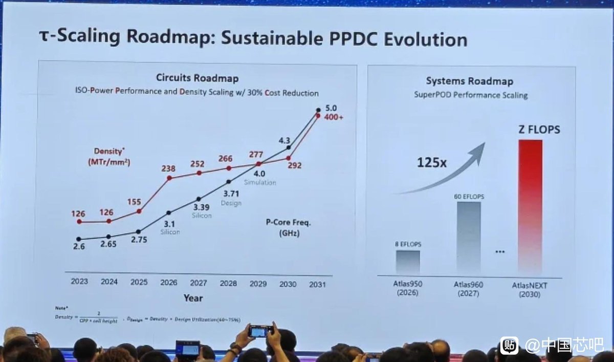
Chinas Huawei can't access EUV. So they wrote their own scaling law. The leverage of US export controls erodes.
Huawei just presented the Tau (τ) Scaling Law at IEEE ISCAS, a framework that replaces geometric transistor scaling with time-based optimization across devices, circuits, chips, and systems.
Huawei is not trying to win the nanometer race anymore. They're redefining it.
381 chips designed and mass-produced over six years. Kirin chips with their new LogicFolding architecture ship this fall. Target by 2031: transistor density equivalent to 1.4nm processes - without EUV (ASML embargo still hits hard)
Whether Tau Scaling delivers on that promise remains to be seen. But it shows one thing: US export controls cut Huawei off from cutting-edge lithography, and instead of hitting a wall, they built a parallel road.
China's semiconductor independence isn't hypothetical anymore. It's shipping in phones, running AI workloads, and now has its own scaling law presented at one of the world's top circuit design conferences.
If Huawei can close the performance gap through architecture instead of lithography, the entire leverage of US export controls erodes. The sanctions were designed to keep China two generations behind. Huawei is trying to make that metric irrelevant.
h/t @AndrewCurran_ for finding this interesting blogarticle and @zephyr_z9 for the photo

May 25

Huawei says it has made a breakthrough and expects to design high-end chips with transistor density equivalent to 1.4 nm processes by 2031.

38
81
563
60,717
May 22
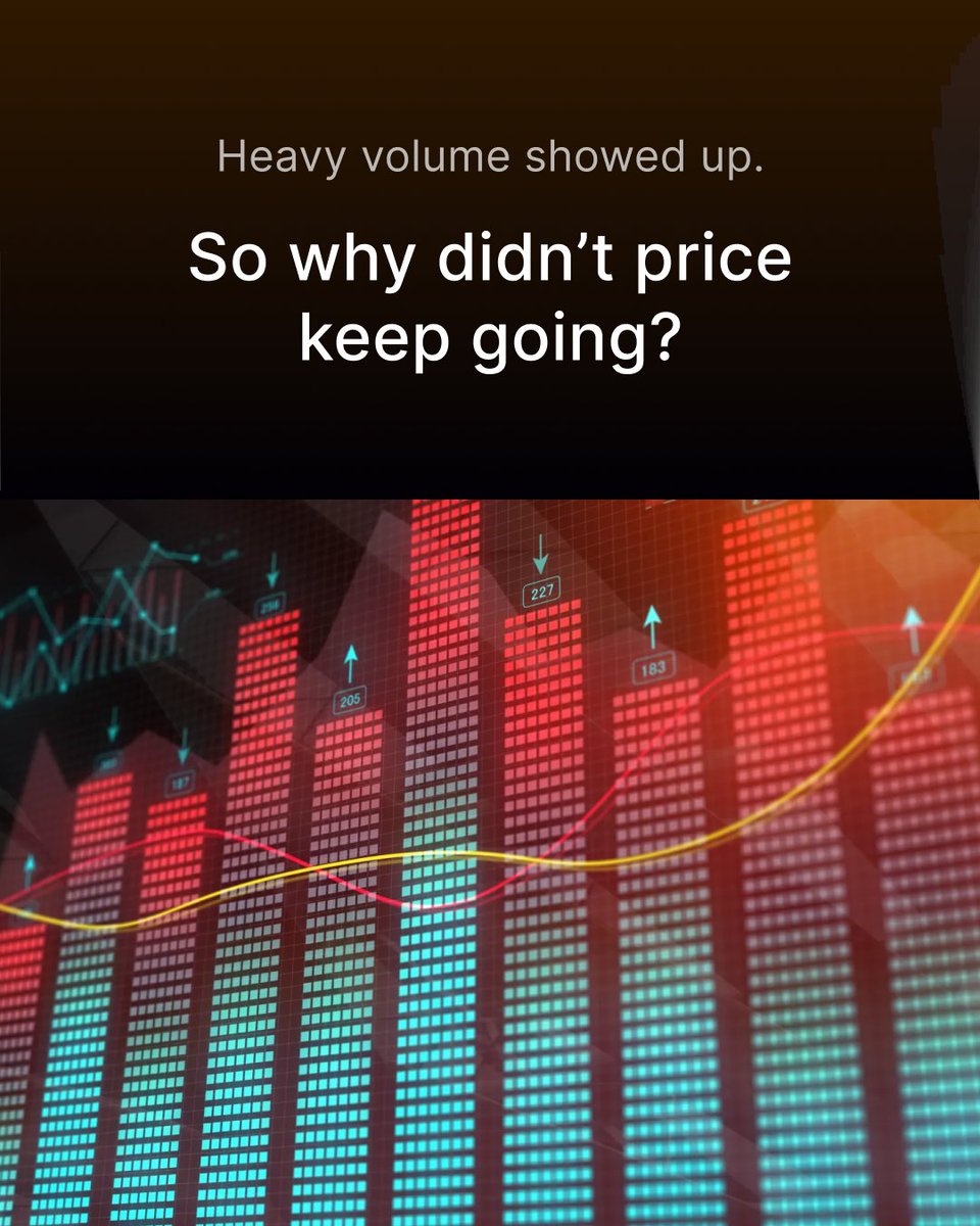
📊 Market read: heavy volume can look like confirmation…
until price refuses to continue
That’s the part traders often miss in real time. A volume spike shows participation, but it doesn’t automatically mean one side is in control
#blog #blogarticle
1
6
693
May 21
Market read: price just traded through prior value with almost no reaction ⚠️
No stall.
No clean rejection.
No obvious defense.
That’s usually worth paying attention to because the lack of response can be the signal
#blog #blogarticle

1
3
740
May 21
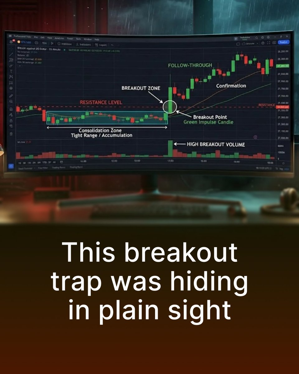
The “clean breakout” is getting harder to trust ⚠️
Not because breakouts stopped working
In more automated markets, obvious levels can act as trigger points for liquidity sweeps, stop runs, and rapid shifts in order flow
#blog #blogarticle
1
3
527
May 20
A reversal doesn’t always start with price.
Sometimes it starts with positioning. 📊
When large speculators are heavily leaning one way, the chart can still look strong, but the market underneath may already be getting crowded.
#blog #blogarticle

1
4
405
May 19
Retail traders don’t need to be faster than the machines.
They need to be better at deciding when the market is still worth participating in.
Hard choice for traders:
Would you rather enter earlier with less confirmation or wait for confirmation and risk being late?
Read the full article:
🔗 f.mtr.cool/amfzaqplny
#blog #blogarticle
3
244