"PushPull": It's a trans lesbian sex zine. Some of the characters are demons. There's quite a lot of pages of sketches that I wish were more fleshed out.

31


Jun 10
Niemcy już w 1971 zmodernizowały wagony i wstawiły kabiny żeby jeździł jak PushPull. Czemu w Polsce się nie dało?
direktzug.com/zuglexikon/int…
1
1
10

Jun 9
claudeくんがもはやgithubにpushpullまでしてくれる
ガードレールによって回答がいっさい信用できない部分もふくめてchatGPTの優位性ひとつもないな?
1
28

May 29
押し引き処理(PushPull)です。従来のアドバンシングガードの押し判定付きのヘルパーを出現させる方式ではなく、相手を直接移動させます。近い敵、敵全部、helperのみ、味方のみ、自分以外すべての指定ができます
2
96

What's wrong with you @SCRailwayIndia? Why are you neglecting the Kazipet-warangal route? We see a trend where existing trains like pushpull are cancelled in Warangal route & Most of the new trains are being introduced in Nalgonda-Guntur route? Why so much negligence on Warangal?
4
89

May 12
Better to start another train from Kazipet /wl durning hours .. as we have very few train ..after pushpull only bhagyanagar which runs late and take 3.55 hrs to reach secunderabad. If we had another train around 6:45 then it would be good for both people of WL/KZJ
1
4
139

May 10
Please advice this to Indian Railways which has paucity of WAP7s & is hauling trains with either WAG9s or Diesel Locos in fully electrified sections and using EoG (Generators) to power electricity supply to LHB coaches
Now they're using 2 WAP7/5 Locos in PushPull in Amrit Bharat

3
7
217

What is happening with the CR Rajdhani?
Yesterday it came to Mumbai in the afternoon with only one wap7 that too from TKD shed. No pushpull was used!!!
4
1,244
Push/Pull Workouts Can Take Your Training Up a Notch 💪 Discover how this method can help you build strength, balance, and results! Ready to level up? Check out the full guide: barbend.com/push-pull-workou…
#PushPull #StrengthTraining #WorkoutTips #Fitness #Exercise #Wellness #GetFit #NoExcuses #FitFam #Motivation #FitnessJourney #BodyweightWorkout #HomeWorkout #Training #Active #Healthylifestyle #FitnessHacks101

1
3
313

Apr 28
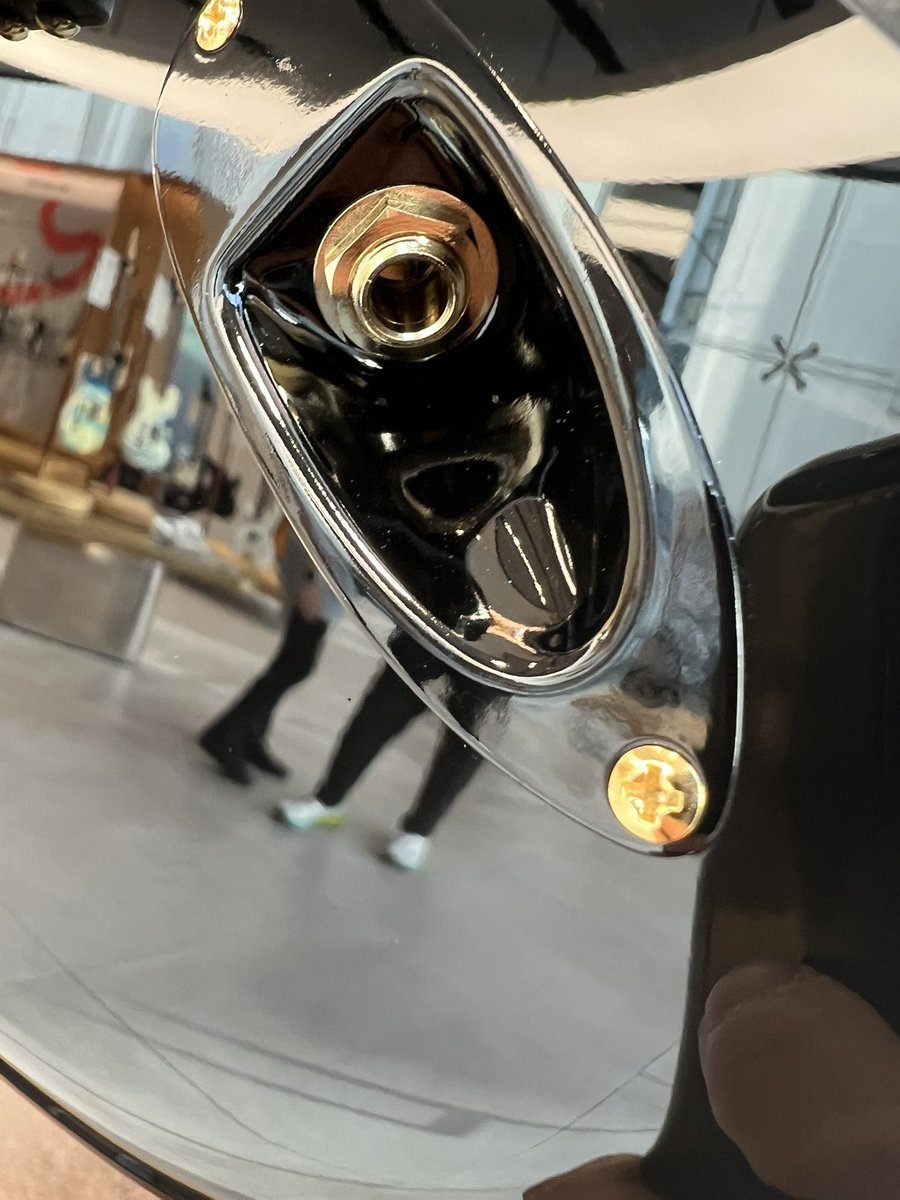
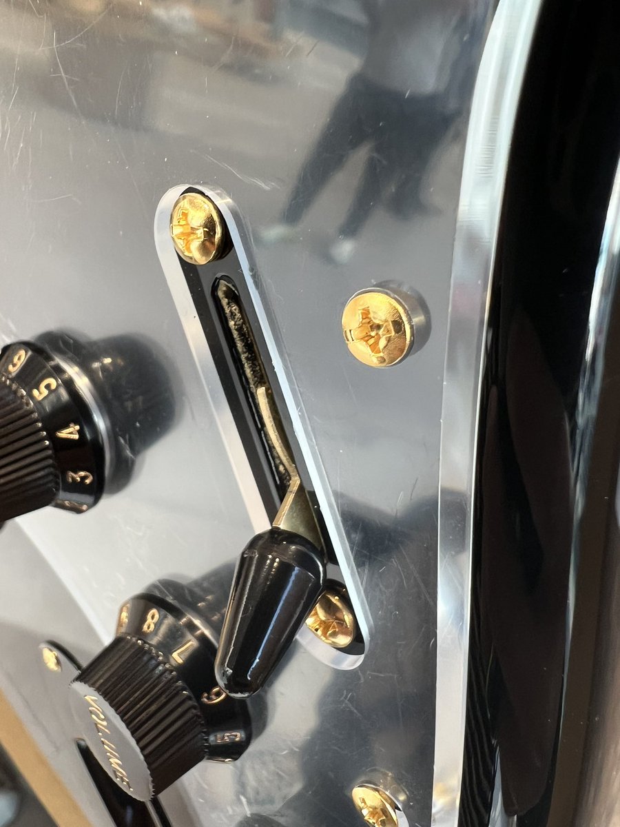
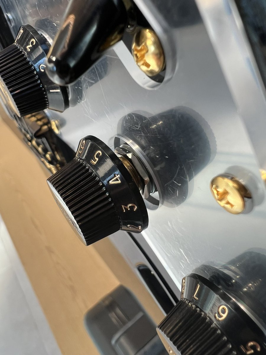
これはfishmanの音色切り替えです!pushpull Switchわりとギターで使います!

@CHLionRagbaby 細かいところまで見れてよかったです!
ジャックもピックアップも金で統一されてて、こだわりが凄いなぁと!
ボリュームがスイッチ?になってるのもこだわりですか?
2
1
25
2,483

There's no way to escape pushpull reddit search other than not saying anything out of pocket in the first place, that place captures everything.
3
105


Mar 31
@Offtejasvisurya @Tejasvi_Surya @BJP4Karnataka Sirs kindly request you to pls start Mumbai Bengaluru PushPull AC exp on lines of rajdhani exp wid 16 hrs run time, limited halts. This is need of hour for ever neglectd Mumbai-Bengaluru rail corridor.@AshwiniVaishnaw @RailMinIndia
Mar 31

CSMT NZM Rajdhani Express (20-21 Coaches ) takes 18 hours to cover journey still it is popular among passengers
Why @Central_Railway , @SW don't run Such Push Pull AC Express bw Mumbai & Bengaluru.
@AshwiniVaishnaw

1
7
9
175

Mar 28
Routines and Guide for Building Muscle with Push-Pull Workouts healthline.com/nutrition/pus…
#FitnessHacks #MuscleBuilding #PushPull #StrengthTraining #WorkoutRoutine #FitnessTips #GetStronger #GymMotivation #WellnessJourney #HealthyHabits

1
1
338
Mar 23
Push/Pull Workouts Can Take Your Training Up a Notch 💪 Discover how this training split can boost your results! Read more: barbend.com/push-pull-workou…
#FitnessTips #WorkoutMotivation #StrengthTraining #PushPull #GymLife #FitnessJourney #Wellness #HealthyHabits #GetStronger #FitnessHacks101

2
425
Mar 21
This Push-Pull Resistance Band Workout Will Pump Your Upper Body 💪 Check out this effective routine to build strength and boost your fitness! 👉 ow.ly/Kch250YqApF
#FitnessHacks #ResistanceBands #UpperBodyWorkout #StrengthTraining #HomeWorkout #FitnessTips #WorkoutMotivation #GetStronger #PushPull #WellnessJourney

1
2
342

🔌Push. Lock. Done.
Upgrade your M12 connection experience with M12 Pronto by Amphenol LTW.
⚡ Faster installation
🔄 Seamless compatibility
💧 IP67 / IP68 protection
Learn more👇
youtube.com/watch?v=OCGOYVrb…
#Amphenol #ALTW #M12 #PushPull

2
112

Mar 16
I FORMALLY CHALLENGE THEE (@i2cjak) TO AN EE DESIGN CHALLENGE
(rendered in the TONE of an i2cjak wannabEE ARTICLE):
ANON… I HAVE A PROPOSAL.
a DESIGN CHALLENGE.
a TEST of SKILL.
a TEST of GRIT.
a TEST of whether you are a REAL ELECTRONICS ENGINEER or merely someone who COPY PASTAS application notes written by some TI intern named KYLE.
let me set the stage...
imagine a world where you need to convert 12v into 48v.
this is not a crazy number. this is just BOOSTING a voltage.
people have been doing this since before your GREAT GREAT grandparents knew what a transistor was (i2cjack just turned 14).
and yet…
what does an i2cjak do?
he goes to MOUSER (he was banned from digikey) and he types: "BOOST CONVERTER"
he grabs some $6.37 switching regulator IC that hardly has any stock, has 87 internal op amps, slope compensation, cmc, undervoltage lockout, soft start, thermal shutdown, brownout detect, a coffee maker, and a SMALL GOBLIN that tunes the loop compensation FOR HIM.
he then looks himself in the mirror and calls himself A HARDTECH ENGINEER.
he slaps down one inductor, a diode, some caps, and a prayer.
NO. not today anon.
THE CHALLENGE:
• design a 12v to 48v dc/dc converter
• highest efficiency @ 10A/480W wins
but there are RULES.
and they are CRUEL.
RULES:
• NO SWITCHING REGULATOR ICS
• no boost controllers
• no flyback controllers
• no "smart power stages"
• no little black boxes that say "PWM controller" on the datasheet
• if the datasheet contains the phrase "switching regulator" you are DISQUALIFIED
ALLOWED COMPONENTS:
• a microcontroller
• gate drivers (maybe)
• power transistors
• diodes
• discrete analog
• discrete logic
• passives
THE CONTROL LOOP:
• must be written entirely BY YOU
• no OTS analog compensation network that MAGICALLY stabilizes everything
YOU WILL:
• fab the board at a fab house of your choice
• solder it YOURSELF
• measure voltages YOURSELF
• measure currents YOURSELF
• perform step response YOURSELF
• perform load sweeps YOURSELF
• measure EFFICIENCY YOURSELF
• you know, REAL EE SHIT YOURSELF
like the founding fvcking fathers intended.
ANY TOPOLOGY IS FAIR GAME:
• boost
• flyback
• forward
• pushpull
• interleaved
• some cursed topology you invented at 3am
i do not care. but it must convert 12v to 48v. and it must fvck.
SCORING:
highest measured efficiency @ 10A wins (adjusted for BOM cost).
WHY THIS IS FUN:
because suddenly all the stuff those nice little regulator ICs do for you becomes YOUR PROBLEM. you must engineer. ELECTRICALLY.
things like:
• current limiting
• duty cycle saturation
• loop stability
• slope compensation
• dead time
• gate drive timing
• startup behavior
• transient response
EXPECTED OUTCOMES:
• REAL EE is harder than it looks, i might fail. you might fail. BUT WE ALL LEARN.
• writing a control loop from scratch is CURSED.
• switch node ringing is DEMONIC.
and guess what i2cjak, the inductor you'll pick will be WRONG!!! your efficiency will mysteriously drop by 15% because physics HATES YOU!!!
but, you are a MANIAC. and you will eventually produce something BEAUTIFUL even IF it is covered in your BLOOD, SWEAT, AND TEARS.
so anon.
do you ACCEPT the challenge?
or will you retreat back to your TPS5430 application notes like a frightened little B*TCH?
MAY THE SUPREME WIZARD OF ELECTRONS WIN!!!

62
21
481
52,293