
Joined June 2007
- Tweets 8,508
- Following 7,502
- Followers 883
- Likes 141,847
143 Photos and videos


philtran.eth 🎉🦍 | ETHGas ⛽ retweeted

May 26
After reading Huawei's paper, my takeaway:
Huawei's innovation is fundamentally about using high design complexity high manufacturing cost bleeding-edge thermal solutions, to partially close the process gap
Huawei's Tau Scaling Law marketing is just another way of saying More than Moore: the generalized Moore's Law that everyone already knows.
What I'm actually interested in is whether Huawei's claimed density improvement brings real power efficiency gains. The 41% power efficiency number on their PPT , how is it actually achieved?
---------------------
1. Is Huawei's "equivalent density improvement" from chip stacking real or misleading? Is it a process breakthrough? Are there tangible benefits?
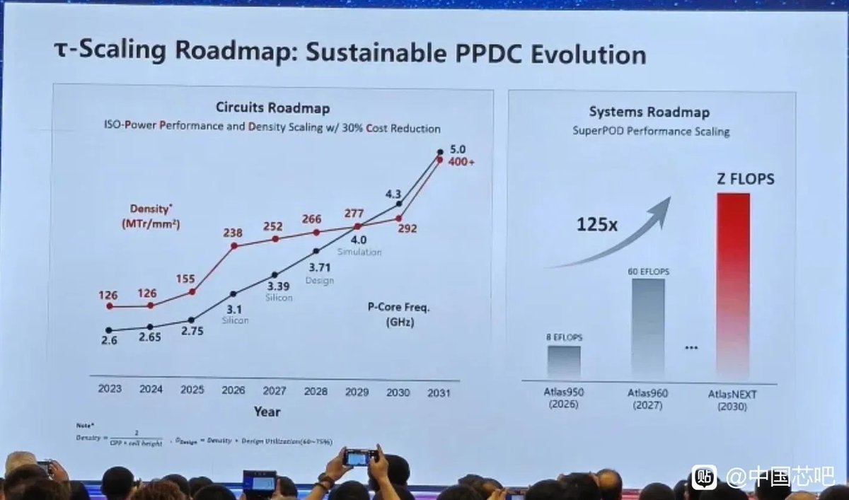
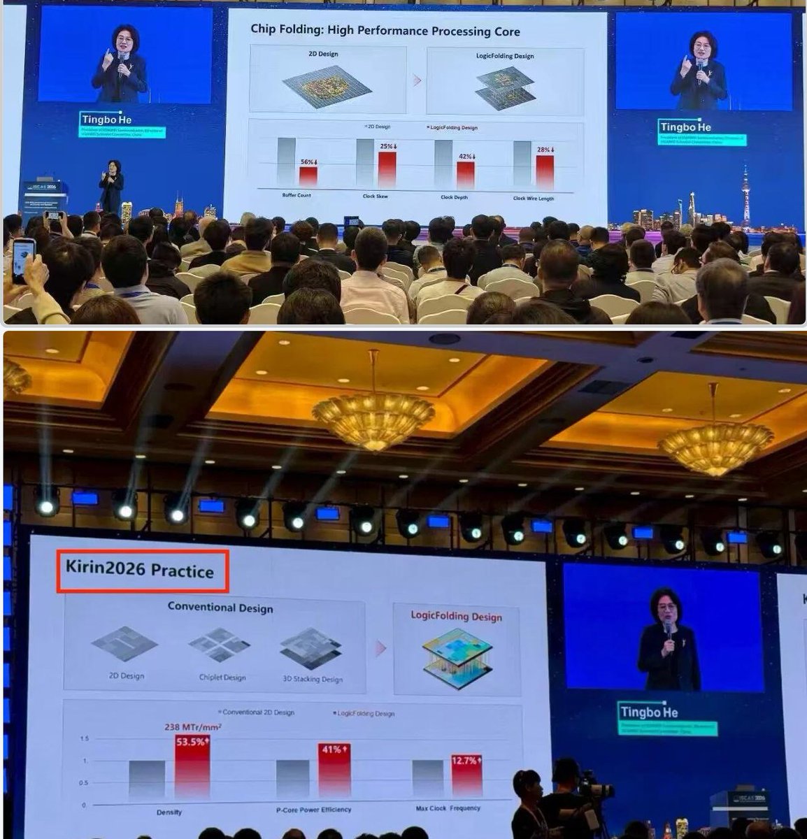
The source of the equivalent density improvement is two pieces of silicon bonded together using hybrid bonding technology. In theory, the projected footprint could be cut in half. But the first generation is not full-chip double-layer folding — it selectively folds critical logic paths. Only about 53% of the chip area is actually folded (density goes from 155 to 238 MTr/mm²). In subsequent generations, folding coverage will gradually increase, approaching full-chip folding by 2030 (density 155→292).
The 2026 first-generation equivalent density jumps from 155 MTr/mm² in 2025 to 238 MTr/mm² in 2026. Clock frequency also improves by 12.7%, and power efficiency improves by 41%. On the surface, this looks no different from a process node advancement. But there's one critical difference: Huawei never once mentions leakage power. As long as the process node doesn't change, I_off, gate leakage, and junction leakage won't improve from 3D stacking alone.
The density discontinuity from 2030 to 2031 most likely comes from moving from 2-layer to 3-layer stacking, just as the 2025-to-2026 density and clock frequency discontinuity comes from going from single-layer to 2-layer folding.
So clearly, the "1.4nm equivalent by 2031" claim has no connection to an actual process node breakthrough.
What it really is: using high design complexity high cost bleeding-edge thermal management early deployment of advanced packaging to partially compensate for the process gap.
---------------------
So is this seemingly inflated equivalent density improvement actually useful? What are the real benefits?
Yes, there are real benefits. The topological folding means that signal paths that previously ran several millimeters horizontally now become tens of micrometers vertically. This shortens super buffers and buses, reduces clock tree depth (clock depth -42%, clock wire -28%), and improves clock skew (-25%). These translate into genuine dynamic power savings. The shortening of critical paths also makes clock frequency increases easier to achieve.
So the performance improvement shown on the PPT roadmap — the 12.7% gain from 2025 to 2026 — is almost entirely from clock frequency increase (12.7%).
The benefits are fundamentally from topology-driven circuit design improvements.
---------------------
Since there's no actual process improvement, what are the trade-off costs of Huawei's chip stacking?
Three costs: thermal management gets harder, design complexity goes up, and manufacturing cost increases.
The biggest cost is the simultaneous increase in thermal density. In theory, logic-on-logic stacking means the hottest CPU execution areas have their power density effectively doubled. But factoring in the 41% power efficiency improvement, the actual power density is only about 40-50% higher than the non-stacked design. That's why the first generation can only fold the most critical portions — roughly 53% of the chip area.
This forces thermal technology to advance ahead of schedule. Huawei is deploying millimeter-scale MEMS fans as micro-cooling solutions.
The second cost is design complexity. Which logic blocks can be folded? Once folded, the entire flow from front-end to back-end design has to be reworked.
No existing EDA tools support 3D topology. The paper itself admits that full-scale LogicFolding requires an entirely new 3D-native EDA toolchain that treats multi-layer stacked dies as a single continuous design entity. Which logic can be folded, how to perform inter-die timing closure, and physical design (PD) are all significant challenges.
Manufacturing cost also goes up significantly, forced into early deployment of advanced packaging. 1.5-2μm hybrid bonding combined with logic-on-logic is extremely challenging and substantially more expensive. Previously, one wafer layer required one lithography pass. Now two wafer layers are lithographed separately and then bonded, with hybrid bonding overlay control (the paper requires <0.5μm), TSVs, KOZ keep-out zones, redundancy and repair, and multiplicative yield losses. Per-chip manufacturing and testing costs increase significantly.
---------------------
2. What is Tau Scaling actually scaling? Is this a one-time design topology dividend? What's the potential? Where does continued improvement come from?
The core claim of τ Scaling is: replace geometric linewidth with the time constant τ as the full-stack optimization target, compressing characteristic delay across four levels — device, circuit, chip, and system.
The formula itself contains no new physics. "Focus on the bottleneck delay" is what every architect already does. The entire industry knows that interconnect RC is the delay bottleneck. TSMC has been using low-k dielectrics, semi-damascene, and other techniques to reduce RC with every process generation. Packaging a universally known optimization direction as a "law" is clearly a marketing move. It's essentially just another way of saying More than Moore — the generalized Moore's Law.
Setting the marketing aside, Huawei's claimed RC delay improvement is fundamentally about topology distances shrinking after chip stacking, which reduces the effective RC along those paths — not the RC process constants themselves.
As for what "scaling" means here, it refers to a sustainable roadmap of continued improvement. The path is: increasing the number of stacked layers across the full chip, from 2-layer stacking in 2025-2030, to 3-layer stacking starting around 2031, and potentially 4-layer stacking further out.
The first-generation folding technology isn't even full-chip double-layer folding. It selectively folds critical logic, with only about 53% of the chip area folded (density 155→238). In subsequent generations, folding coverage will gradually increase, approaching full-chip folding by 2030 (density 155→292). The reason the 2031 roadmap shows a density discontinuity is precisely because that's the transition point from 2-layer to 3-layer folding.
But note that the marginal returns of this scaling approach diminish with each layer. Folding from 1 to 2 layers yields up to 100% density gain. Going from 2 to 3 layers yields only 50%. If they go from 3 to 4 layers around 2035, the yield is only 33%.
And as the number of stacked layers increases, all three challenges mentioned above — thermal, design complexity, and cost — get progressively worse.
---------------------
3. Is Huawei's chip stacking the same hybrid bonding technology that TSMC/AMD already have? Is it cache-on-logic, cache-on-cache, or logic-on-logic? How is the thermal problem of logic-on-logic solved?
Yes, it uses existing technology. But it's also true that Huawei has pushed certain metrics to industry-leading levels. 3D stacking itself is not new, but TSMC's production hybrid bonding is still at 6μm pitch. Huawei's paper states that Kirin 2026 uses a 1.5μm hybrid bonding pitch.
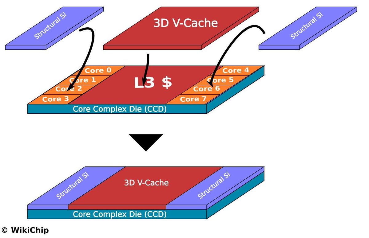
When I first saw the stacking news, my initial reaction was to suspect it was similar to AMD's 3D V-Cache, which primarily stacks SRAM cache on top of the existing L3 cache area and typically avoids stacking directly above the hottest CPU execution logic — precisely to avoid thermal issues. SRAM has different power density and thermal characteristics than high-activity logic. If you stack the hottest logic-on-logic, thermal management becomes extremely difficult.
But after seeing more data — clock buffer -56%, clock depth -42%, clock wire -28% — these numbers are only possible if the core's internal clock distribution has been restructured. Pure SRAM stacking wouldn't touch the core's internal clock tree. Furthermore, cache-on-cache alone would likely not require a dedicated MEMS micro-fan for additional cooling. The evidence overwhelmingly points to a logic-on-logic approach.
The elegant aspect of Huawei's approach is that logic-on-logic folding doesn't actually double the thermal density, because the topological benefits reduce power consumption by about 30%. This means the thermal density only increases by about 40-50%.
And the first generation doesn't fully stack 100% of the hottest execution logic. The paper explicitly says it's "selectively applied along key critical paths." Only about 53% of selected critical paths are stacked, and the granularity may not even be that fine — it could be IP-block-on-IP-block stacking. In that case, the actual thermal density increase might stay within 20%.
But as this path continues forward, bleeding-edge thermal solutions become inevitable. Right now it's millimeter-scale MEMS fans placed directly against the processor for high thermal conductivity. Like Huawei's phones in general, the thermal engineering is aggressive and leads the industry.
Going forward, they may need to bring HBM7/8's microchannel cooling technology forward in time. After all, HBM7/8 will feature 24 layer stacking, and Huawei may well need to deploy next-generation thermal solutions ahead of schedule.
---------------------
4. From an architecture perspective, the most important question: How is Huawei's 41% power efficiency improvement actually achieved? Why didn't AMD's 3D V-Cache produce a similar improvement?
First, let's pin down what 41% means. The paper only says "SoC performance-core power efficiency improved by 41%," without specifying the benchmark, voltage/frequency operating point, temperature conditions, or power boundary. But there's a key clue on the PPT roadmap: the ISO-Power Performance numbers are 2.75 for 2025 and 3.1 for 2026 — a 12.7% improvement.
This matches the clock frequency increase of 12.7% exactly. This can be interpreted as: the performance improvement at constant power is 12.7%, and it's almost entirely from clock frequency.
My hypothesis for how the power efficiency improvement works: LogicFolding shortens the critical path → at a fixed Vdd, Fmax increases from 2.75GHz to 3.1GHz → this means at the original 2.75GHz, there's approximately 12.7% timing headroom → this headroom can be traded for lower Vdd in iso-performance mode.
Additional power efficiency gains likely come from reduced cache hit latency after circuit folding. From industry experience, a 10% reduction in L2/L3 cache hit latency typically translates to at least a 5% overall CPU performance improvement.
The PPT shows SRAM latency reduced by 30%, and some portion of that likely translates into lower cache hit latency.
AMD's 3D V-Cache didn't produce a comparable improvement mainly because AMD's underlying logic die wasn't redesigned. The 3D cache latency actually increased rather than decreased — it only added cache capacity. The benefit of increased capacity is less dramatic than the benefit of reduced latency.
On the other hand, the reduction in clock skew and shortening of critical paths improve circuit timing, meaning Huawei can use a lower Vdd (I estimate possibly 7-8% lower). Combined with the RC reduction from shorter paths (considering clock buffer -56%, wire -28%, SRAM pJ/bit -24%, a C_eff reduction of 10-15% seems reasonable), plus the overall shrinking of the clock tree, it's entirely possible to achieve a 30% power reduction at iso-performance on certain voltage/frequency operating points. And a 30% power reduction translates to exactly 41% power efficiency improvement.
For comparison, Apple and Qualcomm typically see iso-power single-core performance improvements of 10-20% per generation, and iso-performance power reductions of 30-40%. This is determined by the shape of the V/F curve. So empirically, the numbers check out.
The power efficiency improvement, based on the available data, can be derived from topology changes and appears to be plausible — it may genuinely have little to do with the process node.
---------------------
5. Is this technology path replicable? Will others follow?
In the short term, no one will replicate this at scale, because the risk-reward ratio doesn't justify it. In the long term, everyone is heading in this direction — just under different names.
Huawei's fundamental motivation for LogicFolding is the sanctions. With the process node capped at 7nm, the only option is to compensate through packaging and design. Huawei has paid a significant price for this: thermal engineering costs, design complexity, and higher manufacturing costs (including yield). This is a path born of necessity, not natural choice.
Other players who can access TSMC can achieve normal economic iteration without taking on the risk of prematurely pushing thermal technology and design complexity forward.
In the long term, Intel's Foveros, TSMC's SoIC, and AMD's MI300 3D stacking are all heading in the same direction. If the economics of chasing the most advanced nodes continue to deteriorate, then "fix a mature node 3D topology optimization" will become increasingly attractive.
On the thermal front, MEMS micro-fans and microchannels are likely to become mainstream for future HBM cooling as well.
---------------------
In summary, Huawei's innovation here deserves genuine respect. Under sanctions, they've used extreme design complexity and cost to boldly redesign on a locked process node, extracting a significant one-time topology dividend — though it has a ceiling. The marginal returns diminish with each additional layer (1→2, 2→3, 3→4 layers yield progressively smaller percentage gains). Leakage remains unsolved. Thermal management gets harder. The 3D EDA toolchain is an entirely new challenge.
Tau Scaling is not a path that sustains exponential growth for a decade. Each step up the staircase is harder to climb, and each step is shorter than the last. If Huawei wants to continue closing the gap, they'll need to find other routes beyond this one.


May 26

华为τ scaling定律营销策略,无非是more than moore的广义摩尔定律的另一种说法而已
作为芯片架构师,我更感兴趣的,还是芯片密度提升,ppt上41%能耗提升和12.7%性能提升,到底是怎么实现的
看完了论文,感觉华为这次创新,本质上是用设计复杂度高 高制造成本 超前散热,一定程度弥补了工艺差距
-----------------
1. 华为芯片堆叠带来的等效密度提升,是虚假宣传还是真的,是不是工艺突破?有没有实打实的好处?
等效密度提升的来源,是两片芯片用hybrid bonding技术绑在一起,投影面积理论上能减小一半,但第一代不是全芯片双层折叠,而是选择性折叠关键logic,所以只有大概53%的芯片面积实现了折叠(密度155->238),等到后面几代折叠面积会逐渐增大,到2030年接近全折叠(密度155->292)
这2026第一代等效密度从 2025 年 155 MTr/mm² 跳到 2026 年 238 MTr/mm²,时钟频率也提升了12.7%,功耗比提升41%,表面上看似乎和工艺突破没有什么区别,但有一点重要区别就是leakage power华为从头到尾没有提,只要工艺节点不变,gate leakage、junction leakage 不会因为 3D stacking 自动改善
2030年到2031年的等效密度突变,大概率是来自于2层堆叠到3层堆叠,正如2025到2026年的等效密度突变,时钟频率突变,来自单层到2层折叠
所以从leakage没提这个事来看,这个2031年等效1.4nm,和工艺节点上的突破没有联系。
本质上是用设计复杂度高 高成本 超前散热 超前部署advanced packaging,一定程度弥补了工艺差距
-----------
那么这样看起来虚假的等效密度提升,有用处吗?好处在哪里?
有的,设计上topology折叠,原来要跑几毫米的水平走线,折叠后变成了几十微米。降低了super buffer/bus的长度,降低了clock tree的深度(clock depth -42%、clock wire -28%),clock skew也带来了改良(-25%),这对动态功耗的改善是实实在在的。部分critical path的缩短,也让时钟频率的上升更容易
所以ppt roadmap上performance的提升,从2025年到2026年上升了12.7%,大部分都是来自于时钟频率的上升(12.7%)
所以好处基本上是topology拆分电路逻辑设计上带来的提升
既然没有实质上的工艺提升,华为芯片堆叠带来等效密度提升的trade off代价在哪里?
三个代价:散热超前发展,设计复杂度高,制造成本变高
最大的代价就是热密度的同步上升,理论上logic on logic都是CPU execution发热最严重的区域,这部分折叠起来相当于功耗密度直接翻倍,但算上41% power efficiency改善,功耗密度仍只比非堆叠方案高40%左右。所以第一代只能对最关键的部分做折叠,大概只占全芯片面积的53%。
所以散热技术也被逼的超前发展,直接上毫米级的MEMS风扇,做micro-cooling fan。
另外的代价就是设计复杂度的变高,critical path的折叠,哪个部分的logic能折叠,折叠之后又会带来从前端到后端的巨大变化要推翻重来
现有的所有EDA工具也不可能支持3D topology,论文自己也承认,full-scale LogicFolding需要全新的3D-native EDA toolchain,把多层stacked dies当作单一连续设计实体处理。哪些logic能折叠、折叠后的inter-die timing closure怎么做,Physical Design(PD)也是难点
制造成本也会更高,被迫超前部署advanced packaging封装,1.5~2um的hybrid bonding logic on logic都是很有挑战需要显著更高的成本
以前一层wafer做一次光刻;现在两层wafer分别做光刻再bonding,加上hybrid bonding的overlay控制(论文要求<0.5μm)、TSV、KOZ keep-out zone、冗余修复、良率乘法损失,每颗芯片的制造成本和测试成本都要显著上升
--------------------------
2. Tau scaling这个说法,scaling的到底是什么,这个scaling技术路线是不是一次性的design topology红利?潜力如何?持续进步的空间在哪里?
τ Scaling的核心主张是:用时间常数τ替代几何线宽作为全栈优化目标,在器件、电路、芯片、系统四个层级分别压缩特征延迟
公式本身没有任何新物理。"关注瓶颈延迟"是所有架构师都在做的事情。整个行业都知道互联RC是延迟瓶颈,TSMC每一代工艺都在用low-k dielectrics/semi-damascene等手段降RC。把一个众所周知的优化方向包装成"定律"是显然的营销宣传手段,本质是More than Moore的广义摩尔定律的另一种说法
抛开marketing,华为目前所谓RC delay的改善,本质上是芯片堆叠之后,topology距离缩短,让匹配的effective RC都变小,不是RC工艺常数
至于scaling的意思,是能持续发展的一条roadmap。这里的持续改善路径指的是,全芯片堆叠的层数越来越多,从25~30年的2层堆叠,到31年开始的3层堆叠,以后甚至会考虑4层堆叠
第一代折叠技术甚至不是全芯片双层折叠,而是选择性折叠关键logic,所以只有大概53%的芯片面积实现了折叠(密度155->238),等到后面几代折叠面积会逐渐增大,到2030年接近全折叠(密度155->292)。2031年的roadmap之所以会出现一个阶跃,就是因为那是从2层折叠到3层折叠的时间点。
但需要注意的是,这个scaling方法的边际效应是逐渐缩小的,折叠成双层的收益是100%,2->3层的收益就只有50%,如果2035年再从3->4层堆叠,收益就只有33%了
另外随着堆叠层数变高,上面说到的三个挑战,散热,设计复杂度,成本,都是越来越大
---------------------
3. 华为的芯片堆叠,是不是TSMC/AMD已经有的hybrid bonding技术?华为做到的是cache on logic,cache on cache,还是logic on logic,logic on logic最大的散热问题是怎么解决的?
是已经有的技术没错,但同时也是把现有技术指标做到了领先也是真的,3D堆叠本身不是新技术,TSMC的hybrid bonding量产还是6um,华为论文给出Kirin 2026的hybrid bonding pitch是1.5μm
我在刚刚看到华为的堆叠消息之后,第一反应也是怀疑和AMD的3D V cache类似,它主要把 SRAM cache 叠在 已经有的L3 cache 区域上,通常会避免直接堆在最热的 CPU execution logic 上,就是避免散热问题,毕竟SRAM 的功耗密度和热点特性与high-activity logic 不一样,如果最热的logic on logic堆叠,散热恐怕会碰到困难
但看了更多数据之后,clock buffer -56%、clock depth -42%、clock wire -28%,这些只有在core内部的clock distribution被重构时才可能发生。纯SRAM stacking不会碰core内部的clock tree。另外如果只是cache on cache,大概率是不需要单独MEMS微型风扇额外散热的,证据普遍都指向logic on logic方式
华为这个技术的精妙之处在于,logic on logic 折叠之后热密度并没有翻倍,而是因为topology的好处,能耗下降了30%,这样热密度只上升了40~50%
而第一代没有完全把整个最热的execution logic 100%堆叠起来,论文也明确说selectively applied along key critical paths,只是大概53%有选择性关键路径会堆叠起来,可能颗粒度都没有那么好,只是IP堆叠在IP上,那么热密度上升也许能维持在20%以内
但这条道路继续前行,超前发展的散热就成了必然,现在是MEMS微型毫米级的主动散热风扇,紧贴处理器传导效率高,和华为手机一样,散热堆料特别足,而且技术领先同行。
以后怕是要把HBM7/8的微流道散热技术提前用起来了,毕竟HBM7/8要上24 层堆叠,华为很可能要在提前用上下个世代的散热技术了
-------------------------
4. 从架构角度来说,最重要的问题,华为41%的power efficiency(能耗比)提升,到底是怎么实现的?为什么AMD的3D V cache没有这么大的提升?
首先确定41%的定义。论文只说"SoC performance-core power efficiency improved by 41%",没有给出benchmark名称、Voltage/Freq点、温度条件、功耗边界。但PPT roadmap上有一个关键线索:ISO-Power Performance的数字,2025年是2.75,2026年是3.1,提升12.7%
这个时钟频率提升12.7%完全一致,可以理解为,同功耗的性能提升是12.7%,绝大部分是时钟频率提升带来的
至于能耗比上优化的猜测是,LogicFolding缩短critical path → 在固定Vdd下Fmax从2.75GHz提升到3.1GHz → 这意味着在原来的2.75GHz频率下,有了约12.7%的timing headroom → 这个空间在iso-performance模式下可以换成更低的Vdd
另外的能耗比的提升,可能也来自于电路折叠之后,cache hit latency的下降。从业界经验来看,一般L2/L3 cache hit latency下降10%,CPU整体性能会有至少5%的提升
ppt里显示SRAM latency下降30%,估计会有一部分转化为cache hit latency的下降
AMD的3D V cache没有这么大的提升,主要是因为AMD的底层logic die并没有重新设计,3D cache的延迟latency不仅没有减小反而加大,只是增加了cache大小,收益不如latency下降那么明显。
另一方面,clock skew的下降,critical路径变短,造成电路timing变好,意味着华为可以使用更低的vdd(猜测甚至能低7~8%),以及路径缩短所带来的RC的下降(考虑到clock buffer -56%、wire -28%、SRAM pJ/bit -24%这些数字,比如C_eff下降10~15%合理),再加上clock tree的整体缩短和下降,确实是有可能在部分Voltage/Freq点做到同性能下,做到30%的功耗下降的,而30%的功耗下降换算过来就是41%的power efficiency
对比苹果和高通,每一代手机芯片在iso-power下单核性能一般提升10-20%,iso-performance下功耗一般降30-40%,这是V/F曲线的特性决定的,所以从经验上来说,数字是对的上的。
所以这个power efficiency(能耗比)的提升,从现有的数字上来说可以从topology推导出来是合理的,可能真的和工艺节点没有太大关系
----------------------------
5. 这个技术路线有没有可复制性,其他家会不会效仿?
短期内不会大规模效仿,因为性价比和风险收益比来说不好。长期来看,这个方向所有人都在走,只是名字不一样
华为做LogicFolding的根本驱动力是制裁,工艺节点被卡在7nm,只能在封装,散热,和设计层面想办法弥补。华为也为此付出了不小的代价:散热成本,设计复杂度,以及制造成本更高(包括良率)。这是一个被逼出来的路线,不是一个自然选择
其他玩家在用TSMC就能做到正常的经济迭代,是没有必要冒着这个风险,去超前迭代散热技术和设计复杂度的
长期来看,Intel的Foveros、TSMC的SoIC、AMD的MI300的3D stacking都在朝同一个方向走。如果继续追最先进节点的经济性持续恶化,那么"固定一个成熟节点 3D topology optimization"的路线会越来越有吸引力
散热方面,MEMS微型风扇和微流道也会成为未来HBM散热的主流
-------------------
总结一下,华为这次的创新,绝对是值得尊重的,在制裁环境下,用极高的设计复杂度和成本,在一个被锁定的工艺节点上大胆重新设计,榨出了一次大的topology红利,虽然它有天花板。每多加一层的边际收益递减(堆叠1->2层, 2->3层, 3->4层,提升百分比变小),leakage无法解决,散热越来越难,3D EDA工具链更是全新的挑战。
但这个Tau scaling不是一条可以走十年的指数增长路径,每次爬完一个台阶,下一个台阶更难爬,而且台阶更矮收益更小,华为以后想缩小差距,还得再想想靠什么其他的路线


12
46
288
64,310
philtran.eth 🎉🦍 | ETHGas ⛽ retweeted

May 17
China: a 10-year-old casually gets a Mac Studio for “raising lobsters,” aka letting multiple AI agents work together like a tiny digital crew.
“The world of the future belongs to those who understand Tokens.”
Meet the AI-native children.
115
400
3,083
347,618
philtran.eth 🎉🦍 | ETHGas ⛽ retweeted

如何不说脏话的读出这些词语
12
79
598
114,626
philtran.eth 🎉🦍 | ETHGas ⛽ retweeted

SCOOP: Sens. Tillis and Alsobrooks have finalized a compromise on stablecoin yield. Punchbowl News has the text
- bans rewards that are “economically or functionally equivalent” to deposit interest
- balances *can* be used for rewards if companies clear the “equivalent” test

41
136
557
913,669
TEAMZSummitに @BTCCVentures が参加中!
2026.4.7–8
東京・八芳園(Happo-en)
📍会場2階 B-G7 #TEAMZSummit2026 #BTCCTEAMZ2026 #TEAMZ #Web3
4
5
83
philtran.eth 🎉🦍 | ETHGas ⛽ retweeted

Feb 26
A creature unlike any other.
A dreamer, a disruptor … a … DEGEN.
777 supply. Free mint.
Q1 2026
Enter the dream → dream.degen.tips
100,361
52,779
63,912
1,403,883
philtran.eth 🎉🦍 | ETHGas ⛽ retweeted

Feb 25
Crypto Explained…
467
4,496
25,833
1,534,281
philtran.eth 🎉🦍 | ETHGas ⛽ retweeted

Feb 24
He is the singer Jon Bon Jovi, this picture is not a montage, his personal fortune is $410 million, and he washes trays and dishes in his chain of restaurants ( Soul Kitchen in Newark, New Jersey ) created by him for the homeless, where they eat for free forever ! These are influencers 🌎
A true idol ❤️

784
7,080
36,051
1,608,973
philtran.eth 🎉🦍 | ETHGas ⛽ retweeted

Feb 23
Hello again! Here's our piece from Sunday about Twitter. Bye! youtube.com/watch?v=p7ZG_xWY…
654
6,126
22,501
1,908,225
philtran.eth 🎉🦍 | ETHGas ⛽ retweeted

Feb 19
Silver is a $4T asset with zero presence on-chain.
That changes now.
Position early: loyalty.stackrs.finance
794
1,025
2,568
105,804
philtran.eth 🎉🦍 | ETHGas ⛽ retweeted

Feb 17
.@JamesTalarico: For 50 years, the religious right convinced our fellow Christians that the most important issues were abortion and gay marriage—two issues that aren't mentioned in the Bible.
Jesus tells us exactly how we're going to be judged: by feeding the hungry, by healing the sick, and by welcoming the stranger.
Don’t tell me what you believe. Show me how you treat other people, and I’ll tell you what you believe. Jesus gave us two commandments: love God and love neighbor.
There was no exception to that second commandment regardless of race, gender, sexual orientation, immigration status, or religious affiliation.
2,979
7,758
38,605
3,330,861

Feb 11
Here at the networking dinner by @Pudgypenguins, @Virtuals_io, @openmind_agi, @canonical!
Always a great time meeting likeminded individuals.
Thank you @penguasia for organising
2
32

923 Clawdbot gateways are exposed right now with zero auth (they just connect to your IP and are in)
That means shell access, browser automation, API keys.
All wide open for someone to have full control of your device.
Had Clawdbot check my setup:
- Config shows bind: "loopback"
- External port test: connection refused
(Not exposed)
If you're running Clawdbot, check yours:
bind: "all" means you're on that list
Fix: change to bind: "loopback" and restart.
It takes 10 seconds.
RT for exposure
Jan 25

Clawdbot is awesome 🦞
But I just checked Shodan and there are exposed gateways on port 18789 with zero auth
That's shell access, browser automation, your API keys
Cloudflare Tunnel is free, there's no excuse
RT to save a ClawdBot from getting cooked
107
421
3,124
571,069

Most yield products swing from 3% one week to 18% the next depending on market conditions.
SHRED offers a stabilized 10-15% APY on USDC. Smoothed by design.
Simple UX. No lockups. Backed by real revenues.
Waitlist is open for 5 days only ⏳
Join now 👉 waitlist.shred.fi
1,006
4,969
5,968
249,494
philtran.eth 🎉🦍 | ETHGas ⛽ retweeted

15 Dec 2025
Fintech 3.0 begins here ❗️❗️❗️
BonkX is now backed by @bonk_inu.
A long-term alignment built on product, culture and scale.
We're building the lifestyle NeoBank for the on-chain generation where payments become lifestyle: real status, real perks and rewards that matter.
More utility. More access. More reasons to run with the BONK economy.
BonkX. Building what banks can't.
BONK your bank
5,885
3,254
3,893
114,153
philtran.eth 🎉🦍 | ETHGas ⛽ retweeted

Jan 19
Being early still matters.
If you care about self-custody and privacy, BlockVault is the place.
This is what being early actually means:
– Airdrop eligibility
– Early product access
– OG on-chain status
This isn’t for everyone.
It’s for the ones who show up early.
Join the waitlist 👉 blockvault.ai/

2,165
2,555
2,830
98,968

Veera | The Onchain Neobank 💜
Invest, earn, borrow, and spend from one wallet.
🔐 Non-custodial
🌍 187 countries
👥 2M users
💳 30K cards
💼 Backed by CMCC Global, Accomplice, Reflective Capital more
Join the rewards hub for the upcoming airdrop👇
hub.veerarewards.com
38,023
22,032
25,995
710,061
Jan 19
claimed the @basedappcom Press Pass
trying to max this progression bar 👀
jump in with my link ↓
waitlist.basedapp.com/?ref=0…
1
15