
AHEAD OF THE HERD ™ | See our full portfolio and all live entries/exits at whop.com/stocktalk/stocktalk
Joined August 2020
- Tweets 56,141
- Following 927
- Followers 395,934
- Likes 41,244
6,440 Photos and videos


Pinned Tweet

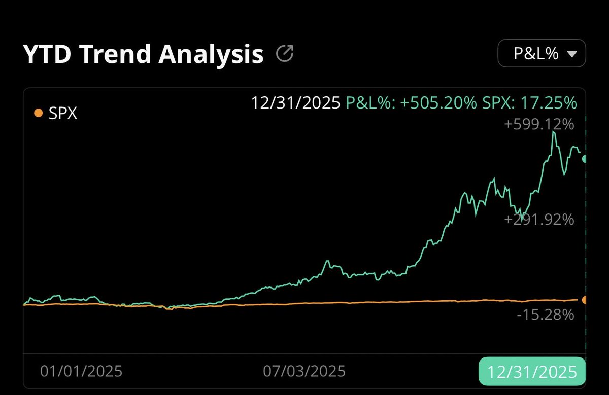
31 Dec 2025
FINAL 2025 FULL-YEAR PERFORMANCE
505.20% vs. 17.25% for S&P-500
Truly life-changing year for me. Full portfolio transparency the entire way shared with thousands of members.
No meme stocks and no 0DTE options. Just deep-research on themes & industries.
Proud & humbled.
164
76
1,557
521,278
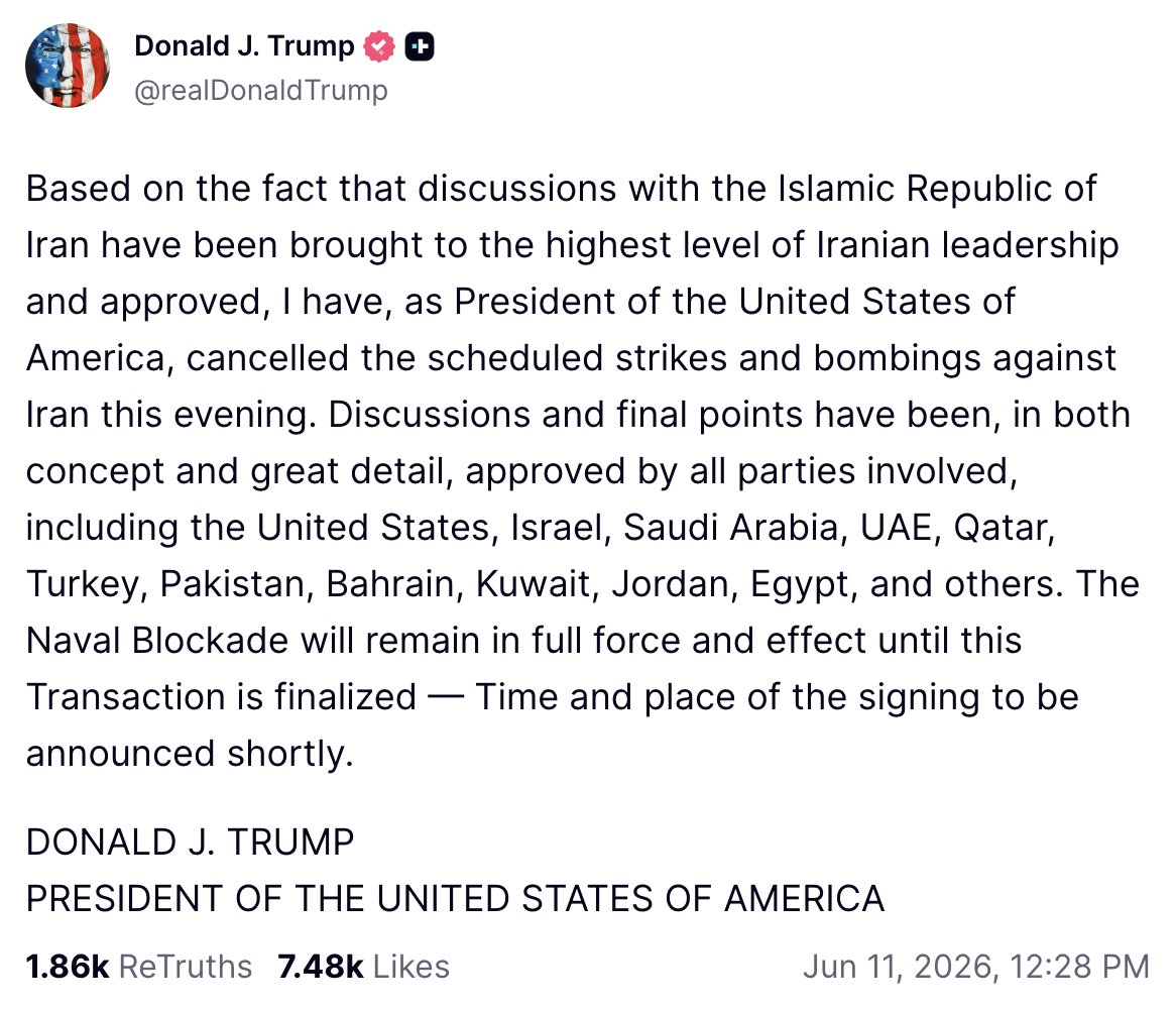
Jun 11
*IRAN AGREES TO OPEN STRAIT OF HORMUZ IN RETURN FOR SPACEX IPO ALLOCATION
378
545
10,385
1,206,195
Jun 12
Dear community noters please don’t ruin the fun, it’s obviously a joke, unless you’re sub 15 IQ…
14
2
342
32,700
Jun 12
What a wonderful journey with Nebius $NBIS
My aim is to find SMID caps that can become large-caps.
Nebius has done that for me.
It was a $5.6B mkt cap when I bought it a year ago at $23.92
Now, it’s a $56B mkt cap being added to the Nasdaq at $240 & my shares are up 900%
Jun 12

*NEBIUS TO JOIN NASDAQ-100 $NBIS
39
10
526
110,551
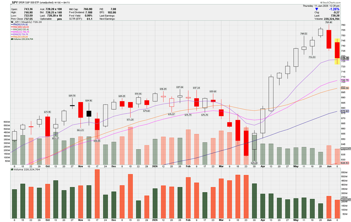
Jun 11
It was indeed a “do or die” spot
Jun 10
S&P-500 $SPY selling directly into the 9-week EMA today. Traditionally a "do or die" spot for uptrends. Thursday & Friday's action are critical to watch. Most important close to the week of the last few months.
20
2
161
34,703
Jun 11
*IRAN IRGC JOINT COMMAND: U.S. CONTRADICTORY BEHAVIOR IS MAIN CAUSE OF INSECURITY IN MIDDLE EAST... FIRE OF WAR WILL BECOME MORE WIDESPREAD... EITHER OIL & GAS EXPORTS ARE FOR EVERYONE, OR THEY WILL BE AVAILABLE FOR NO ONE...
47
11
137
24,247
Jun 11
S&P-500 $SPY is bouncing (albeit, very weakly) off this 9-week EMA level today, but the week isn't over. Tomorrow's action amidst the SpaceX IPO will be critical. Bulls must defend the weekly close. Watch this $726.78 spot into the end of tomorrow's session.
Jun 10
S&P-500 $SPY selling directly into the 9-week EMA today. Traditionally a "do or die" spot for uptrends. Thursday & Friday's action are critical to watch. Most important close to the week of the last few months.
15
7
164
36,767
Jun 11
A reminder for the young & risk-tolerant investors who trade & invest in market leaders, SMID caps, and speculative companies:
If you wish to outperform with high-beta on the way up, you will underperform with high-beta on the way down.
Live by the sword, die by the sword.
27
15
592
44,063
Jun 10
Be careful about marrying relative strength. It is true that when markets bounce back quickly, relative strength stocks often assert themselves as new leaders. However, when markets don't bounce back quickly, relative strength stocks are often just the last dominoes to fall.
25
23
441
39,429
Jun 10
S&P-500 $SPY selling directly into the 9-week EMA today. Traditionally a "do or die" spot for uptrends. Thursday & Friday's action are critical to watch. Most important close to the week of the last few months.
28
20
373
104,883
Jun 9
Somewhere out there, a man is staring at his portfolio on his phone, while his wife is telling him about how Janice was mean to her at pilates, and she's asking him why he isn't paying attention to the story.
155
88
2,325
174,322
Jun 9
"Standard deviations" be damned, Nasdaq down -3% literally 2 sessions after it was down -5% is a kick to the nuts of epic proportions 😂
36
9
468
62,785
Jun 9
HYBRID BONDING, AND THE HIDDEN VALUE OF ADEIA'S $ADEA IP PORTFOLIO
WHAT IS HYBRID BONDING, AND WHY IS IT IMPORTANT?
We’ll kick this off with a layman’s explanation: Imagine a chip as a tiny city. The transistors are the buildings, and the metal wires are the roads. Historically, when chipmakers wanted to stack one chip on top of another, they connected them with tiny solder balls, like using little metal pillars between two floors of a building.
Hybrid bonding removes most of those pillars. Instead, it makes the two chip surfaces extremely flat and clean, bonding them directly together:
1. Oxide-to-oxide bonding: the insulating surfaces stick together
2. Copper-to-copper bonding: tiny copper pads line up and directly connect electrically
Instead of two chips being connected by relatively large solder bumps, they are fused together with extremely small copper pads.
Hybrid bonding lets chipmakers put memory and logic closer together, with many more tiny electrical doors between them. The result is a much tighter, shorter, denser connection between chips.
Hybrid bonding supports 4 things that chips desperately need:
Bandwidth - AI chips need to move huge amounts of data between memory & compute
Power - Moving data burns a lot of energy. Shorter wires reduce energy per bit.
Latency - AI inference benefits from faster memory access.
Package size - AI accelerator systems are already enormous. Hybrid bonding saves space.
This is becoming increasingly important in the AI age, because AI workloads are constrained not just by compute, but by memory. Large models require constant movement of weights and cache data. Even if the GPU is extremely powerful, that power can be underutilized if memory cannot feed it fast enough.
This is why memory is the key opportunity for hybrid bonding.
HBM is a stack of DRAM dies. Today, those dies are commonly connected using through-silicon vias (TSVs) and thermocompression bonding methods. It works, but it becomes harder as HBM stacks get bigger, faster, and more power-dense.
The industry is pushing from HBM3E, to HBM4 in 2027, and eventually HBM5.
Micron said its HBM4 uses a 2048-bit interface, delivers more than 2.0 TB/s per memory stack, and offers over 20% better power efficiency versus its prior-generation HBM3E products. A wider interface means more parallel data lanes between memory and the AI processor. But, wider interfaces create packaging pressure: more wires & more contacts, and more routing complexity.
Hybrid bonding helps because it can create far denser interconnects than solder-bumps can. SK Hynix has also disclosed that, for 16-stack HBM4, it is developing its MR-MUF packaging technology in parallel with hybrid bonding.
Other, independent industry signals support this trend:
TSMC’s SoIC page describes sub-10-micron bond pitch, high-density die-to-die interconnect, smaller form factor, higher bandwidth, better power and signal integrity, lower power, and 3D integration of homogeneous and heterogeneous chips. These are direct references to hybrid bonding's advantages.
Applied Materials $AMAT introduced an integrated die-to-wafer hybrid-bonding system in 2025 and framed hybrid bonding as a route to higher-performance, lower-power advanced logic and memory chips for AI computing.
Semiconductor Engineering described hybrid bonding as a major enabler of 3D integration, with orders-of-magnitude more interconnect density than solder bumps, and cited Yole Group’s forecast for hybrid-bonding equipment to grow at a 21% CAGR from 2025 to 2030.
The AMD 3D V-Cache example is the cleanest real-world proof point. AMD’s own technical brief says EPYC processors with 3D V-Cache use a copper-to-copper hybrid-bonding “bumpless” chip-on-wafer process, enabling more than 200x the interconnect density of 2D technologies and more than 15x the interconnect density of other solder-bump 3D technologies.
ADEIA’S HYBRID-BONDING STACK: ZIBOND, DBI, AND DBI ULTRA
Adeia’s hybrid-bonding stack is built around three branded ideas.
ZiBond is the low-temperature, direct-bonding layer aka any homogenous oxide-to-oxide bonding or like-material bonding at room temperature or modest temperatures
DBI adds the electrical interconnect. It's a low-temperature hybrid direct-bonding approach that bonds dielectric regions, while simultaneously enabling extremely fine-pitch metal-to-metal connection
DBI Ultra extends that to die-to-wafer and die-to-die use cases aimed at heterogeneous integration, tall memory stacks, and logic-memory combinations. DBI Ultra matters because high-value AI, HPC, GPU, CPU, and HBM products often need known-good die assembly, rather than pure wafer-to-wafer bonding.
(For those who don't know, known-good die (KGD) is an unpackaged semiconductor chip (die) that has been tested to be fully functional & reliable before being integrated into a final package).
Adeia says DBI Ultra can be used for different die sizes, process nodes, wafer sizes, and known-good dies, and that it scales toward 1-micron pitch. In their investor materials, the company explicitly points to use cases including HBM stacks, memory plus CPU / GPU / FPGA / SoC integration & data centers.
This full-stack is important because it shows that Adeia’s IP is not confined to one subsegment such as CIS wafer bonding. The IP portfolio reaches into the die-to-wafer flows that matter for HBM, logic chips & photonics.
WHAT ADEIA OWNS
Adeia’s semiconductor IP is broader than just “bond two chips together.” The relevant portfolio appears to cover at least six layers of the stack.
LAYER 1 - bonding mechanics and interfaces. DBI involves dielectric and metal bonding surfaces, copper or nickel pads recessed via CMP / dishing, spontaneous dielectric bonding at room temperature, and later annealing so that metal expands into a bonded interconnect. That gives Adeia patents around surface preparation, dielectric bonding, direct metal bonding, low-temperature anneal, metal pad geometry, and interface reliability.
LAYER 2 - assembly modality. Adeia has IP around wafer-to-wafer, die-to-wafer, and die-to-die bonding. Wafer-to-wafer is useful for image sensors, RF, and some 3D NAND-style use cases; die-to-wafer and die-to-die are more relevant when chipmakers need known-good dies, larger die, heterogeneous nodes, or expensive compute & memory stacks.
LAYER 3 - process-flow know-how. Adeia repeatedly distinguishes patent licenses from technology transfer. LAPIS / ROHM received DBI Ultra die-to-wafer hybrid-bonding know-how plus a license to Adeia’s foundational hybrid-bonding patent portfolio. The 2018 UMC partnership said wafer-to-wafer and die-to-wafer implementations would be used across image sensors, RF, MEMS, SoCs, analog, power, and mixed-signal devices. SK hynix received a DBI Ultra technology transfer for next-generation memory. Hamamatsu’s 2024 license history includes DBI wafer-to-wafer, ZiBond wafer-to-wafer, and a prior DBI Ultra technology transfer. This proves that Adeia’s value proposition is not only paper patents, but process recipes, integration know-how, and manufacturing expertise.
LAYER 4 - device architecture. Some Adeia patents are not merely “how to bond”. They claim system-level 3D processor structures, cache-over-core / memory-over-logic buses, pitch limits, and dense z-axis interconnect architectures. This is strategically more valuable because it can read on product architecture, even if the bonding operation itself is performed by a foundry.
LAYER 5 - adjacency into thermal management. Adeia is pushing RapidCool as a thermal-management extension based on its hybrid-bonding / advanced-packaging expertise. Q2 2025 materials said RapidCool can reduce thermal resistance by more than 70% versus traditional approaches and cool up to 3 W/mm, and Q1 2026 commentary said the company had improved that to about 5 W/mm. This is not the core hybrid-bonding royalty thesis, but it is directionally important because 3D stacks create heat-density problems that can constrain adoption. This is an extremely relevant and material IP adjacency.
LAYER 6 - portfolio scale. Adeia has become more explicit about portfolio size. In a 2025 technical discussion, Adeia said its bonding portfolio included more than 1,100 active patent assets spanning materials, processes, chemistries, IC structures, and system architectures. These numbers are consistent with the breadth shown by the AMD asserted patents.
WHAT MAKES THE ADEA IP PORTFOLIO ESPECIALLY VALUABLE
Adeia’s strongest portfolio attribute is coverage layering. A narrow patent portfolio around only one step, such as copper pad bonding, would be easier to design around.
Adeia’s public materials and asserted patents cover surface preparation, probe-damage mitigation, protective-material flows, annealing, diffusion barriers, different pad profiles & pitches, TSV-to-pad interface layouts, and 3D processor architecture. That breadth increases the odds that at least one patent family reads on a given high-volume implementation.
In FTO (freedom to operate) terms, this is more compelling than a single famous foundational patent. A non-licensee deploying modern bumpless copper dielectric hybrid bonding can potentially step on more than one class of claim at once: foundational direct-bonding chemistry, bonding-surface preparation, post-CMP conditioning, copper barrier and pad metallurgy, TSV / pad interface topology, die handling or carrier debond flows, and sometimes a product claim on the finished stack. A design-around at one step can still leave exposure somewhere else in the manufacturing chain or final product.
The current commercial moat is more heavily carried by live patent families from roughly 2015 onward, especially conductive-barrier direct hybrid bonding, surface-preparation and post-CMP treatment, TSV / pad topologies, profile / pitch accommodation at the bonding interface, probe-pad damage mitigation, and product / device claims such as a 3D processor with stacked cache linked by hybrid bonds. Those live families generally run into the 2035–2044 period.
The licensee roster is unusually strong for a small-cap IP company. Micron, SK hynix, AMD, UMC, Kioxia, Western Digital / SanDisk, Qorvo, Hamamatsu, and ROHM / LAPIS are not speculative startups.
The patent estate sits where the industry’s bottleneck is moving. Historically, Moore’s Law delivered scaling through front-end transistor shrink. Now performance scaling increasingly requires 2.5D / 3D integration, HBM, cache stacking, and advanced packaging. Adeia’s 10-K explicitly frames its semiconductor portfolio around hybrid bonding, advanced nodes, and packaging.
In layman's terms: Adeia’s moat is strongest not because it invented only one way to stick two chips together, but because its patents cover many of the hard things that make hybrid bonding actually manufacturable at high yield. A company can try to design around one claim, but it is harder to design around surface prep, post-CMP quality, pad layout, barrier materials, die handling, and product structure all at once. Most, if not all, companies pursuing hybrid bonding are likely to run into Adeia's patents.
Worth noting: Adeia says approximately 80% of its combined patent portfolio came from internal innovation. That is important. A pure patent aggregator can be more vulnerable to accusations that it merely buys and litigates. Adeia has a stronger argument that it is a long-term R&D organization that creates valuable technology. The company runs beautiful profitability metrics with 87% gross margins, 47% operating margins, and 27% net margins.
THE BLUE-CHIP LICENSEE MAP
Adeia has already converted hybrid bonding from a technical portfolio, into a formidable licensing franchise. The memory agreements are long-standing and still active, while many of the AI logic agreements have been activated or renewed as of this year.
Memory and storage
Micron $MU (2022, ongoing) — Adeia / Xperi announced a multi-year agreement giving Micron access to Adeia hybrid-bonding IP for next-generation memory. The release framed Adeia’s portfolio as covering hybrid bonding, semiconductor packaging, and processing. In a Q1 2022 filing, Xperi said the Micron agreement meant Adeia had more than 90% of the DRAM memory market under license.
SK hynix (2020, ongoing) — SK hynix received access to broad semiconductor IP and a DBI Ultra technology transfer focused on next-generation memory. The release described DBI Ultra as patented die-to-wafer hybrid-bonding 3D interconnect technology.
Kioxia (2023, ongoing) — Kioxia signed a long-term agreement to license Adeia’s semiconductor patent portfolio, including hybrid-bonding patents.
SanDisk / Western Digital $SNDK $WDC (2023, still active) — Western Digital signed a long-term agreement to license Adeia’s semiconductor portfolio including hybrid-bonding patents. Adeia later highlighted SanDisk as a landmark license agreement under prior CEO Paul Davis.
It is worth noting that Adeia's licenses with Micron & SK Hynix come up for renewal in 2027, where Adeia's hybrid bonding portfolio will have more leverage because the ramp in HBM4 memory is expected to start around the same time. Their intellectual property will become even more critical for these endeavors.
Logic, foundry, RF, sensors, and broader semiconductor applications
$AMD (2026, ongoing) — Adeia announced a new multi-year IP license with AMD for access to its comprehensive semiconductor IP portfolio, resolving all litigation. Adeia’s Q1 2026 release says the license included hybrid bonding.
$UMC (2026, ongoing) — Adeia expanded and renewed its IP licensing relationship with UMC, including continued access to Adeia’s semiconductor portfolio and hybrid bonding. UMC referenced chips demand driven by AI, networking, and automotive, and said it had leveraged Adeia partnership for 3D integration of RFSOI wafers. This constitutes foundry-level validation.
Qorvo $QRVO (2023, ongoing) — Qorvo licensed Adeia’s hybrid-bonding technology for RF front-end semiconductor devices and modules. This shows the portfolio stretches past just memory and HPC to RF front-end modules.
LAPIS / ROHM (2022, ongoing) — LAPIS signed a deal that included a technology transfer of DBI Ultra die-to-wafer hybrid-bonding know-how and a license to Adeia’s “foundational hybrid bonding patent portfolio.” This validates custom LSI / ASIC use cases
Hamamatsu Photonics (2024, ongoing) — Hamamatsu’s 2024 agreement covered die-to-wafer hybrid bonding and supplemented pre-existing licenses to DBI wafer-to-wafer hybrid bonding and ZiBond wafer-to-wafer direct bonding.
STMicroelectronics $STM (2025, ongoing) — Q2 2025 materials say STMicro signed a new multi-year license for access to Adeia’s semiconductor portfolio. The public slide does not explicitly say “hybrid bonding,” so this should be classified as a semiconductor portfolio license, not a confirmed hybrid-bonding-specific license.
It is also worth noting that recently, on May 12 of this year, Adeia renewed its multi-year IP license agreement with Google, extending a business relationship that began in 2012. While this relationship is related to their media IP portfolio, in Rosenblatt's most recent report about ADEA (buy, PT $40) they said they see $100M in semiconductor revenue "in sight" and specifically cited an potential expansion of its relationship with Google and "other hyperscaler data center companies" with respect to its semiconductor portfolio.
THE AMD LAWSUIT AND WHY IT IS SO IMPORTANT
Adeia announced in March 2026 that AMD entered a multi-year license to Adeia’s semiconductor IP portfolio after settlement of their patent litigation lawsuit. On the May 2026 earnings call, management called AMD “one of our first licensees in the logic space” said the agreement was “very meaningful” and disclosed that AMD was a greater-than-10% customer in the quarter, although that included retroactive license fees.
The AMD outcome is strategically significant for four reasons.
First, AMD is a credible reference licensee. Adeia’s Q1 2026 call described the AMD license as a milestone and connected it to AMD’s chips architecture and hybrid bonding. AMD’s own technical materials establish that 3D V-Cache uses copper-to-copper hybrid bonding, so this is not an abstract license.
Second, the settlement happened quickly. Adeia sued in November 2025, filed an ITC complaint later that month, and announced the AMD license in March 2026. The quick resolution suggests AMD found settlement more attractive than prolonged litigation likely because Adeia's patent case was very strong.
Third, the AMD dispute gave investors visibility into specific patent numbers and technical theories. Most Adeia licenses are private, so the AMD suit provided a rare window into what Adeia believes is enforceable against leading-edge hybrid-bonded products. The AMD complaints illustrate Adeia’s coverage-layering strategy. It did not rely on one patent, but on a robust set of patents across bonded structures, stacked dies, specific 3D processor structures, and adjacent process-nodes & interconnects.
Fourth, AMD can influence the rest of the market. If other logic, GPU, AI accelerator, or ASIC companies adopt similar hybrid-bonded cache, memory, or chip structures, Adeia can use the AMD license as a precedent in negotiations or lawsuits.
COMMERCIAL IMPLICATIONS FOR $ADEA
The commercial implication is that Adeia’s hybrid-bonding story is still early, but rapidly becoming increasingly significant. The company reported $26 million of semiconductor revenue in 2025, up 40% from $18 million in 2024, and management directly tied that growth to 3D NAND adoption and strategic semiconductor licensing. Adeia has repeatedly said on multiple earnings calls and investor presentations that hybrid bonding specifically is a key driver of semiconductor deal flow.
In Q1 2026, the newly signed AMD agreement made AMD a greater-than-10% customer for the quarter, partly because of retroactive royalties. The conclusion to make from that is that one additional large logic or memory license can move results materially.
Because Adeia is primarily a licensing company rather than an equipment vendor, even a small number of additional logic or memory licenses can have outsized P&L impact. That creates genuine asymmetry for ADEA equity.
If hybrid bonding becomes standard not only in NAND but also more broadly in HBM, AI accelerators, and logic chips, which management itself tied to public roadmaps from Intel, Broadcom, and Marvell, along with large industry investments by Micron, Samsung, and SK Hynix, then Adeia does not need dozens of wins for the semiconductor segment to become strategically important. It only needs a handful of large, recurring deals.
36
45
439
85,868
Jun 8
*TRUMP WARNED NETANYAHU IF HE GOES BACK TO WAR WITH IRAN, HE MAY BE FIGHTING ALONE - AXIOS
55
14
271
46,892