
Since 1939, Hitachi has developed and manufactured various Electron Microscopes including unique tabletop and ultrahigh voltage as well as SEM, TEM and FIB.
Joined March 2018
- Tweets 3,495
- Following 305
- Followers 23,225
- Likes 1,899
1,559 Photos and videos


Hitachi Electron Microscope retweeted

Happy International Bath Day ! 🛁🧼🚿
(June 14)
Hair conditioner, fresh cream, and agar jelly were investigated using cryo-SEM technique. Lamella structure of hair conditioner, air bubbles and fat globules in fresh cream, and network structure of agar jelly were clearly observed at cryogenic temperature.
To know more about the SEM, check out the following post !
1
2
342
About the SEM, visit hitachi-hightech.com/global/…
92
About the TEM, visit hitachi-hightech.com/global/…
94
It’s Beautiful in Your Skin Month ! 🧴🤚🏼👶🏼
(June)
Freeze-fracture TEM of Cosmetic Gel
Freeze-fracture technique was used to examine cosmetic gel. The sample was quickly frozen, fractured, and vapor-deposited with platinum and carbon. Freeze-fracture technique is effective in observing the network structure of gel and the distribution of moisturizing ingredients.
To know more about the TEM, check out the following post !
2
454
It’s National Ballpoint Pen Day ! 🖊🗒️📓🖊
(June 10)
Ballpoint pen
Ballpoint pens contain an oil-based ink.
This ink is slightly thicker than normal and does not bleed easily in water. At the tip of the pen is a very small ball.
To know more about Ballpoint pens, check out the following post !
1
2
10
775
About Ballpoint pens, visit hitachi-hightech.com/global/…
1
489
About the image, visit hitachi-hightech.com/global/…
81
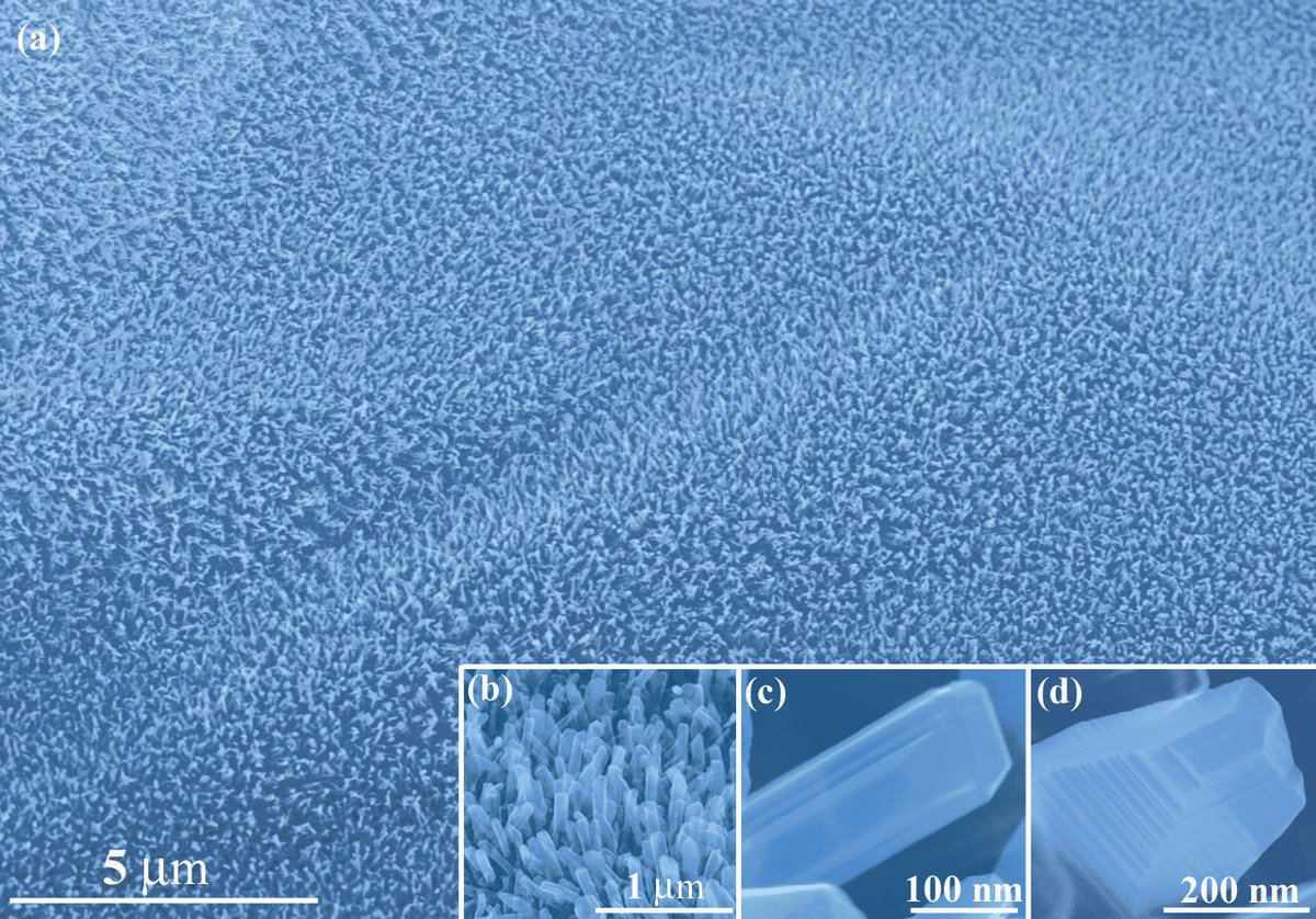
Happy Coral Triangle Day ! 🪸🐠🤿
(June 9)
“Coral reefs”
Coral reefs spread in the sea. These pictures remind us beautiful sight of shiny blue southern ocean are SE (Secondary Electron) images of Si-W-O whiskers using a STEM (Scanning Transmission Electron Microscope) (Fig.a). The whiskers with the size of several hundred nano meters grow all around (Fig.b). One of whiskers has a prism-shape and another has steps of several nano meters on the surface (Fig.c, d). The bright band which extends from the lower left to upper right in the image looks like the sunlight through the seawater.
These works were presented at the "photo contest" hosted by the Japanese Society of Microscopy.
To know more about the image, check out the following post !
3
295
About the latest Variable Pressure SEM, visit hitachi-hightech.com/global/…
101
Happy World Oceans Day ! 🌊🏖🌅🪸🐢🐳
(June 8)
SEM-EDS analysis of Marine Microplastics (MPs)
Microplastics (MPs) fragments collected from a sandy beach were investigated by Variable Pressure SEM. Cross sectional images showed fine inorganic particles with diameters of 0.1 to 1 μm contained in the resin. Compositional analysis result suggested that the MPs is rusted stainless steel (iron-chromium alloy) with anticorrosive paint (chrome yellow).
To know more about the Variable Pressure SEM, check out the following post !
321
About the TEM with Image Navigation Function, visit hitachi-hightech.com/global/…
118
It’s World Food Safety Day ! 🍽🥗🥩🥔🥕🥬🐟
(June 7)
Automated virus particle analysis of negatively stained norovirus
36 TEM images of negatively stained norovirus were automatically acquired using Image Navigation function. Designated areas of a whole grid image or a low magnification image can be automatically imaged at a specified magnification. Particle size distribution of 4096 collected virus particles was measured by batch processing of 36 images using an image processing software, Image Pro Premier.
To know more about the TEM with Image Navigation Function, check out the following post !
1
642
Hitachi Electron Microscope retweeted

"Knock knock, sample delivery!" 🤖🔬
You've seen Aeye-1 at work. Now follow the conversation.
We've added text dialogue to this demonstration, offering a fun new way to explore how the AI-driven transmission electron microscope system autonomously retrieves, transfers, and replaces samples. 🤖🔬
#CAS #AI #Microscopy #ElectronMicroscopy #TEM #AIForScience #MaterialsScience
2
3
320
Read the full story here: hitachi-hightech.com/global/…
101
Happy World Environment Day ! 🌱🌳🌎🌍🌏🌅
(June 5)
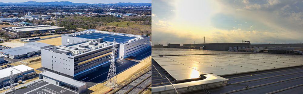
“Reducing CO2 Emissions in Manufacturing Facilities with an Eco-Design Electron Microscope”
It is no exaggeration to say that providing society with products that are in harmony with the environment has become the responsibility of manufacturing companies in recent years. Reducing environmental impact throughout the entire product life cycle—from procurement of raw materials to manufacturing, distribution, use, disposal and recycling—contributes to solving global issues such as climate change, scarcity of water resources, and environmental pollution caused by waste.
Hitachi High-Tech is promoting eco-design throughout the entire Group, with the aim of creating designs that are considerate of the environment right from the initial stages of product development, and quantitatively evaluating their environmental impact through LCA (Life Cycle Assessment).
One of the key elements of this initiative is our global target of reducing CO2 emissions, which is required to achieve carbon neutrality by 2050. Hitachi High-Tech has been promoting manufacturing with lower CO2 emissions by leveraging its unique technologies and expertise cultivated in the course of manufacturing over the years.
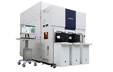
As an example of eco-design, we will look at the High-Precision Electron Beam Metrology System GT2000, the latest model of Hitachi High-Tech's flagship CD-SEMs. A CD-SEM is a metrology tool that measures the quality of semiconductor device patterns formed on silicon wafers at the nanometer-level, making it indispensable to semiconductor manufacturers all around the world.
The latest CD-SEMs possess processing capabilities increased by 25% compared to previous models, while also having reduced CO2 emissions by 50% when compared to our standard product from FY2010. By achieving both improved measurement performance and greatly reduced environmental impact, Hitachi High-Tech is providing robust support to the rapidly expanding semiconductor market that is being driven by advances in generative AI, autonomous driving, next-generation communications and quantum technologies.
To read the full story, check out the following post !
3
385
About BIB (Broad Ion Beam) milling, visit hitachi-hightech.com/global/…
1
130
Happy Oral Health Month ! 😬🦷🪥👄
(June)
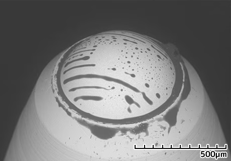
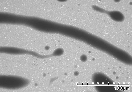
Cross-sectional SEM of a permanent tooth (wisdom tooth)
Cross-sections of a permanent tooth (wisdom tooth) were prepared by BIB (Broad Ion Beam) milling and observed using a Variable Pressure SEM. The two elongated holes in the whole image are root canals containing blood vessels and nerves. The tooth root surface is covered with a cementum layer showing a banded structure like trees thickening with age to form an annual-ring structure. This property has been used to determine the age of mammals. The cross-sectional image of the tooth neck shows the boundary between dentin and enamel. Though distinction between these two has been difficult with a torn surface, ion milled surface allows the identification. Four holes in the enlarged image are cross-sections of dentinal tubules regarded as to transmit pain and temperature.
To know more about BIB (Broad Ion Beam) milling, check out the following post !
3
625
About the latest Low-voltage & Low-vacuum SEM, visit hitachi-hightech.com/global/…
226
Happy National Egg Day ! 🥚🍳🐔
(June 3)
Low-voltage & Low-vacuum SEM of food samples
Various food samples were observed with SEM without coating : fat crystals of chocolate, powder of corn potage, boiled egg yolk, and cross section of buckwheat. Low accelerating voltage SEM and low vacuum SEM revealed their fine crystal structures and surface topography.
To know more about the latest Low-voltage & Low-vacuum SEM, check out the following post !
2
405