
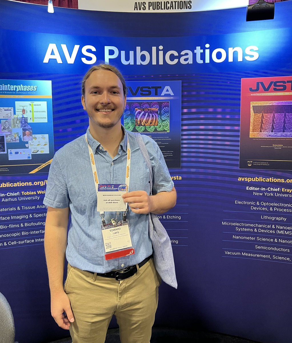
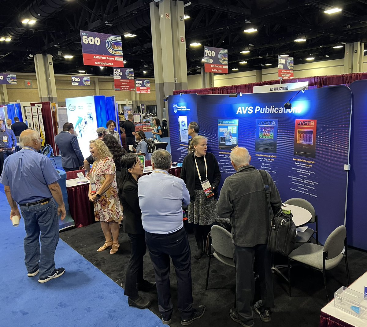
468 Photos and videos


Jun 4
Less heat, less sputtering, more emission—authors from @BallState, @CarnegieMellon & @IndianaAcademy present evidence that nanotubes can fundamentally reshape thermionic cathode performance. Check it out: doi.org/10.1116/6.0005417
17
Jun 3
You've collected the spectrum—now what? Here is your practical guide to making sense of XPS from @CEITEC_Brno.
doi.org/10.1116/6.0005469
14
Jun 2
Machine learning has become essential materials & surface analysis, providing insights into composition, structure & function. @latrobe researchers highlight practical computational choices to achieve faster results exploring #ToFSIMS hyperspectral data. doi.org/10.1116/6.0005335
25
May 26
Anti-glare ITO nanowire-based films, grown at lower temperatures, with tunable wettability & conductivity: a simple & scalable substrate-engineering trick for next-gen optoelectronics.
doi.org/10.1116/6.0005271
17
May 21
Don't know the difference between #JVSTA & #JVSTB? Don't worry, you're not alone!
Check out the full scope of each journal on our websites.
JVST A ➡️ pubs.aip.org/avs/jva/pages/a…
JVST B ➡️ pubs.aip.org/avs/jvb/pages/a…
We can't wait to see what you submit (and to which journal)!
58
May 20
🦥➡️🚀From sluggish to supercharged: plasma-engineered TiVO₄ accelerates green hydrogen reactions. 🍃
doi.org/10.1116/6.0005309
20
May 14
Researchers from @UOsaka_en use atomistic simulations to reveal the double-edged role of ions in plasma #ALDep of silicon nitride: they drive film growth & remove chlorine, but can also bury impurities deeper in the material.
doi.org/10.1116/6.0005302
1
15
May 8
Energy & exposure time of Ar ion bombardment on 2D WSe2 is investigated - researchers from @DukeU discover using the Ar ion beam to modify metal contact interfaces in 2D FETs improves device performance variation at the cost of a reduction in on-current.
doi.org/10.1116/6.0005387
10
May 7
When 2D materials are grown by #MBE, they often have a high density of twin defects.
Check out this study from @UWMadison & @usarmy_devcom on growth conditions of van der Waals material GaSe - showing that at low temps, non-twinned films can be formed.
doi.org/10.1116/6.0005445
21
May 6
By tuning surface chemistry & combining area-selective etching with atomic layer processing, polymer templates can directly guide subsequent selective deposition - highlighting a promising bottom-up route for next-gen semiconductor fabrication. doi.org/10.1116/6.0005294
1
23
May 5
Physics-informed active learning out of @thisisUIC revolutionizes #ALDep pulse tuning - outperforming data-driven methods in speed, accuracy, & precursor use while learning kinetics & enabling automated optimization.
doi.org/10.1116/6.0005430
28
Apr 29
Researchers from @CUBoulderOmbuds get into the nitty-gritty of #ALEtch and watch stress evolve as each reaction step happens - leading to new insights!
doi.org/10.1116/6.0005425
38
Apr 24
What if you could turn up the brightness of a chip like a volume knob? A few clever fabrication tweaks transform a thin film into a light-boosting amplifier & a tiny racetrack for photons—bringing sci-fi-level photonics a step closer to reality.
doi.org/10.1116/6.0005339
1
1
29
Apr 23
Diamonds power quantum tech—but only if their surfaces stay perfect. @Princeton researchers flip #ALEtch to gently smooth diamond at the atomic scale, preserving its quantum magic for next-gen sensors and qubits.
doi.org/10.1116/6.0005266
2
90
Apr 17
Through a case study in #ALDep & #ALEtch, this article shows that structuring review knowledge as machine-actionable graphs complements language models, improving accuracy, consistency, & reproducibility in scientific querying and analysis.
doi.org/10.1116/6.0005226
25
Apr 16
GaN is a material of interest for a wide range of applications. @Cornell authors create lateral devices w/o air exposure using patterned MBE & selective area sublimation, a technique that may enable creation of very complicated devices in the future.
doi.org/10.1116/6.0005402
1
24
Apr 14
Atomic-scale control at surfaces is where materials performance is won or lost & it’s rarely driven by a single mechanism. @penn_state authors dive into how diffusion, reaction kinetics, & energetic particle interactions collide to shape thin film growth.
doi.org/10.1116/6.0005391
1
26
Apr 13
Wafer-scale integration of 2D semiconductors is almost a reality: @FraunhoferIMS & @dresden_ifw show large-area WS₂ films grown by #ALDep & structured directly w/ conventional lithography, w/o sacrificing material quality or continuity across the wafer.
doi.org/10.1116/6.0005225
19
Apr 8
#JVSTA work from @ODU, @Fermilab, & @JLab_News: co-sputtering high-temp annealing achieves desired Nb₃Sn phase w/ controlled Sn content. Result: better film uniformity across complex geometries, one of the key barriers to consistent superconduction.
doi.org/10.1116/6.0005369
21
Apr 8
Introducing: a brand-new liquid Mo precursor! See how simply switching the oxidant flips the pathway to α-MoO₃—and unlocks high-performance photodetectors.
doi.org/10.1116/6.0005336
24