
Atomic Precision: Why $ASMI is the Architect of the 1.6T Nanoworld
In the 1.6T infrastructure era, traditional manufacturing has hit a physical wall.
As the industry pivots to 2nm Gate-All-Around (GAA) transistors, depositing materials atom-by-atom is no longer a luxury - it is the ultimate bottleneck.
ASM International $ASMI has emerged as the gatekeeper of this transition, owning the tools that build the core of AI logic.
1⃣The Machine: Pulsar & Synergis (The ALD Standard)
Atomic Layer Deposition (ALD) is the process of building a chip one atomic layer at a time. For 1.6T networking and AI processors, ASMI’s systems are the industry benchmark:
➡️Pulsar® System: The "Tool of Record" for high-k metal gates. At the 2nm node, it ensures that dielectric layers are perfectly uniform to prevent current leakage in 1000W AI chips.
➡️GAA Architecture: The transition from FinFET to GAA nanosheets requires coating 3D structures that are physically impossible to reach with older methods. ASMI's ALD technology wraps the gate around the channel with angstrom-level precision, enabling the energy efficiency required for the 1.6T cycle.
➡️Epitaxy Synergy: ASMI's Intrepid® and Synergis® systems handle the critical "growing" of silicon-germanium layers for nanosheets, providing a dual-threat capability in both deposition and crystal growth.
2⃣ The Strategic Pivot: Area Selective Deposition (ASD)
ASMI has successfully moved Area Selective Deposition (ASD) from the lab to High-Volume Manufacturing (HVM).
The Breakthrough: ASD allows materials (like Molybdenum or advanced insulators) to "grow" only on specific chemical surfaces, eliminating the need for several costly lithography and etching steps.
1.6T Impact: Selective ALD reduces "edge placement errors" (EPE), which are the primary cause of signal noise in 224G-per-lane networking. ASMI currently holds a near-monopoly on the first wave of ASD tools deployed in 2nm fabs.
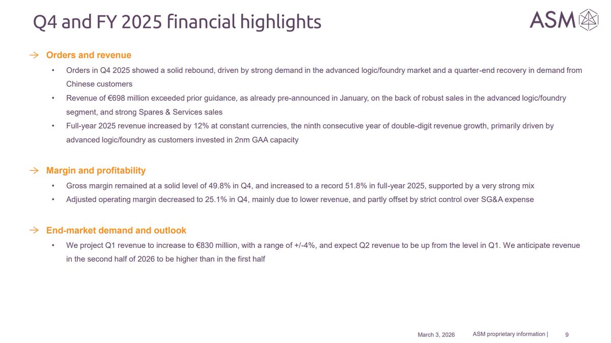
3⃣Investor Proof Points: Financial Reality ( last report 3rd March 2026)
Record Revenue: ASMI ended 2025 with record revenue of €3.2 billion (up 12% at constant currencies), driven primarily by the 2nm GAA ramp-up.
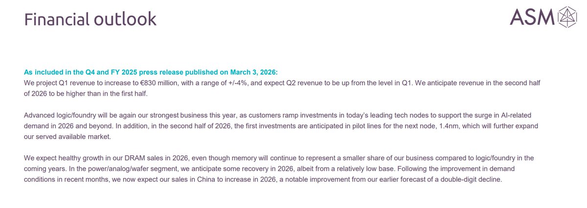
Q1 2026 Guidance: Management officially projected Q1 2026 revenue of €830 million ( /- 4%), with a clear outlook for a stronger second half of 2026 as HBM4 memory orders accelerate.
Order Momentum: Q4 2025 bookings hit €803 million, significantly beating consensus estimates and signaling a massive rebound in logic/foundry demand.
Capital Return: The board has proposed an increased dividend of €3.25 per share (to be approved May 11, 2026) and a new €150 million share buyback program for 2026/2027.
4⃣ Competitive Moat: ASMI vs. The Giants
While Applied Materials $AMAT and Tokyo Electron are formidable, ASMI's niche focus gives it a tactical edge in the 1.6T stack:
The ALD Lead: ASMI controls over 55% of the global ALD market for logic. While AMAT is a leader in etch and CVD, ASMI’s "narrow and deep" expertise in atomic layers makes them indispensable for the 2nm gate stack.
Silicon Carbide (SiC) Recovery: Through its LPE subsidiary, ASMI is seeing a recovery in SiC epitaxy tools as AI data centers move toward more efficient power delivery systems, diversifying the company away from pure logic.
Final Verdict: The 2nm Yield Arbiter
ASMI is no longer a "growth story" - it is a Yield Arbiter. Without ASMI’s ALD and selective deposition, the 2nm node simply does not work.
Summary: The 1.6T era is defined by extreme density. By solving the patterning and insulation crises at the atomic level, $ASMI has secured its place as a mandatory partner for TSMC, Intel, and Samsung. For investors, ASMI represents the most direct way to play the materials science revolution that underpins the next decade of AI hardware.
#ASMI #ALD #Semiconductors #1_6T #2nm #GAA #Investing2026 #HighTechManufacturing #ASMLPartner


The Reliability Guard: Why $AEHR is the Invisible Gatekeeper of the AI Supercycle
In the high-stakes race for AI dominance, the industry has hit a physical wall: Thermal Infantile Mortality.
As chip power consumption moves toward the kilowatt range, the risk of "dead on arrival" hardware has become a multi-billion dollar liability.
Aehr Test Systems $AEHR has positioned itself as the only scalable solution to this bottleneck, transitioning from a niche Silicon Carbide player into a fundamental pillar of the 1.6T networking and AI ASIC supply chain.
1⃣The Core Edge: Torturing Silicon at 3,500 Watts
Modern AI processors and 1.6T optical chips are power-hungry monsters. Traditional "single-die" testing is now too slow and costly. Aehr has changed the rules with its FOX-XP Ultra-High Power system:
Extreme Power Density: These systems deliver and dissipate 3,500 Watts per wafer across nine 300mm wafers simultaneously an industry record.
Multi-Zone Thermal Control: Each wafer is divided into independent thermal zones, allowing the system to catch "infant mortality" defects without melting the delicate silicon structures.
1.6T Synergy: New March 2026 orders for Silicon Photonics configurations ensure that even the smallest crystal defects are caught before packaging, saving giants like Broadcom and Intel billions in potential losses.
2⃣The "Razor & Blade" Revenue Engine: More Than Just Machines
Investors often misjudge AEHR by looking only at large system contracts. Its true strength lies in its high-margin, recurring revenue model:
The Razor (FOX-XP/Sonoma): Selling the system is the "entry ticket" to the customer’s fab.
The Blade (WaferPak™ & DiePak®): Every new chip architecture (e.g., the transition from Nvidia Blackwell to Rubin) requires a new, proprietary set of WaferPaks.
Recurring Alpha: During production ramps, these consumables generate gross margins exceeding 60%, providing a financial cushion against the cyclical nature of hardware sales.
Strategic Expansion: With the integration of Incal Technology, Aehr now earns twice: first by testing the wafer, and then the packaged module.
3⃣Financial Deep-Dive: The Great Inflection
March 2026 marks the moment Aehr shifted from "promise" to "execution":
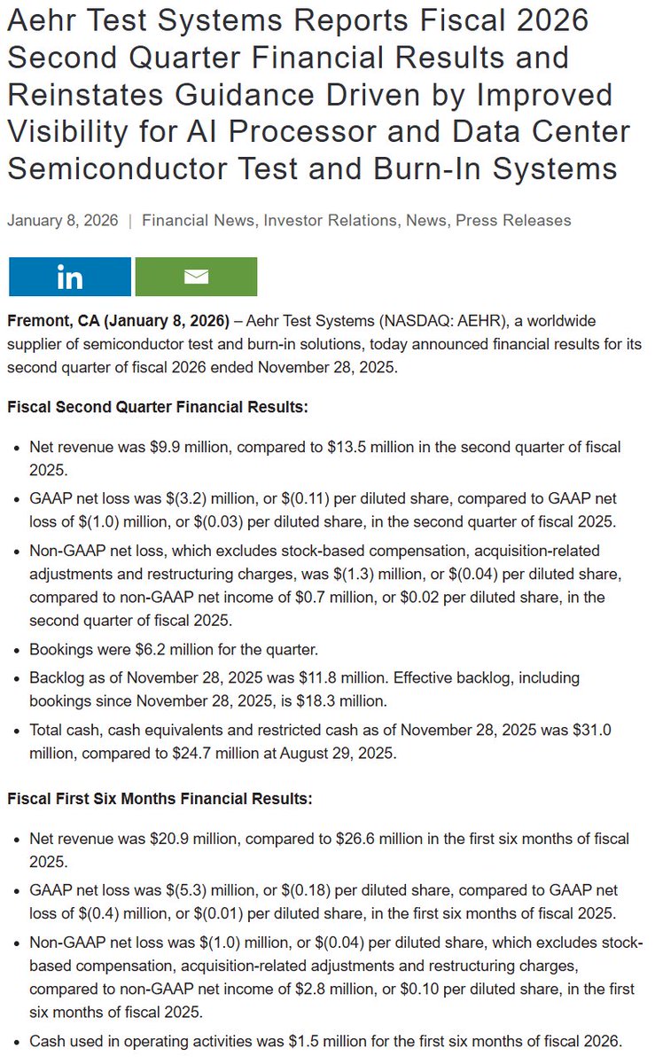
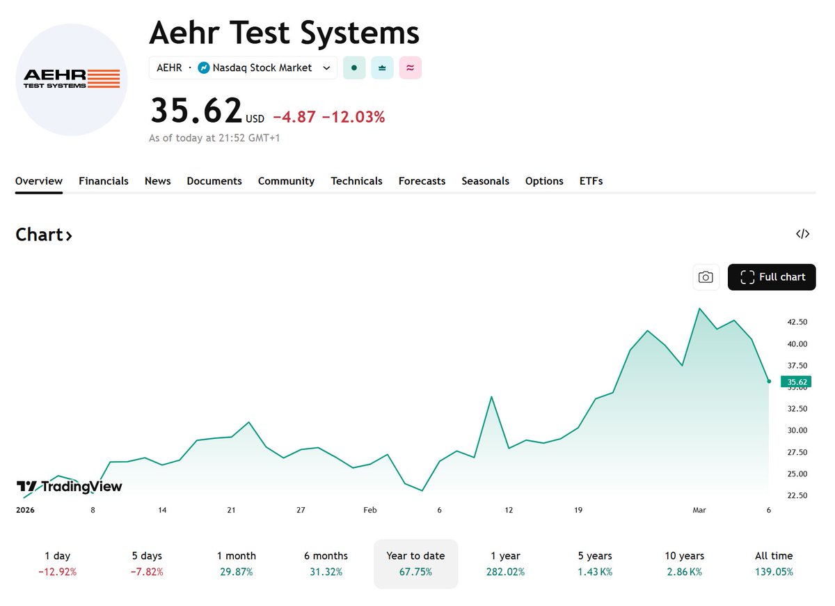
The Guidance Pivot: In January 2026, the company reinstated guidance, targeting $25M–$30M in H2 FY26. A recent $14M order from a lead AI customer proves these targets are within reach.
Backlog Visibility: While the current backlog is $18.3M, management expects bookings of $60M–$80M in the coming months, setting the stage for a record-breaking FY2027.
Ironclad Balance Sheet: With $31.3M in cash and zero debt, Aehr has the liquidity to scale production rapidly for the 1.6T era.
Institutional Momentum: A double upgrade from William Blair and increased stakes from firms like Wellington Management confirm that "smart money" has identified the bottom.
4⃣ The Specialist vs. The Giants: Can $AEHR Scale?
The ultimate question for $AEHR is how it survives in a market dominated by Advantest and Teradyne.
Specialization vs. Scale: Advantest and Teradyne control ~95% of the general ATE (Automated Test Equipment) market. However, they lack Aehr’s hyper-specific expertise in ultra-high-power wafer-level burn-in. For AI chips pulling 1000W , generalist tools are insufficient.
The Acquisition Narrative: With a market cap around $1.3B and a year-to-date gain of 118% (as of March 6, 2026), Aehr is increasingly viewed as an acquisition target. Its proprietary Sonoma and FOX-XP platforms would be a perfect "bolt-on" for Advantest to complete its AI testing suite.
Market Potential: While today’s revenue is small, William Blair estimates a $1.5B–$2.3B Total Addressable Market (TAM) for AI burn-in tools by 2030. If Aehr captures even 30% of this niche, its fair value could reach $50–$70 per share.
Final Verdict: The Strategic Inflection Point
Aehr Test Systems is no longer a speculative play on electric vehicles; it is a fundamental tax on AI reliability.
The Bull Case: Aehr owns the only high-volume platform for 3,500W wafer-level testing. As hyperscalers like Alphabet and Amazon commit hundreds of billions to AI infrastructure in 2026, the demand for "guaranteed uptime" makes Aehr’s technology an operational necessity.
The Bear Case: Customer concentration remains high. A delay in the Silicon Photonics ramp would hurt. However, with the launch of the Sonoma system, Aehr is successfully diversifying into the broader AI ASIC and memory markets.
Conclusion: Aehr is the gatekeeper. As AI power envelopes push toward the physical limits of silicon, Aehr’s ability to "torture-test" at scale makes it an indispensable component of the 1.6T stack. For investors, the play is no longer about "testing".
It is about Yield Assurance in a world where failure is not an option.
#AEHR #AIInfrastructure #Semiconductors #Investing #BurnInTesting #Advantest #Teradyne #MarketAnalysis

1
5
29
10,723