
23 Dec 2025
Are you using graphene for your research?
Nanosurf's DriveAFM can help you with that!
Applications include:
- Surface characterization: Measure roughness, layer thickness, and defects with sub-nanometer precision
- Electrical mapping: Use conductive AFM to probe local conductivity and work function
- Mechanical testing: Quantify stiffness and adhesion at the nanoscale
- Manipulation & patterning: Move flakes, apply force, or even write patterns with the tip
- Environmental control: Study samples inside gloveboxes or under controlled humidity/gas
Whether you're working on sensors, transistors, or coatings, AFM gives you the resolution and flexibility to push graphene research forward.
Read our application note: hubs.la/Q03NFS7c0
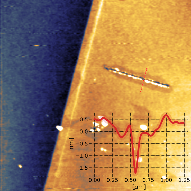
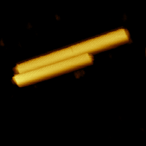
Image: Cutting graphene by AFM lithography. AFM topography image of a multilayer graphene flake on Si substrate with lateral dimensions of 10 x 10 µm2
#AFM #graphene #nanotechnology #Nanosurf
2
134
16 Dec 2025
Struggling with characterizing polymers?
You need a method to understand their surface properties in short time without compromising data quality.
👉 The solution is Nanosurf’s DriveAFM with WaveMode NMA: fast elasticity maps at high resolution!
WaveMode NMA works through photothermal excitation of the cantilever and is available exclusively on our DriveAFM and industrial systems with the CleanDrive module.
💪Only looking for topography? WaveMode can obtain an image 15x faster than conventional dynamic mode in ambient conditions. WaveMode is the fastest off-resonance AFM mode available on the market.
To know more, read our blog article: hubs.la/Q03XdM5R0
In the image: Elasticity map of SBS-PS polymer blend measured with WM0.8PTD cantilever in WaveMode NMA. Color range 200 MPa to 3 GPa (log scale), 3 μm scan size, 500 x 500 px, 25 kHz WaveMode excitation frequency
1
2
135
2 Dec 2025
Have you ever thought of how polymers changed the world?
They are known for their presence and importance in many everyday objects, from OLED phone screens to plastic food containers. But bottlebrush polymers - made of one central backbone and many side chains - may be less known. Their unique architecture enables applications in elastomers, photonics, and biomedical devices.
The challenge is to imaging bottlebrush polymers at molecular resolution. Conventional AFM struggles with slow speed and sample drift, which result in blurred image.
Do you want to be get rid of drift effects and visualize side chains of polymers? WaveMode on DriveAFM is the answer:
☑️ 15 faster than dynamic mode in ambient conditions → reduces effect of drift in images
☑️ Off-resonance photothermal excitation → precise force control
☑️ High-resolution imaging → count side chains of polymers
Read more about how WaveMode helps imaging polymers: hubs.la/Q03Wdv_f0

2
106
27 Nov 2025
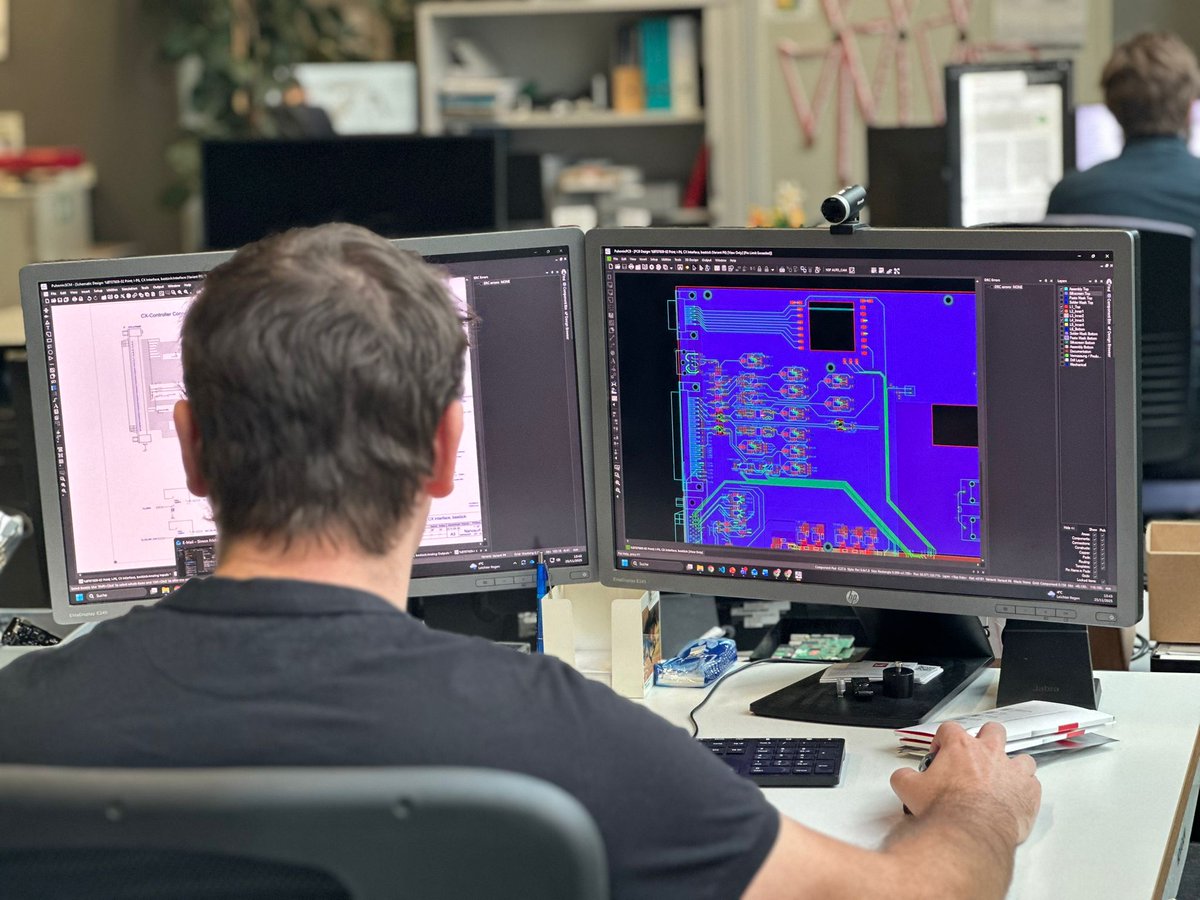
Nanosurf #BehindTheScenes! How is the electronics of our AFMs developed?
Our electrical engineers carefully design the circuits of the DriveAFM and all other Nanosurf products. Their technical expertise is essential for developing high-res scientific instruments capable of delivering reliable and accurate data of the world at the nanoscale.
Whether for #biomedical research, the #semiconductor industry, or #materialScience, DriveAFM delivers outstanding performance.
Did you know? DriveAFM can operate in WaveMode, up to 15× faster than traditional dynamic mode in ambient conditions, while maintaining impressive sub-nm resolution.
Discover more 👉 hubs.ly/Q03VXwxF0
2
100
25 Nov 2025
For reliable atomic force microscopy (AFM) on delicate samples, it is crucial to control forces down to below 100 pN.
One example of such a sample is tobacco mosaic virus (TMV), which collapses if excessive force is applied.
Traditional dynamic (tapping) mode did not allow the required level of force control, but NanoSurf has found the solution: WaveMode, the off-resonance technique available on our DriveAFM and on the industrial solution Alphacen 300 Drive.
In WaveMode, an additional laser excites the cantilever via the photothermal effect. The WaveMode signal can be translated into a force in Newton, which it also allows fast imaging in air and in liquid with precisely defined tip-sample interaction. WaveMode is the fastest off resonance AFM technique available.
Want to know more about the high resolution imaging of TMV? Read our blog: hubs.la/Q03VBLc_0
1
2
125
18 Nov 2025
Metal alloys have accompanied humans from the Bronze Age, and today they drive innovation in several fields.
For advanced semiconductor applications, it is fundamental to characterize metal alloys at nanoscale, and to make sure they have the right properties. Thanks to its versatility and precision, atomic force microscopy is the perfect technique to tackle this challenge.
Now, Nanosurf's DriveAFM can deliver the highest image quality at unprecedented speed, thanks to its unique WaveMode, the fastest off-resonance AFM technique on the market. Joined with our FastScanning add-on, it can scan areas of many square microns with 512 x 512 pixels in under 35 s!
And if you need accurate nanomechanics measurements, our DriveAFM can perform WaveMode NMA: quantitative, easy to use, fast.
☑️ WaveMode → fastest off-resonance AFM mode on DriveAFM.
☑️ WaveMode NMA → quantitative elasticity topography in one scan.
☑️ Visualize phase variations quickly and accurately.
Curious to read more? Here it is our blog article on metal alloy measurements: hubs.la/Q03RQDSc0

3
114
11 Nov 2025
Do you know the impact of surface roughness on silicon wafers?
Seminconductor researchers and manufacturers constantly keep an eye on the roughness of their silicon wafers at sub-nanometer scale. A rough wafer scatters charge carriers, driving up resistance and cutting efficiency, which might impair high-performance CPUs, GPUs, and memory chips.
Atomic Force Microscopy is the ideal instrument to perform quality controls on your wafer! Want to speed it up?
With our DriveAFM, you can use WaveMode, the fastest off-resonance AFM technique!
☑️15× faster than conventional AFM in ambient condition → high throughput.
☑️Available on DriveAFM and Alphacen 300 Drive.
☑️Precise force control → reproducibility, minimal tip wear.
Read our blog article to find out more: hubs.la/Q03SqJX60
In the picture: Surface of a silicon wafer imaged with DriveAFM using WaveMode. The whole image of 512 pixel x 512 pixel (1 μm x μm) took less than 34 seconds to be acquired.
2
63
4 Nov 2025
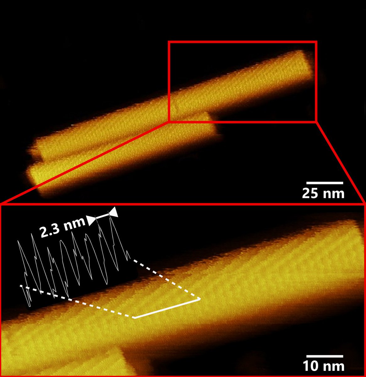
Have you ever heard of tobacco mosaic virus (TMV)?
Irregular, mottled, mosaic-like pattern on the leaves, yield loss and stunted growth. In the Thirties, the discovery of this plant virus and its crystallization marked the beginning of molecular virology.
Yet, it remained an open challenge to image TMV at high resolution in its physiological (humid, liquid) environment... until now!
Thanks to WaveMode on the DriveAFM by Nanosurf, it is possible to obtain a high-resolution image of TMV in liquid.
WaveMode is the fastest off-resonance AFM technique:
☑️Resolves TMV’s periodic 2.3 nm texture without damaging the sample.
☑️Operates in liquid, preserving native conditions.
☑️Off-resonance imaging → precise force control
Want to know more? Read our blog post: hubs.la/Q03RqKJH0
1
2
157
28 Oct 2025
Do you know how the fastest off-resonance AFM technique on the market works?
Nanosurf’s WaveMode enables accurate and gentle measurements, achieving speeds up to 15 times faster than traditional dynamic mode in ambient conditions. But how is this possible?
WaveMode is possibile thanks to an additional laser that photothermally excites the cantilever. This laser, provided by the CleanDrive module, is usually focused near the base of the cantilever and modulated in amplitude. This approach removes the limitations imposed by resonance bandwidth, allowing for faster imaging and quantitative force control.
WaveMode is available only on our high-end DriveAFM and the industrial-grade Alphacen 300 Drive.
Interested in learning more? Read our technical note: hubs.la/Q03QmHMx0
1
3
115
23 Oct 2025
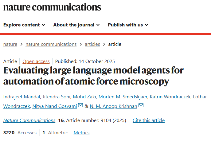
AFM and AI... it sounds like an interesting match, doesn't it?
We’re thrilled to see our high-end DriveAFM featured in a study published in @Nature Communication by Nitya Nand Gosvami
"Evaluating large language model agents for automation of atomic force microscopy"
In this work, researchers introduced AILA (Artificially Intelligent Lab Assistant), a large language model (LLM)-powered framework designed to automate complex AFM workflows. Using Nanosurf's DriveAFM as the experimental platform, the team demonstrated how AI agents can perform tasks ranging from graphene layer counting to friction characterization on HOPG, all with minimal human intervention.
This study not only showcases the versatility of our DriveAFM instruments but also marks a significant step toward self-driving laboratories in materials science.
Discover the instrument behind this work: hubs.la/Q03PhvVq0
👏 Congratulations to the authors!
#AFM #AI #Nanosurf
3
115
21 Oct 2025
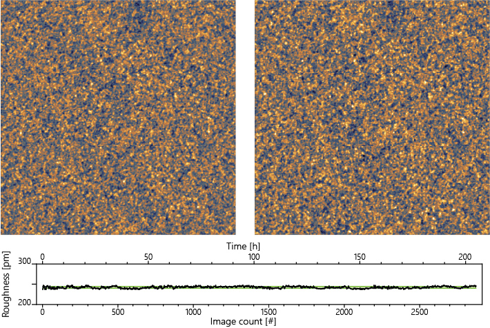
How do you estimate the sub-nanometer roughness of your silicon wafer?
The surface properties of silicon wafers have a significant influence on the property of the material, and affect the efficiency and reliability of the final device.
One of the best technique to monitor roughness in a precise, accurate and repeatable way is atomic force microscopy (AFM). Now, with Nanosurf's WaveMode, AFM even gets 15 times faster!
WaveMode is the fastest off resonance AFM mode existing. An additional laser excites the cantilever by phototermal effect, allowing to overcome the traditional limits of dynamic mode.
It allows a precise control of the force applied, ensuring reproducible results, cross-tool comparability, and reduced tip wear. In the picture, a time-series of surface roughness measurements of a silicon wafer using WaveMode over 9 days.
WaveMode is available only on our DriveAFM, and the industrial solution Alphacen 300 Drive.
Curious to know more? Read our blog article: hubs.la/Q03PkClZ0
#AFM #WaveMode #nanoscience
1
3
118
14 Oct 2025
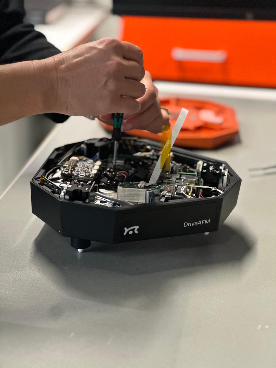
Nanosurf #BehindTheScenes! How is our DriveAFM made?
Our skilled technicians hand-assemble every #AFM here in Switzerland, carefully testing and fitting each component one by one. It’s a meticulous process reminiscent of Swiss watchmaking, but our instruments are packed with cutting-edge technology.
Whether for #biomedical research, the #semiconductor industry, or #materialScience, DriveAFM delivers outstanding performance.
Did you know? DriveAFM can operate in WaveMode, up to 15× faster than traditional dynamic mode, while maintaining impressive sub-nm resolution.
Discover more 👉 hubs.la/Q03Nr72Z0
2
71
9 Oct 2025
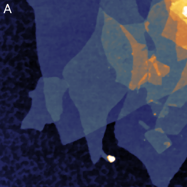
Silicene, phosphorene, germanene, stanine.. who's working with a 2D material?
The most popular is surely graphene, a sheet of covalently bonded carbon atoms with the highest known thermal and electrical conductivity.
Our DriveAFM is an amazing tool to study graphene:
- Atomic-scale resolution: ~0.1 nm vertical, few nm lateral
- Multimodal measurements: Topography, electrical & mechanical properties acquired simultaneously
- Nanoscale manipulation: Use the tip to move or modify samples
- Compact design: Fits inside a glovebox for controlled environments
Curious how DriveAFM can boost your graphene research?
👉 Read our application note: hubs.la/Q03MLkQH0
Image: AFM topographical image of graphene oxide with lateral dimensions of 5.11 x 5.11 µm2
Sample courtesy of Nanotech Energy, USA
#graphene #nanoscience #AFM #Nanosurf
1
3
126
2 Oct 2025
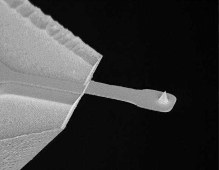
What makes you say "this is the right probe" for your AFM experiment? 🤯
Whether you're imaging DNA origami, measuring polymer mechanics, or mapping the elasticity of metal alloys, the right cantilever makes all the difference.
At Nanosurf, we’ve developed a Probe Guide to help you select the best cantilever for WaveMode, the fastest off-resonance tapping technique available exclusively on DriveAFM.
Here's some advices to run WaveMode at its best:
WM0.1Au-SS: Ultra-soft for biomolecules, enabling forces <100 pN
WM0.3Al: Ideal for industrial roughness measurements with high wear resistance
WM0.8PTD: High amplitude imaging for polymers and 2D materials
WM20PTD: Fast scans of hard samples with elasticity mapping up to 50 GPa
See the topography images, elasticity maps, and more in the full guide: hubs.la/Q03LHBFv0
What are your advices? Write them in the comments 👇
#Nanoscience #Nanotechnology #Nanosurf #AFM
1
3
116
16 Sep 2025
This application note presents a detailed study of normal alkanes using DriveAFM, focusing on their lamellar structures and crystallization behaviors.
Learn more in the full application note!
🔗 hubs.la/Q03GkRyr0
1
2
104
29 Jul 2025
This application note presents a detailed study of normal alkanes using DriveAFM, focusing on their lamellar structures and crystallization behaviors, particularly when chain lengths exceed 120 units, leading to chain folding—a key aspect of polymer crystallization.
Using highly oriented pyrolytic graphite (HOPG) as a substrate, the study explores the 2D organization of alkanes, showing how they form ordered structures and how their molecular orientation and lamellar width change. AFM images captured at room temperature reveal intricate details of the lamellar edges formed by -CH3 end groups, as well as the overall topography of these lamellar sheets. The application note also investigates the behavior of these alkanes above their melting points, providing valuable insights into the nanoscale features of alkane crystallization.
🔬 Why it matters:
DriveAFM offers unique insights into the crystallization behaviors and nanoscale organization of alkanes, enhancing our understanding of polymer materials and their applications in various industries.
Learn more in the full application note!
🔗 hubs.la/Q03tBcd90
1
2
171
1 Jul 2025
📣Nanosurf and the DriveAFM are on the move for a week of conferences!
This week, Nanosurf is heading to four major conferences across life sciences, materials science, semiconductors, and advanced microscopy. We’d love to connect with you at these events:
• 19th Meeting of the French Microscopy Society in Toulouse:Carolina Paba (Application Scientist) and Marco Portalupi (Sales Manager) will be at the booth with a DriveAFM, running live measurements and available for discussions. Take the opportunity to see the DriveAFM in operation and connect with our team.
• MMC2025 in Manchester: Join David Morgan (Sales UK), Colin Grant and Héctor Corte-León(Application Scientists) for hands-on DriveAFM demonstrations. Bring your questions or samples, explore Hector’s poster on nanomechanics with WaveMode, and attend our presentations throughout the event.
• 15th European Biophysics Congress in Rome: Meet Christian Bippes (Product Manager) from Nanosurf and Stefano Pergolini (Sales Manager) from QuantumDesignItaly. They’re available to discuss your research needs and how the DriveAFM can help advance your work.
• UK Semiconductors in Sheffield: Connect with our Head of Sales, Jens Böttcher, for insights on AFM-based metrology in semiconductors and answers to your technical questions.
#AFM #SPM #nanosurf #DriveAFM #MMC2025 #EBSA2025 #SFµ2025 #UKsemiconductors
1
2
113

23 Apr 2025
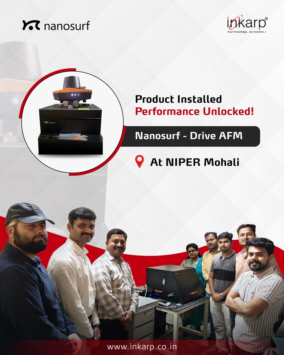
Successful installation & demo of Nanosurf DriveAFM at NIPER, Mohali! Kudos to our expert team trained in Switzerland. Wishing the researchers great discoveries ahead!
🔬 Nanotech | AFM | Nanoindentation
📩 info@inkarp.co.in
#DriveAFM #Nanotech #NIPERMohali #AFM #Inkarp
1
2
37
22 Apr 2025
This application note explores the fascinating self-assembly of semi-fluorinated alkanes on Silicon, HOPG, and MoS2 substrates using DriveAFM.
🔗 hubs.la/Q030Mt760
1
3
144
8 Apr 2025
This application note presents a detailed study of normal alkanes using DriveAFM, focusing on their structures and behaviors, particularly when chain lengths exceed 120 units, leading to chain folding—a key aspect of polymer crystallization.
🔗 hubs.la/Q030MtzQ0
1
3
169