Francis mithika retweeted

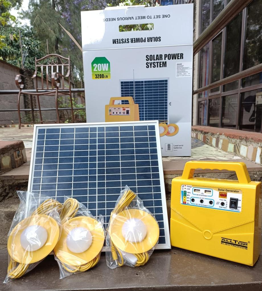
𝟐𝟎𝐖𝐀𝐓𝐓𝐒 𝐒𝐎𝐋𝐀𝐑 𝐏𝐎𝐖𝐄𝐑 𝐒𝐘𝐒𝐓𝐄𝐌
LED Bulb: 5W bulb 3pcs, with 5m cable,6000K
Solar Panel: 18V 20W, Polycrystalline
Battery Type: lithium-ion battery 18AH 3.2V
Charging time: 6-8 hours
Discharging time: 10-24 hours
LED: 160 lm/w
Radio: Support FM radio function/U disk/SD card
Material: ABS
System Host Size: 180*80*204mm
Solar Panel Size: 341*340*18mm
Warranty: 2 years
Kshs10,500/=
WhatsApp No. 0754212159
#BushSolarLightsDelivers
Sent from WA Business
wa.me/254711646690?source=ex…

1
38
Gideon Kitheka Snr retweeted
𝟐𝟎𝐖𝐀𝐓𝐓𝐒 𝐒𝐎𝐋𝐀𝐑 𝐏𝐎𝐖𝐄𝐑 𝐒𝐘𝐒𝐓𝐄𝐌
LED Bulb: 5W bulb 3pcs, with 5m cable,6000K
Solar Panel: 18V 20W, Polycrystalline
Battery Type: lithium-ion battery 18AH 3.2V
Charging time: 6-8 hours
Discharging time: 10-24 hours
LED: 160 lm/w
Radio: Support FM radio function/U disk/SD card
Material: ABS
System Host Size: 180*80*204mm
Solar Panel Size: 341*340*18mm
Warranty: 2 years
Kshs10,500/=
WhatsApp No. 0754212159
#BushSolarLightsDelivers
Sent from WA Business
wa.me/254711646690?source=ex…
3
2
64

We get asked this question often, does geothermal have a turbine shortage like gas? No.
Geothermal turbines operate at much lower temperatures (~150-250 C) than gas turbines (1300 C), and can be forged with conventional polycrystalline steels, of which thousands of foundries can do so globally, in contrast to <10 foundries that can cast the superalloy monocrystalline blades for gas turbines.
Even as geothermal scales like gas, we won't run into this bottleneck bc of our simplicity and the deep bench of foundries we can tap. The hard part for geothermal is not the topside, it's the bottomside.
Jun 14

Order a large gas turbine today and the slot you're quoted runs into 2029 or 2030. GE Vernova has 100 GW on contract, because data centers booked the factory dates first.
That changes how a power plant gets built. The schedule no longer starts with the permit or the construction, it starts with the slot the manufacturer gives you. That date is the fixed bar on the Gantt chart, and everything else is scheduled backward from it.
utilitydive.com/news/ge-vern…

3
6
43
5,627

Jun 14
Jokes aside
Square silicon substrates for packaging do exist
Mitsubishi Materials has produced 510mm x 510mm square silicon panel substrates in 2024
Now, these are not made by using the Czochralski process, which creates a super-high-purity monocrystalline silicon boule
Mitsubishi's columnar silicon is made by casting high-purity silicon and directionally solidifying it, and it is polycrystalline with grain boundaries
These are not suitable for transistor production because they are not that pure (7N vs 11N), but they can absolutely be used as substrates for advanced packaging


Jun 14

Stacy has created a new process for creating cuboidal silicon ingots called the Rasgon process
It's a huge upgrade over the traditional Czochralski (CZ) process

6
14
190
41,270

Jun 14
Researchers may have found a new materials-design route around a core spintronics bottleneck: keep the low-resistance benefits of a good metal while locally breaking inversion symmetry enough to generate unusually large spin Hall conductivity.
That is the real breakthrough: not magic zero-loss spin current, but high charge conductivity very large charge-to-spin conversion in the same material platform.
First, tighten the factual baseline
The result is real and recent. The Nature Materials paper, published June 12, 2026, reports polar nano-regions in metallic PtCoO₂ and says these polar lattice distortions enhance charge-to-spin conversion by two orders of magnitude compared with the non-polar phase. The authors report a room-temperature spin Hall conductivity of 1.6 × 10⁷ ℏ/2e (Ω m)⁻¹, use electron ptychography to connect the inversion-symmetry breaking to local polar nano-regions, and show spin–orbit torque switching with reduced switching voltage and power versus Pt-based control devices.
PtCoO₂ is an unusually good host for this idea because it is already known as an ultrahigh-conductivity delafossite metal. Earlier work describes PtCoO₂ and PdCoO₂ as quasi-two-dimensional metals with extremely long mean free paths and remarkably high electrical conductivity; PtCoO₂ has even been described as having a room-temperature mean free path longer than elemental Cu or Ag in certain comparisons.
There was also theoretical groundwork: a 2018 theoretical paper predicted a strong intrinsic spin Hall effect in two-dimensional metallic PtCoO₂, tied to electronic-structure features near the Fermi surface and strong spin–orbit coupling. The new Nature Materials paper is important because it moves the story from “PtCoO₂ should be interesting” to “we can engineer polar distortions inside a highly conductive metal and experimentally boost charge–spin conversion.”
Key correction to your wording
Replace:
“A metal can now generate strong spin currents without wasting energy as heat.”
With:
“A highly conductive metal can now generate unusually strong spin Hall currents with much lower ohmic loss than many conventional high-spin-conversion materials.”
That one edit matters because no real current-carrying device has zero Joule heating. The claim is not “no heat.” The claim is less wasted heat for a useful spin torque, because the material keeps metallic conductivity while producing much stronger spin conversion than the non-polar version.
Also, do not blur spin Hall conductivity with spin Hall angle. Spin Hall conductivity tells you how much spin current you generate per electric field. Spin Hall angle or damping-like torque efficiency tells you how much spin torque you get per charge current in a real device stack. Both matter. The Nature paper’s headline number is spin Hall conductivity, plus device switching improvements, which is strong; but practical MRAM engineers will still ask for spin Hall angle, spin diffusion length, interface transparency, write-current density, endurance, and wafer-scale reproducibility.
Better version of the post
Scientists may have opened a new route around one of spintronics’ biggest materials trade-offs.In spintronic memory and logic, the goal is to turn ordinary charge current into spin current efficiently, so electron spin can switch magnetic bits with less energy.The problem: many materials with strong spin Hall conversion are resistive, so they waste energy as heat. Many good metals conduct well, but do not generate enough spin current.Now a team has shown that polar nano-regions inside metallic PtCoO₂ can change that balance. These tiny local lattice distortions break inversion symmetry and act like nanoscale spin-current generators, while the crystal keeps its overall metallic conductivity.The result: a reported room-temperature spin Hall conductivity of 1.6 × 10⁷ ℏ/2e (Ω m)⁻¹, roughly two orders of magnitude stronger charge–spin conversion than the non-polar phase, plus lower-voltage spin–orbit-torque switching compared with Pt controls.The deeper point is not just “better PtCoO₂.”The deeper point is a new design principle: engineer local symmetry breaking inside a good metal instead of choosing between high spin conversion and low resistance.If this scales, it could influence future spin–orbit-torque MRAM, low-power magnetic logic, and maybe even interconnect-adjacent spintronic devices.
The strongest thesis
Use this:
This work suggests spintronics can move from “find a lucky heavy metal” to “engineer nanoscale symmetry inside a conductor.”
That is the genius framing.
For years, spin-source materials were stuck between two design goals that fought each other. You wanted strong spin–orbit coupling and broken symmetries to generate spin current, but you also wanted clean metallic transport to avoid heat. PtCoO₂ with polar nano-regions is interesting because it says: do not destroy the metal; distort it locally.
That is a very different mindset.
What actually changed physically
A normal charge current moves electron charge through a material. In a material with strong spin–orbit coupling, the motion of charge can generate a transverse flow of spin angular momentum: the spin Hall effect. That spin current can then apply a torque to a nearby magnetic layer, switching its magnetization.
The old problem was that many strong spin Hall materials had high resistivity. That means you could get good spin conversion, but you paid for it with Joule heating. PtCoO₂ is different because it already conducts extremely well, and the new work introduces local polar distortions that break inversion symmetry without fully wrecking the metal’s clean transport.
The phrase polar nano-regions is doing a lot of work here. These are not necessarily giant macroscopic ferroelectric domains. They are tiny local regions where atoms shift in a way that creates local polarity. In a metal, that is surprising because free electrons usually screen electric polarization. So the deep materials idea is: you can have local polarity coexisting with metallic conduction, and that local symmetry breaking can amplify spin-current generation.
Missing elements that would make the story much stronger
The biggest missing element is the full device figure of merit. The post focuses on spin Hall conductivity, but practical devices care about switching energy per bit, write voltage, current density, pulse duration, endurance, thermal stability, and retention. The Nature paper reports reduced switching voltage and power relative to Pt controls, which is highly relevant, but the viral version should say “device-level energy reduction” rather than just “strong spin currents.”
The second missing element is spin Hall angle or damping-like torque efficiency. A material can have high spin Hall conductivity and still need careful interpretation if its charge conductivity is also huge. Engineers will ask: how much spin torque do I get per unit charge current in the actual stack?
The third missing element is spin diffusion length. Generating a spin current is not enough. The spin current has to survive long enough to reach the magnetic layer and transfer angular momentum efficiently.
The fourth missing element is interface transparency. Spin current can be generated in PtCoO₂, but if the PtCoO₂ / ferromagnet interface reflects or absorbs it badly, the device benefit shrinks. Interface engineering may be just as important as the bulk material.
The fifth missing element is how the polar nano-regions are created and controlled. Are they strain-induced? Growth-induced? Oxygen-stoichiometry-related? Thickness-dependent? Substrate-dependent? Random? Tunable? A design principle only becomes a technology when you can control it.
The sixth missing element is stability under device operation. Do the polar nano-regions survive current pulses, heat, electromigration, cycling, and manufacturing steps? A spintronic memory material has to work billions to trillions of times, not once in a lab measurement.
The seventh missing element is wafer-scale reproducibility. “Compatible with silicon substrates” is promising, but industry will ask whether the effect survives large-area growth, patterning, lithography, etching, annealing, and integration with standard magnetic tunnel junction stacks.
The eighth missing element is comparison against the real industrial baselines: Pt, β-W, β-Ta, Pt alloys, topological insulators, Weyl semimetals, PtTe₂, BiSb, and other high-SOT materials. The right question is not “is the spin Hall conductivity large?” It is: does PtCoO₂ beat the best alternatives at equal thickness, equal magnetic layer, equal pulse length, equal thermal stability, and equal manufacturing constraints?
The ninth missing element is cost and supply chain. PtCoO₂ contains platinum and cobalt. That does not kill the technology, because spintronic layers can be very thin, but it matters for scaling, sourcing, and cost.
The tenth missing element is logic vs memory realism. This is most immediately relevant to spin–orbit-torque memory, magnetic switching, and spin-current sources. “Logic” is possible but more speculative. A stronger post should say “memory first, logic later.”
Obscure thought inputs worth adding
One under-discussed angle is that this is not just a spintronics result. It is a polar metal result. Metals usually screen electric polarization, so achieving useful local polar distortions inside a good conductor is conceptually powerful.
Another hidden angle is symmetry engineering without disorder poisoning. A common way to increase spin–orbit effects is to add disorder, alloying, interfaces, or heavy elements, but disorder often raises resistivity. This work suggests you can engineer local inversion-symmetry breaking while preserving metallic transport.
Another is the difference between global polarity and local polarity. A globally polar metal might be hard to stabilize and integrate. Local polar nano-regions may be easier because they create the useful symmetry-breaking texture without requiring the whole crystal to behave like a conventional ferroelectric.
Another is spin Berry curvature as the invisible engine. In many intrinsic spin Hall materials, the effect is connected to electronic band geometry. The viral version can say: “the lattice distortion likely reshapes the spin–orbit-coupled electronic structure so charge flow produces far stronger spin flow.” Avoid saying this too definitively unless quoting the paper’s calculations directly.
Another is electron ptychography as the quiet hero. The paper’s use of electron ptychography matters because the polar distortions are local and nanoscale. Without a high-resolution structural method, the material would look like a good metal with a mysterious spin signal. The measurement technique is part of the breakthrough.
Another is the interconnect crossover. PtCoO₂ has also been explored as a future low-resistance interconnect material; one 2025 study reported promising resistivity behavior in thin films and argued PtCoO₂ could improve energy efficiency and latency in advanced integrated circuits. That opens a speculative but interesting long-term idea: materials that are useful for both charge transport and spin-current generation.
Another is “high conductivity” is not automatically “low write energy.” The actual write energy depends on how much spin current reaches the magnet, the voltage needed, current shunting, resistance-area product, thermal design, and pulse duration. That is why the device-switching data matters more than a single materials number.
Another is the local nano-region density question. More polar nano-regions may increase spin conversion, but too many distortions could increase scattering and ruin conductivity. The sweet spot may be a tunable nanoscale disorder regime: enough distortion to generate spin current, not enough to turn the metal bad.
Another is CMOS temperature budget. A material can be beautiful in a physics lab and still fail if it requires growth temperatures or anneals incompatible with back-end semiconductor processing.
Another is the “spin current is not magic free current” nuance. Spintronic devices still often require charge currents to generate spin currents. The energy savings come from more efficient switching and reduced write losses, not from abolishing electricity.
Genius-level solutions
1. Create a true spin-source figure of merit.
Stop ranking materials by spin Hall conductivity alone. Publish a device-relevant score that includes spin Hall conductivity, charge conductivity, spin Hall angle, spin diffusion length, interface transparency, switching current density, switching voltage, thermal budget, and endurance. The winning metric should be energy per reliable magnetic switch, not one isolated materials property.
2. Build a polar-metal materials library.
Screen other ultraconductive metals and oxides for local polar distortions: Pt-, Pd-, Ir-, Bi-, W-, and Ta-containing systems; delafossites; polar metals; non-centrosymmetric metals; strained heterostructures; and layered compounds with strong spin–orbit coupling. PtCoO₂ may be the first proof of the design rule, not the final material.
3. Treat polar nano-regions like a tunable “symmetry dopant.”
Instead of chemical doping that adds scattering, use strain, substrate choice, interfacial templating, oxygen control, or electrostatic boundary conditions to tune local polarity. The ideal future knob is: turn up local inversion-symmetry breaking without turning up resistivity.
4. Build a phase diagram of useful distortion.
Map spin Hall conductivity, resistivity, polar-region density, domain orientation, temperature stability, and switching energy as functions of strain, thickness, substrate, oxygen content, and growth conditions. That would turn the discovery into an engineering recipe.
5. Test the same stack against industrial SOT baselines.
Use identical ferromagnets, identical thicknesses, identical patterning, identical pulse protocols, and compare PtCoO₂ against Pt, W, Ta, PtTe₂, BiSb, and topological-insulator spin sources. That removes the “lab-to-lab comparison” problem.
6. Optimize the magnetic interface.
The spin source is only half the device. Pair PtCoO₂ with CoFeB/MgO, Co/Ni multilayers, ferrimagnets, and perpendicular magnetic anisotropy stacks. Then measure how much spin torque actually crosses the interface.
7. Engineer orientation, not just composition.
PtCoO₂ is quasi-two-dimensional. Crystal orientation, current direction, film texture, and polar-region orientation may matter dramatically. A random polycrystalline film may not deliver the same effect as a clean epitaxial layer.
8. Push toward 300 mm wafer compatibility early.
Many spintronics materials die at integration. The next serious step is not another beautiful flake or small film. It is uniform growth, patterning, etch compatibility, and performance spread across wafers.
9. Run endurance torture tests.
The polar nano-regions need to survive write pulses, heat cycling, electromigration, and magnetic switching fatigue. A material that looks perfect for 100 switches but drifts after 10⁸ cycles is not memory-ready.
10. Build a “spin-current PDK.”
For practical adoption, device designers need compact models: resistance, spin torque efficiency, spin diffusion length, thermal coefficients, variability, reliability, and interface parameters. Materials discoveries become technologies when they become design-kit parameters.
Questions that would instantly sharpen the story
Ask the authors:
What is the measured charge resistivity of the polar PtCoO₂ films at device-relevant thickness?
What is the damping-like spin–orbit torque efficiency?
What is the spin diffusion length?
How much of the effect is bulk spin Hall versus interfacial Rashba–Edelstein contribution?
How stable are the polar nano-regions under current pulses?
Can the polar nano-region density be tuned deliberately?
Does the effect depend strongly on substrate strain?
Does it survive polycrystalline or only epitaxial growth?
What is the minimum thickness where the effect remains strong?
How does switching energy compare against β-W, β-Ta, Pt, BiSb, and PtTe₂ under identical conditions?
Ask device engineers:
Does this reduce write energy at fixed retention and error rate?
Does it lower voltage enough to matter for CMOS drivers?
Can it integrate with standard magnetic tunnel junction stacks?
Can it survive back-end-of-line processing?
Does cobalt diffusion create reliability problems?
Does platinum cost matter at the required thickness?
Does the material increase or decrease total stack resistance?
Does it support field-free switching?
Can it scale below 20 nm devices?
Does it improve endurance or only switching threshold?
Ask materials scientists:
Are the polar nano-regions intrinsic or growth artifacts?
Are they static or dynamic?
Are they uniformly distributed or clustered?
What is their characteristic size?
Are they correlated with defects, oxygen vacancies, strain gradients, or interfaces?
Can electron ptychography quantify their density across large areas?
Does polarity persist at operating temperature?
Does the polar distortion introduce extra scattering?
Can similar distortions be engineered in cheaper metals?
Is PtCoO₂ the best host, or just the first clean demonstration?
Red flags to edit out
Avoid “without wasting energy as heat.” Say “with reduced ohmic dissipation” or “with much lower energy loss than conventional high-resistance spin-source materials.”
Avoid “broke one of spintronics’ biggest limits” unless you add “in a materials proof-of-principle.” The work is important, but practical adoption still needs scaling, endurance, interface engineering, and manufacturing validation.
Avoid “low-power logic devices” as the main near-term outcome. Memory is the cleaner near-term target. Logic is possible, but it is a longer road.
Avoid “spin instead of charge” as if charge disappears. Most spin–orbit-torque devices still use charge currents to generate spin currents. Better: “devices that use charge currents more efficiently to manipulate spin states.”
Avoid “polar nano-regions act like local spin generators” without explaining that the mechanism is local inversion-symmetry breaking plus spin–orbit-coupled transport. The phrase is good for viral language, but needs one scientific sentence underneath it.
Avoid “a metal can now generate strong spin currents” as if no metals did before. Pt, W, Ta, PtTe₂, BiSb, and topological materials already generate spin currents. The new part is the coexistence of ultrahigh metallic conductivity and very large spin Hall conductivity via engineered polar nano-regions.
Stronger headline options
“Scientists Found a Way Around Spintronics’ Heat-vs-Spin Trade-Off.”
“A Polar Metal Just Rewrote the Spin Hall Design Playbook.”
“PtCoO₂ Shows How to Make a Good Metal Behave Like a Powerful Spin Source.”
“The Next Spintronics Breakthrough May Be Local Symmetry Engineering.”
“Not Just a Better Metal: Polar Nano-Regions Could Unlock Lower-Power Spin Switching.”
Best final rewrite
Scientists may have opened a new path around one of spintronics’ hardest materials trade-offs.Spintronic devices need materials that can turn ordinary charge current into spin current efficiently. That spin current can switch magnetic bits for future low-power memory and possibly logic.The bottleneck: many strong spin Hall materials are resistive, so they waste energy as heat. Many good metals conduct well, but their spin conversion is too weak.A new Nature Materials study shows a way around that compromise using metallic PtCoO₂. Researchers found that tiny polar nano-regions inside the crystal locally break inversion symmetry, boosting charge-to-spin conversion while the material remains highly conductive.The reported result is huge: room-temperature spin Hall conductivity of 1.6 × 10⁷ ℏ/2e (Ω m)⁻¹, about two orders of magnitude stronger charge–spin conversion than the non-polar phase. The team also demonstrated spin–orbit-torque switching with lower voltage and power than Pt-based control devices.The deeper implication is the design rule:Do not choose between a good metal and a good spin source. Engineer nanoscale polarity inside the metal so it can do both.If this can be scaled, stabilized, and integrated into real MRAM stacks, it could become a major step toward lower-power spintronic memory.The big question now is not just whether the spin Hall number is impressive. It is whether polar nano-region engineering can survive real device manufacturing, billions of switching cycles, and wafer-scale integration.
Even sharper one-liners
“This is not zero-heat spintronics. It is lower-loss spin conversion inside a genuinely good metal.”
“The breakthrough is local symmetry breaking without killing metallic transport.”
“Spintronics has been stuck between strong spin conversion and low resistance. PtCoO₂ suggests you may be able to engineer both.”
“The future of spin Hall materials may be less about finding exotic compounds and more about designing nanoscale polar texture inside conductors.”
“The real metric is not the prettiest spin Hall number. It is energy per reliable magnetic switch.”
How important is this for practical devices?
Potentially very important, but only if it survives the engineering gauntlet.
For spin–orbit-torque MRAM and related spintronic devices, breaking the conductivity-vs-spin-conversion trade-off could matter a lot because write energy, heating, current density, and driver voltage are core obstacles. A material that generates strong spin torque while staying metallic could reduce power and improve integration. The Nature paper already reports reduced switching voltage and power compared with Pt-based controls, which is the right kind of device-level evidence.
But practical impact depends on four hard tests: wafer-scale growth, interface efficiency, endurance, and CMOS compatibility. If PtCoO₂ only works in carefully grown research films, it remains a major physics result. If the polar nano-regions can be engineered reproducibly in manufacturable films, it becomes a serious candidate for next-generation spin-source layers.
Bottom line: this is a real materials-design breakthrough, not a finished product. The best way to frame it is: spintronics may have found a new knob — nanoscale polarity inside a metal — for getting strong spin currents without paying the usual resistance penalty.
Jun 14

🚨 SCIENTISTS JUST BROKE ONE OF SPINTRONICS’ BIGGEST LIMITS A METAL CAN NOW GENERATE STRONG SPIN CURRENTS WITHOUT WASTING ENERGY AS HEAT.
In spintronics, researchers want materials that can efficiently turn electric current into spin current (for low-power memory and logic). The problem is that most good spin Hall materials are poor electrical conductors, which wastes a lot of energy as heat.
Now, a team has shown that by creating polar nano-regions inside the metallic compound PtCoO₂, they can achieve very large spin Hall conductivity while keeping the material highly conductive. These tiny distorted regions act like local “spin generators” without destroying the overall metallic behavior of the crystal.
Why this matters:
• It breaks the usual trade-off between strong spin Hall effect and high electrical resistance
• The material stays metallic, meaning charge can flow with minimal energy loss
• Polar nano-regions offer a new design route for spintronic materials
• This could help enable more energy-efficient spin-based memory and logic devices in the future
The deeper implication:
For years, spintronics has been limited by materials that force a compromise: either you get good spin conversion but waste energy through resistance, or you keep conductivity but get weak spin effects.
By engineering polar nano-regions inside a good metal, this work shows a path around that compromise. It’s a fundamental materials insight that could influence how we design the next generation of low-power electronic devices that use electron spin instead of just charge.
We’re moving from “pick your poison” materials to smarter, engineered structures that can do both jobs well.
How important do you think breaking the conductivity vs spin Hall trade-off will be for practical spintronic devices?
Follow for more frontier materials science and spintronics research.
1
445

The heat isn’t really an issue with moulding, it’s used in solar panel production for example.
But moulds can only really produce polycrystalline structures. Wafer need a monocrystal
1
29
3,300

Gideon Kitheka Snr retweeted
𝟐𝟎𝐖𝐀𝐓𝐓𝐒 𝐒𝐎𝐋𝐀𝐑 𝐏𝐎𝐖𝐄𝐑 𝐒𝐘𝐒𝐓𝐄𝐌
LED Bulb: 5W bulb 3pcs, with 5m cable,6000K
Solar Panel: 18V 20W, Polycrystalline
Battery Type: lithium-ion battery 18AH 3.2V
Charging time: 6-8 hours
Discharging time: 10-24 hours
LED: 160 lm/w
Radio: Support FM radio function/U disk/SD card
Material: ABS
System Host Size: 180*80*204mm
Solar Panel Size: 341*340*18mm
Warranty: 2 years
Kshs10,500/=
WhatsApp No. 0754212159
#BushSolarLightsDelivers
Sent from WA Business
wa.me/254711646690?source=ex…

1
1
40

Jun 12
Uncovering piezoelectric effect in polycrystalline diamond membranes | Science Advances science.org/doi/10.1126/scia…
1
34
Jun 12
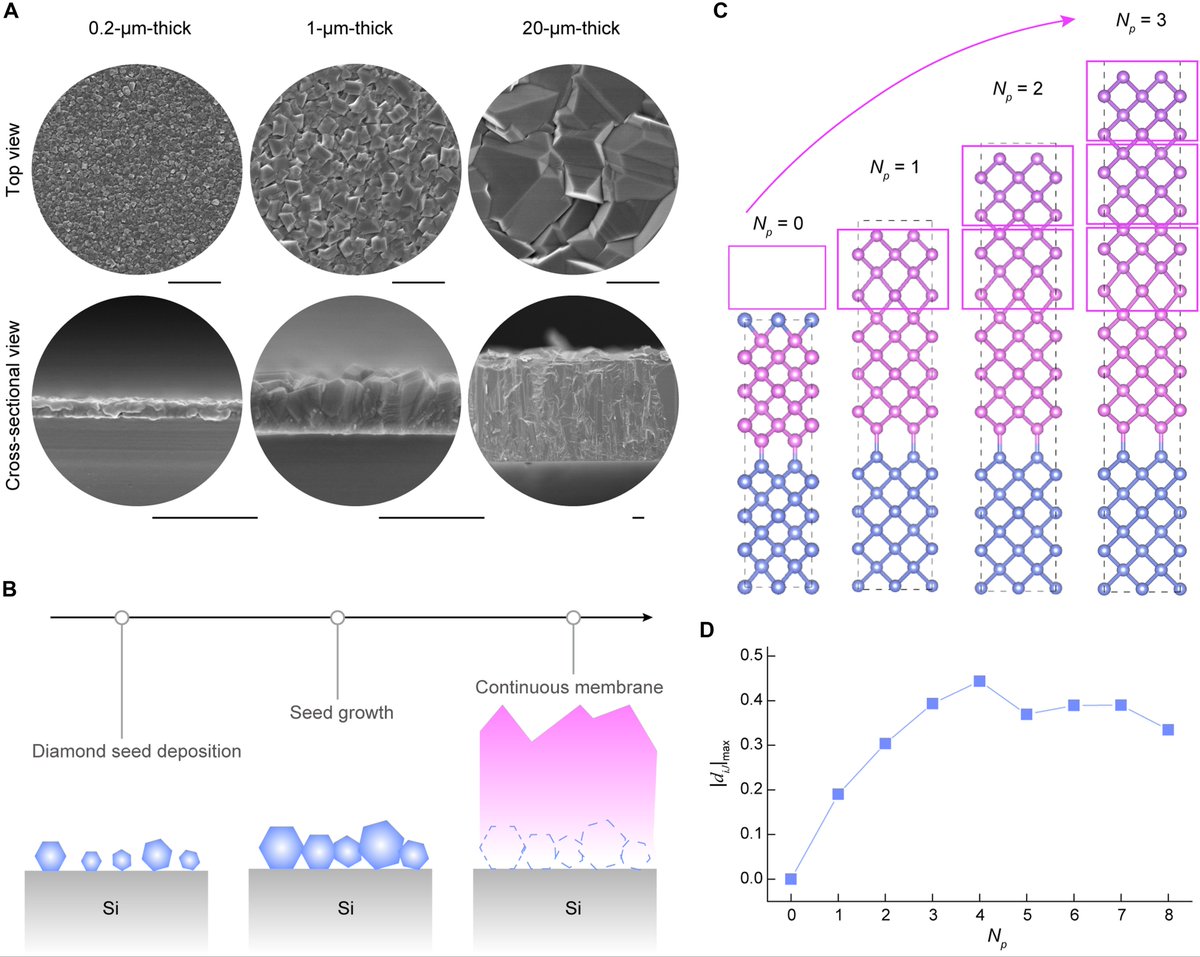
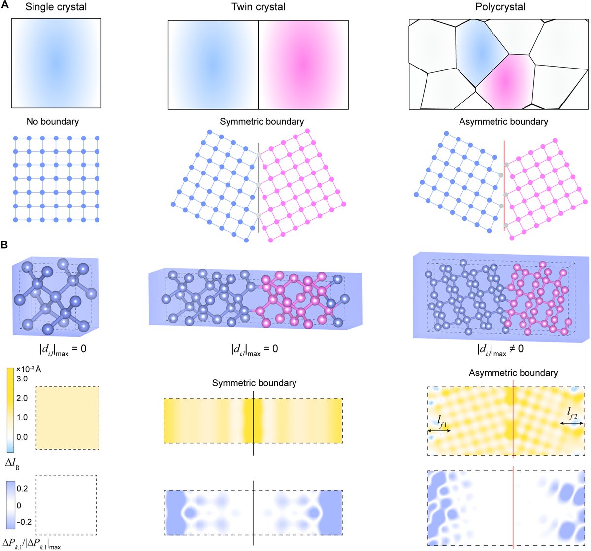
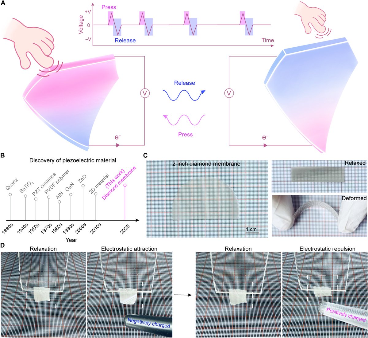
Diamond just learned to generate electricity, rewriting a century of materials science dogma. Ultrathin polycrystalline diamond membranes flex and produce stable voltage under bending, with peak piezoelectric performance rivaling or surpassing conventional materials, all thanks to grain boundary asymmetries unlocked by edge-exfoliation fabrication.
A material once relegated to passive substrates now actively generates power from motion. Expect rapid follow-ons in diamond-based piezo devices; this reopens textbooks and accelerates applications leveraging diamond’s legendary resilience.
HKU breakthrough shatters the long-held view that perfect diamond’s centrosymmetric crystal structure forbids piezoelectricity. Single-crystal or twin diamonds stay inert, but polycrystalline versions – engineered ultra-flexible and thin (~5 μm optimal)– accumulate charge polarization at asymmetric grain boundaries during deformation, creating measurable potential differences across the membrane.
Voltage coefficient hits ~82.2 mV·m/N at peak thickness; durable through thousands of bending cycles with negligible degradation, ruling out artifacts via rigorous controls. Diamond’s unmatched traits (biocompatibility, chemical inertness, thermal conductivity, hardness, wide bandgap) now pair with self-powering and sensing capabilities.
The team’s edge-exfoliation innovation bends the unbreakable, proving polycrystalline quirks can birth revolutionary properties absent in pristine forms. Deformation amplifies local asymmetries at boundaries, polarizing charges without violating symmetry in bulk.
1
1
77

Jun 12
Industry Overview (Current Trends & Company’s Position)
India is currently undergoing an unprecedented green revolution, aiming to secure $500\text{GW}$ of renewable energy capacity by 2030. Within this framework, two critical policy initiatives are driving secular growth:
PM-Surya Ghar: Muft Bijli Yojana: Targeting 1 Crore (10 million) households with subsidized rooftop solar, creating a massive addressable retail market.
PM-KUSUM Scheme: Empowering rural farmers by replacing diesel water pumps with solar-powered pumps.
APSIL is strategically positioned. It is an Approved List of Models and Manufacturers (ALMM) registered manufacturer with the Government of India, making its panels eligible for federally subsidized projects.
By transitioning from polycrystalline modules to high-efficiency N-Type TOPCon panels, APSIL remains globally competitive against cheap Chinese imports while retaining domestic manufacturing incentives.
(7/25)
1
54
Jun 12
Products & Services Portfolio
The company’s diverse product and service ecosystem addresses multiple segments of the clean energy market:
A. Hardware Products
Solar PV Modules: Ranging from 10W to over 450W . Product lines include:
N-Type TOPCon Modules (Max Series): Advanced high-efficiency modules representing the latest market technology.
P-Type Mono Bifacial & Monofacial Modules: High yield, optimized for Indian climatic conditions.
Polycrystalline Modules: For cost-sensitive applications.
Grid-Tied Solar Inverters: Ranging from 1W to 110W in single-phase and three-phase options, equipped with GPRS/WiFi monitoring.
Solar Water Pumps: Both AC and DC high-efficiency pumps optimized with MPPT (Maximum Power Point Tracking) technology for irrigation.
B. Technical Services
Site Auditing & System Design: Custom layout creation optimized for maximum solar radiation.
Turnkey Installation: Quick-deployment mounting structures built with corrosion-resistant galvanized iron.
Operations & Maintenance (O&M): Annual maintenance contracts (AMC), cleaning, and performance optimization services.
(4/25)
1
65
Jun 12
Business Model (How the Company Makes Money)
APSIL operates a vertically integrated business model that spans manufacturing and service integration. Instead of relying solely on low-margin component sales, APSIL captures margins at multiple points of the solar value chain.
The company generates revenues from two principal business activities:
Manufacturing and Sale of Solar PV Modules: Delivering high-quality Monocrystalline, Polycrystalline, and advanced N-Type TOPCon panels to distributors, system integrators, and project developers.
EPC (Engineering, Procurement, and Construction) Services: Offering end-to-end turnkey solutions. This includes engineering design, site procurement, installation, and commissioning of rooftop solar plants for residential, commercial, and industrial (C&I) clients, as well as agricultural solar water pumping systems under government subsidies.
By manufacturing its own panels, APSIL keeps its raw material costs for its EPC projects highly competitive.
(3/25)
1
62

Jun 12
🔥 WANG SOLAR 🔥
*200W Supersun Floodlight*
🔻Battery:LiFePO4 18000mAh
🔻Solar pannel:A-level polycrystalline silicon 5V/25W (430*350mm)
🔻 Charging Time:6-8HRS
🔻Discharge time:18 hours
🔻Install height:4-6M
🔻Irradiation area:150 square
7000
Call:0743814879

21

Jun 11
A Scalable Fishbone Nanowire Array (FINE) for 3D Quasi-Intracellular Recording in Intact Brains
A Fishbone Intracellular Nanowire Electrode (FINE) is developed with ultra-sharp nanowire tips strategically integrated at slanted angles along an implantable shank to record 3D intracellular potentials from ensembles of neurons in intact brain.
A novel fabrication process is developed to integrate reverse-angled polycrystalline platinum silicide (PtSi) nanowires to preserve the structural integrity of FINE during insertion. As-implanted or sub-micron retraced FINE spreads the polycrystalline platinum silicide (PtSi) nanowires away from the shank to establish intimate nanowire-neuron interfaces that yield quasi-intracellular potentials. Comparative analyses of nanowire recordings versus adjacent planar recordings on the same shank validate their distinctive quasi-intracellular recording characteristics.
The scalability of FINE is demonstrated to a 3D 24-shank array with 594 nanowires and 430 planar contacts and successfully identified quasi-intracellular potentials across 127 distinct nanowires in the intact brain. FINE's 3D quasi-intracellular recording holds the potential to unlock detailed investigations of the intricate ionic potential fluctuations and patterns of transmembrane potentials that drive behavior and cognition.
iebl.ucsd.edu/sites/default/…


2
12
33
2,034