no retweeted

CoPoSに関して情報が錯綜しているポヨね
ガラスの先端パッケージングへの用途は3種類あるポヨ
1.最終的には取り外す土台となるキャリア
2.ビルドアップ基板のコア用
3.インターポーザ用
TSMSはまずは生産性のため、RDLインターポーザのキャリア用としてガラスを使うポヨ
2番のコア用は少し先の話ポヨ
Jun 11

⚙️TSMCのCoPoS、量産は2028年後半へ | AI大型パッケージの制約はガラスより実装歩留まりにある $TSM $NVDA
TSMC $TSM の次世代先端パッケージ CoPoS が、AI半導体の制約がどこへ移るかを少し先回りで示している。6月11日にMing-Chi Kuoがまとめた内容では、CoPoS の量産は2028年後半を想定し、9.5倍レチクル級を超える超大型パッケージの経済性改善が狙いになる。初期採用候補として名前が挙がるのは NVIDIA $NVDA の Feynman だ。
この話が効いてくるのは、AIインフラの勝負がプロセスノードだけでは完結しなくなっているからだ。TrendForce は4月13日、Commercial Times を引用し、CoPoS のパイロットラインが6月完工に向かい、量産立ち上がりは2028〜29年と報じた。背景にあるのは、GPUのレチクルサイズ拡大で12インチウエハー当たりの取り数が落ち、従来の丸いウエハー前提では利用効率とスループットが厳しくなるという問題である。
ここで誤読しやすいのが、CoPoS を単純なガラスインターポーザの話として受け取ることだ。Kuoの説明では、ガラスは一時キャリアとガラスコア基板側に使われ、インターコネクトの役割はチップ側RDL、TGV/Cu、ABF積層が担う。つまり投資家が追うべき論点は、ガラスという材料名そのものではない。超大型基板で反りと歩留まりを抑えながら量産できるか。その一点に近い。
AIインフラのボトルネックはこれまで、先端ロジック、HBM、CoWoS容量の順に語られてきた。CoPoS が本当に2028年後半へ滑り込むなら、その次はパッケージ面積と実装コストが制約になる。Kuoはこの技術が2032年ごろまで TSMC の先端パッケージ優位を補強するとみている。話を単純化すれば、NVIDIAのような最先端顧客が、より大きい計算資源を一枚のパッケージに載せ続けるための器を、TSMCが先に用意できるかどうかだ。
まだ量産まで2年以上ある。株価材料としては早い。ただ、制約の位置は早めに見えてくる。Feynman世代の実装方式、CoPoS のパイロット進捗、そして反りと歩留まりに関する追加開示。この3点が、2027年以降のAIサプライチェーンで誰が交渉力を持つかを決め始める。
🤘情報提供
Stock Slayer : stock-slayer.com/?p=post-202…
6
66
13,424

Jun 11
If everything just works… that’s usually not an accident.
Roundtable TSMS 12.8.2 is here—focused on OpenEdge compatibility, security alignment, and a few targeted fixes (XREF, Change Finder, Blame View). No new features—just smoother workflows.
👉 roundtable-software.com/supp…
12

Jun 10
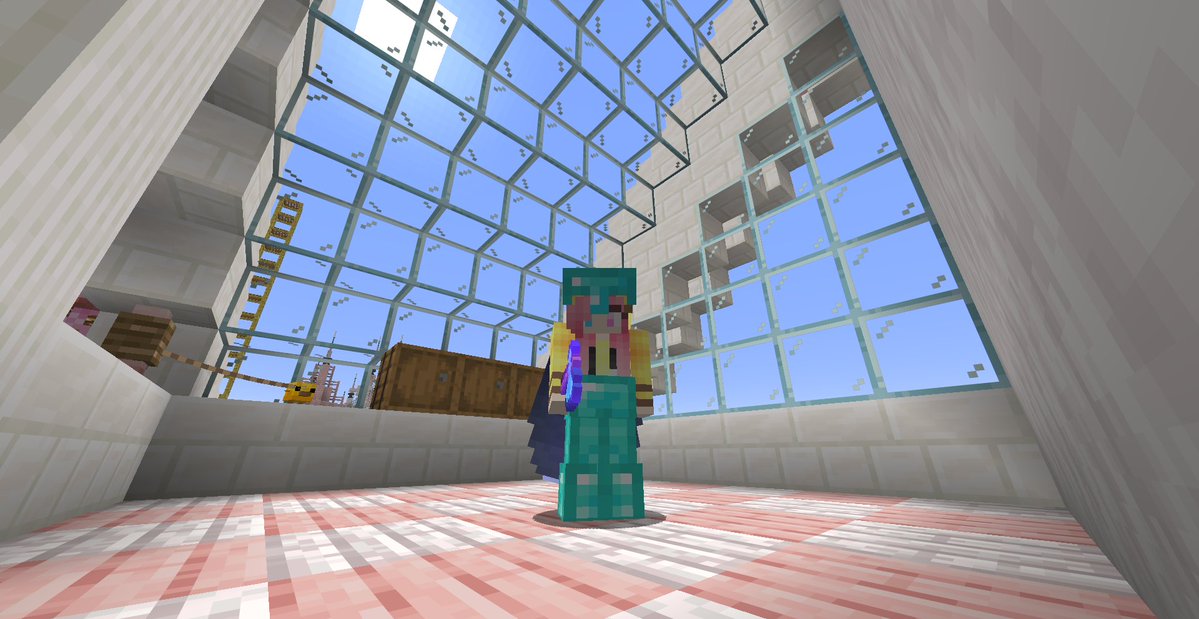
【#TSMS鯖】
オプティファインのプレ版が出たので、早速、シェーダーを入れて見てみた😍
そして、相変わらず建築途中のちえぴょん拠点を見回ってみた😋
いつも通り、倉庫だけはしっかりと作る私でありました
🤭
変な所だけ几帳面で、細かくしまえる場所がないと嫌な人🤭
#Minecraft
#マイクラ
1
19
299

Nobody can beyond TSMS. Let's verify it in 2 years.

Elon Musk is essentially saying that, if his claim holds true, Tesla’s upcoming AI6 chip may extract an unusually high amount of working AI computing power from each silicon wafer 🔥
Here is exactly what it means in plain English 🧵
BREAKING DOWN THE JARGON
💿 Wafer: Computer chips aren't manufactured one by one. They are printed by the dozens or hundreds onto a giant, shiny, pizza-sized disc of silicon called a "wafer." Once the intricate printing process is done, this wafer is sliced up into individual square chips.
🏭 Yield: When you manufacture chips on a silicon wafer, not all of them come out usable. A microscopic speck of dust or a tiny printing flaw can damage a chip. "Yield" is the percentage of chips on the wafer that work well enough to be used. Sometimes a chip with a small flaw can still be used by disabling the damaged part or running it at a lower performance level.
🧠 Usable intelligence: This is Elon's phrase, not a standard chip-industry metric. He likely means useful AI processing power: how much real neural-network work Tesla can get from the chips that actually work. It is not "intelligence" in the human sense.
CONNECTING THE PIECES
Think of a silicon wafer like a large baking sheet, and the individual chips as cookies being baked on that sheet.
🍪 Every chip design tries to pack as many transistors—the brain cells of a chip—into a given area as possible to maximize computing power. However, silicon manufacturing is incredibly delicate.
📉 Imagine that every time you bake, a few random drops of liquid soap fall onto the baking sheet. If a drop lands on a cookie, that cookie is ruined. This is the reality of manufacturing defects.
🎯 This creates a massive trade-off problem. A bigger chip hurts you twice: fewer of them fit on each wafer, and each one is a bigger target with a higher chance of being ruined by a random defect. If you make the chips very small, more of them fit on the wafer and yield may improve, but each chip may not have enough computing power for serious AI workloads.
HOW TESLA MIGHT PULL THIS OFF
No one outside Tesla knows the exact AI6 design yet, so this part is best understood as an educated guess.
To maximize real neural-network work from each wafer, Tesla would likely need to optimize several things at once:
1️⃣ First, the chip must be the right size. Public reporting suggests AI5 is not a maximum-size chip, but closer to a more practical size that still leaves room for strong performance. That matters because a chip that is too large may be powerful, but fewer fit on each wafer and each one has a higher chance of being ruined by defects.
2️⃣ Second, the chip can be specialized for Tesla’s own AI workloads instead of being a general-purpose processor. If the hardware is designed mainly around the kinds of neural networks Tesla actually runs in cars, robots, and data centers, more of the silicon can be spent on useful AI work.
3️⃣ Third, Tesla may be able to improve yield by designing in redundancy, meaning a chip with a small defect could still be salvaged and used instead of being thrown away. This is common in advanced chip design, though we do not know the exact AI6 approach.
4️⃣ Fourth, memory bandwidth and power efficiency matter immensely. Public AI5 details suggest Tesla is paying close attention to feeding data quickly into the chip. That is important because an AI chip is only useful if it can keep its AI engines busy without wasting too much energy.
So the achievement would not come from one magic trick. It would come from balancing chip size, specialization, memory, power, and manufacturability better than competitors.
THE BOTTOM LINE
The key point is that Elon’s claim is not just about making the most powerful individual chip. It is about maximizing the total amount of useful AI compute Tesla gets from each wafer.
The rough equation is:
Usable AI compute per wafer = how many chips fit on the wafer × how many survive manufacturing × how powerful each working chip is
So when Elon says AI6 might set a record for "the most amount of usable intelligence from a wafer when factoring in yield," he is saying Tesla may have optimized the whole system: chip size, defect tolerance, AI specialization, memory, power efficiency, and manufacturing yield.
In plain English, the win would not simply be:
"We made a giant chip".
It would be:
"We got the most working AI brainpower out of each expensive silicon wafer".
That is why the yield part matters. A chip only counts if it actually works, and the real engineering achievement is maximizing the amount of useful AI work that survives the manufacturing process.

47

Jun 10
People don't get that TSMs CPO delay to 2029 because of FAU problems is actually great for the TSEM NPO fix. see you at earnings 📉
94

きょうのTSMS月次は十分強いともうわかってる感ありそうだけども、前工程強いのもそういうこと??
Taiwan May exports hit second-highest value by month on strong AI demand reuters.com/world/asia-pacif…
1
1
16
6,453
Jun 8

17
171


Jun 5
休肝日から無事生還のハナトーラ…
今日はこのコから🎵😆
TSMS A Lowland Distillery 2007 15 48%
HB で
ウン❗キ◯ンチーデス🎵もう一度言う…キ◯ンチーデス🎵KP 😄👍

58
251
May 31
6
73
这是EUV受限前提下的创新。另辟蹊径,追赶TSMS。畅想一下,2030后, EUV突破,韬尔定律生效,华为系的竞争力会有多强。
1
2
211
May 28
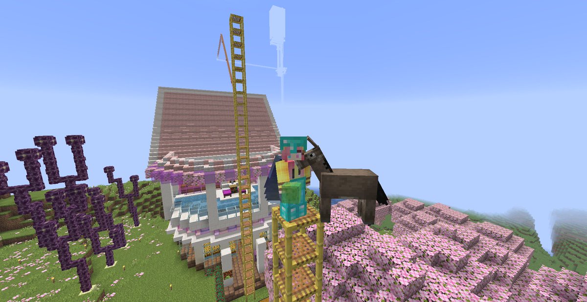
【#TSMS鯖】
久しぶりに、遊べた☺️⛏
足場を上って、上から見ようと思ったら、影があって、団長がいるのかと思ったら、ロバだった🫢
足場上るのね🫢
そして、村人の治療が進んだ☺️
そして、まだ拠点が完成しない🤫
#Minecraft
#マイクラ

1
1
16
138
May 24
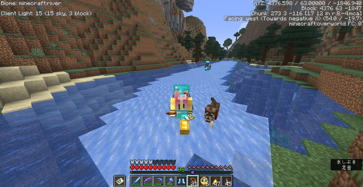
【#TSMS鯖】
体調が落ち着いて、マイクラログイン☺️⛏
オオカミ探しに行ったり、くろねこ捕まえたり、久しぶりに遊べた😋✨
現在、ハニカム収穫機も作りたくて、作業中🐝
#Minecraft
#マイクラ
1
1
14
98

May 23
ライトハウス続き
・TSMS バーギー
・よくわかんないトーモア(酔
トーモアはラベルの雰囲気と美味すぎで一瞬オールドかと思ったけど違った、ごちそうさまでした😋


10
237