
🚨 #BREAKING: Applied Materials $AMAT Introduced Two New Chipmaking Systems Designed to Solve One of the Biggest Challenges in Advanced Semiconductor Manufacturing.
What was announced:
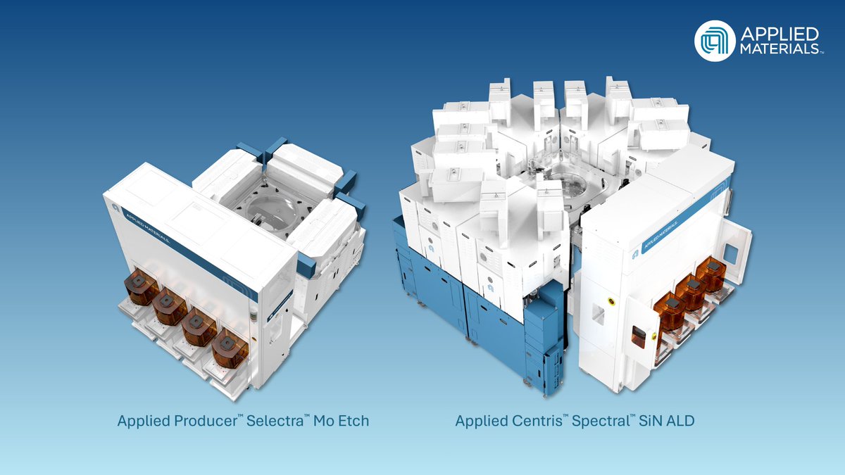
➜ Applied Materials $AMAT introduced two new systems: the Centris Spectral SiN ALD and the Producer Selectra Mo Etch.
➜ Both systems were announced alongside the 2026 IEEE Symposium on VLSI Technology and Circuits.
The problem they solve:
➜ Modern AI chips increasingly rely on stacking structures vertically rather than simply shrinking them horizontally.
➜ As these structures become deeper and narrower, it becomes much harder to coat materials evenly or remove materials precisely throughout the entire structure.
➜ Existing manufacturing tools are increasingly challenged by these requirements.
➜ Variability in these processes can reduce electrical performance and lower manufacturing yields.
➜ Both new systems are designed to address this challenge from different angles.
Centris Spectral SiN ALD:
➜ Silicon nitride is a key insulating material used throughout the chip manufacturing process.
➜ It is used for surface protection, electrical isolation, and as a spacer during patterning.
➜ The material must be deposited at low temperatures while remaining durable enough to withstand later manufacturing steps.
➜ Conventional plasma-enhanced deposition struggles to uniformly coat high-aspect-ratio structures.
➜ The Centris Spectral SiN ALD uses high-density microwave plasma technology to deposit high-quality silicon nitride uniformly inside tall, narrow structures.
➜ The system is designed to achieve this at low temperatures while avoiding the tradeoff between plasma density and ion-induced damage.
➜ In gate-all-around transistors, the system can create high-quality liners for transistor contacts that reduce electrical resistance and capacitance.
➜ Lower resistance and capacitance can enable faster device performance.
➜ Applications extend across advanced logic and DRAM manufacturing.
➜ The system is part of Applied Materials' new Spectral ALD platform.
➜ The platform features a quad-reactor design, precision chemical delivery, and support for both temporal and spatial ALD operation.
➜ Applied Materials said the system is being adopted by leading chipmakers.
Producer Selectra Mo Etch:
➜ 3D NAND memory chips store data by stacking memory cells vertically, often across hundreds of layers.
➜ Molybdenum is increasingly being used for the wordlines that connect those memory cells.
➜ To prevent electrical shorts, the metal must be removed precisely from the spaces between adjacent wordlines.
➜ Conventional wet etch processes struggle to remove material evenly throughout the full depth of these structures.
➜ The Producer Selectra Mo Etch uses an engineered dry gas process to achieve uniform top-to-bottom molybdenum removal across the full stack.
➜ Applied Materials said the system has already been validated in high-volume manufacturing.
➜ The system reduces cell-to-cell variability.
➜ It lowers leakage current.
➜ It improves data retention.
➜ Applied Materials also said the technology creates opportunities beyond 3D NAND, including DRAM and foundry logic applications.
What Applied Materials says:
➜ Dr. Prabu Raja, President of the Semiconductor Products Group at Applied Materials, stated: "As the industry pushes the limits of AI computing, the biggest opportunities are increasingly found in materials engineering. From transistor structures to memory stacks, chipmakers need new ways to precisely deposit and selectively remove materials in extremely complex 3D architectures."

6


Chipmaking giant Nvidia Corp. is looking to sell at least $20 billion of bonds on Monday, joining a wave of companies that are borrowing as they pay for investments in the artificial intelligence boom. eastbaytimes.com/2026/06/15/…
1
117

Chipmaking giant Nvidia is set to raise $25 billion from a high-grade bond sale that received more than 3️⃣ times that amount in demand, underscoring relentless investor appetite for exposure to the artificial intelligence boom

1
39
Gonzalo torres retweeted

$AMAT rolled out two new chipmaking systems to help manufacturers build advanced 3D chip structures as the industry pushes for more density.
Applied Materials says the tools are designed to solve key manufacturing bottlenecks tied to stacked transistor designs.

1
4
329

This is why the future will be won by NOT outsourcing manufacturing and ensuring that you are not training potential rivals in your universities or hiring them to train them in corporations that deal in professional manufacturing, chipmaking, drone-making, refining etc.
1
2
89
Beastwood retweeted

Applied Materials $AMAT introduces two new chipmaking systems for advanced 3D structures.
1
14
4,935
Bill W retweeted

$AMAT rolled out two chipmaking systems for 3D structure production as the industry pushes density gains.
Applied Materials positioned the tools to solve manufacturing constraints tied to stacked transistor designs.
1
1
5
1,088

The surge in AI compute is accelerating the industry’s transition to advanced 3D device architectures, including gate-all-around (GAA) transistors and high-layer-count 3D NAND. To address this emerging challenge, we're introducing two new chipmaking systems designed to achieve precision processing in increasingly deep and narrow 3D structures.
Together, the new Centris™ Spectral™ SiN ALD* and Producer™ Selectra™ Mo Etch provide chipmakers with precise control over both dielectric film deposition and metal removal in high-aspect-ratio structures. The result is more uniform materials engineering at advanced nodes, enabling continued 3D scaling with better device performance, tighter process control and improved manufacturability across logic and memory applications.
Learn More: bit.ly/4xvZo9o
13
864

$AMAT | Applied Materials Unveils New AI Chip Manufacturing Systems
Key Points:
Applied Materials launches two new systems for advanced 3D semiconductor manufacturing
New tools target processing challenges in high-aspect-ratio AI chip structures
Centris Spectral SiN ALD enables highly uniform silicon nitride deposition in deep 3D features
Uses advanced microwave plasma technology for low-temperature, high-quality film formation
Supports next-generation GAA transistors, DRAM, and advanced logic chips
Producer Selectra Mo Etch enables selective molybdenum removal for advanced 3D NAND production
Improves wordline separation, reducing defects, leakage, and variability
Enhances manufacturing yield, performance, and energy efficiency for AI chips
Technologies are already being adopted by leading logic and memory semiconductor manufacturers
Takeaway:
The launch strengthens Applied Materials' position in the AI semiconductor equipment market, addressing critical manufacturing bottlenecks as chipmakers move toward more complex 3D architectures.
#AMAT #AppliedMaterials #AI #Semiconductors #Chipmaking #DRAM #3DNAND #GAA #DataCenter
37

Tim Cook named advanced chip supply Apple's greatest supply chain constraint — Intel just became the escape hatch. 🔧
The Intel deal is preliminary but real, aimed at future chip capacity. Intel's foundry arm isn't expected to turn profitable until 2028, but Apple volume would move that clock: a real customer turns a turnaround slide into factory proof. Samsung talks are exploratory, no orders placed, non-TSMC supply risk unresolved.
The real stress test is Intel's 18A node, a chipmaking recipe still needing mass production proof. This isn't an Intel comeback story — it's Apple engineering its own supply-chain leverage.
#Samsung #Semiconductors #TSMC #SupplyChain #JudithAICast #AI #Markets #Tech
1
26

Trump’s deal to assume a 10 percent stake in chipmaking giant Intel breaks with years of U.S. economic precedent. But from a global perspective, parts of the deal appear much more ordinary. washingtonpost.com/world/202…
7

Nvidia Corp. has received about $85 billion of orders for its jumbo debt offering, underscoring relentless investor appetite for exposure to financing tied to the artificial intelligence boom.
The chipmaking giant is seeking to raise at least $20 billion from a bond sale on Monday, while the size of the offering could still be boosted, according to people with knowledge of the matter. Demand exceeded four times that minimum amount at its peak, one of the people said, asking not to be identified because they aren’t authorized to speak publicly.

1
19

Advanced chipmaking demand fueled $ASML 👀🔥
$514K came through and price reacted instantly.
It climbed to $2,316.94, bringing the position to $1,899,426 🤯
That’s a 391% move 🚀⚡
Momentum remains intact.


1
128

Chipmaking giant Nvidia Corp. is looking to sell at least $20 billion of bonds on Monday, joining a wave of companies that are borrowing as they pay for investments in the artificial intelligence boom. mercurynews.com/2026/06/15/n…
1
26

Less is Moore: China's chipmaking capacity is formidable, but it still lags the US on the hardware and software frontier ⬇️
pantheoninsights.substack.co…
9
