
Jun 16
Scan disk
Microtechnologies
Nvidia
Now SpaceX.
I guarantee this is going to be the fourth year in a row that my portfolio has outperform S&P.
Life is good I just wish I would have started this shit 40 years ago
1
2
359

May 11
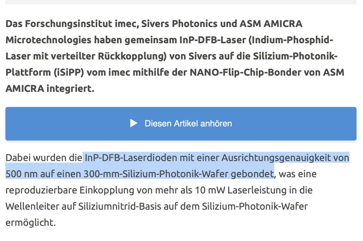
$SIVE Photonics & @imec_int - The Silent Enabler Behind Photonic Quantum Computing and Next-Gen AI Infrastructure
Sivers Photonics has quietly become one of the most strategically important players in the race for scalable silicon photonics, and the latest milestone with imec proves it.
Together with imec (the world-leading independent nanoelectronics and digital-tech research institute in Leuven) and ASM AMICRA Microtechnologies, Sivers has successfully integrated its high-performance InP-DFB lasers (Indium-Phosphide) onto imec’s iSiPP silicon-photonics platform.
Using ASM AMICRA’s ultra-precise NANO-Flip-Chip-Bonder, the InP laser diodes were bonded onto 300mm silicon-photonics wafers with an alignment accuracy of <500 nm. The result: repeatable optical coupling of more than 10 mW of laser power into the silicon-nitride waveguides, a critical breakthrough for commercial-scale photonic systems.Why this mattersSilicon itself cannot generate light.
Every photonic chip, whether for AI accelerators, optical interconnects, or fault-tolerant quantum computers, needs external laser light sources.
Sivers’ hybrid integration on 300mm wafers (the semiconductor industry standard) solves exactly that problem at scale.
Industrial scalability unlocked: Sivers moves from lab to mass production. Its InP100 platform now delivers laser arrays perfectly matched to imec’s wafer designs.
Industry-standard validation: By becoming a core building block in imec’s iSiPP platform and Process Design Kits (PDKs), Sivers’ technology is automatically available to any chip designer using imec’s services, from hyperscalers to telecom giants.
Lock-in effect: Once a design (e.g., a new $CSCO switch or $MRVL/ $AVGO transceiver) is validated on a Sivers-based PDK, swapping the laser supplier becomes extremely expensive and time-consuming.
The ecosystem impact is massive
@PsiQuantum already relies on Sivers’ lasers for its photonic quantum computer (currently scaling in Chicago).
$NVDA, $INTC, $GOOG, $MSFT & $AMZN all use imec’s prototyping services for 2028 roadmaps. Co-Packaged Optics (CPO) and optical I/O are non-negotiable for them, exactly the use case Sivers now dominates.
Strategic partners: $ASML (lithography), ASM AMICRA (bonding), and $GFS (foundry) are directly in the workflow.
Additional tailwinds: $JBL: Joint development of 1.6T LRO transceiver modules (April 2026 announcement, landing Sivers directly into the racks of the world’s largest cloud providers.
$AAPL: Long-running speculation around optical sensing (health/biometrics) using Sivers’ precision InP lasers.
$NOK & Ericsson: Tier-1 telecom infrastructure partnership for next-gen 5G/6G beamforming chips.
$AMZN & $META Their custom ASICs (Trainium/Inferentia, MTIA) need optical interconnects, and Ayar Labs (Sivers partner) already points straight to Sivers’ validated light sources.
6
8
103
8,740

Apr 29
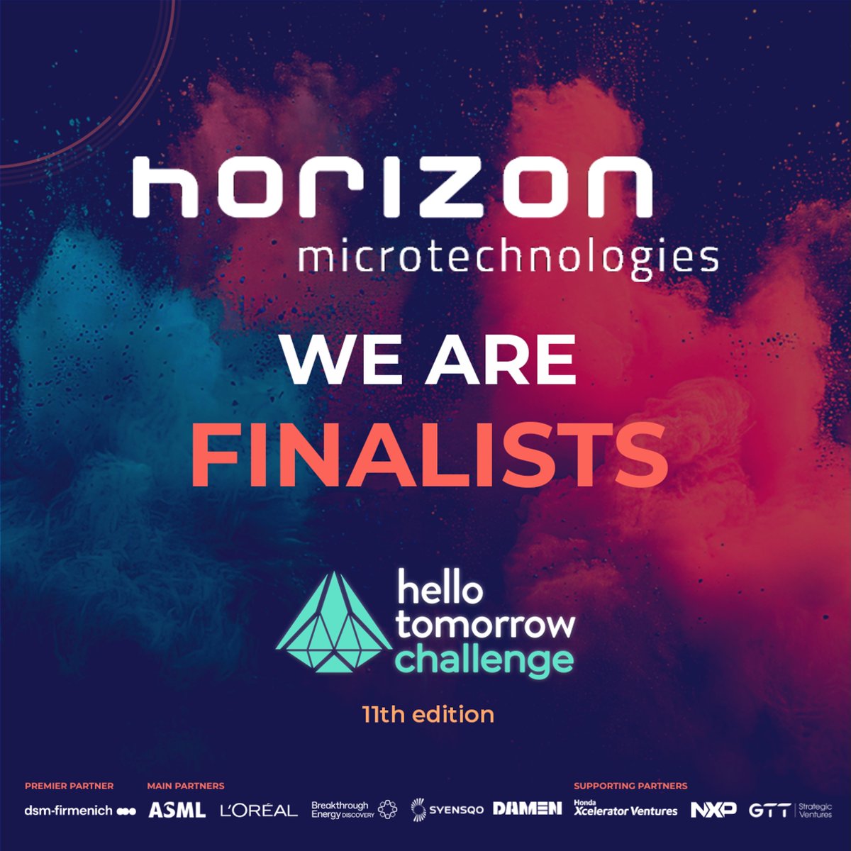
HORIZON MICROTECHNOLOGIES NAMED HELLO TOMORROW FINALIST IN AEROSPACE TRACK, STRENGTHENING MOMENTUM AHEAD OF MAJOR INVESTOR PITCH CYCLE
engineering-update.co.uk/202…
1
2
45

Apr 28
Horizon Microtechnologies has been selected as a finalist in the Hello Tomorrow Global Challenge – Aerospace track, securing the opportunity to pitch for the €100,000 Grand Prize.
eurekamagazine.co.uk/content…
#DeepTechInnovation #AerospaceStartups #HelloTomorrow
2
34

Mar 23
By combining micro-scale #3Dprinting by Boston Micro Fabrication @bmf3d with advanced coatings, Horizon Microtechnologies is targeting applications like electronics packaging, space components, and antennas. Now, it is delving deeper into another application: microfluidics. @pilz
Mar 23

Horizon Microtechnologies Expands Into Microfluidics dlvr.it/TRfHKz
2
5
166
Mar 20
HORIZON MICROTECHNOLOGIES COMBINES MICRO-AM WITH ADVANCED COATINGS FOR FUNCTIONALISED 3D MICROFLUIDIC DEVICES - engineering-update.co.uk/202…

1
1
2
67

Ichthyophagous
Immunocytochemically
Immunofluorescence
Immunohistochemistry
Immunomodulatory
Immunopathologically
Incompatibilities
Incomprehensibleness
Indistinguishability
Industrialization
Infectiological
Infraspinatus
Infratentorial
Inhomogeneities
Insurmountabilities
Interchangeabilities
Intercontinental
Interdepartmental
Interdenominational
Interdisciplinarily
Interferometrically
Interinstitutional
Interleukinopathies
Internationalization
Interoperabilities
Interpersonalization
Interproximities
Interrelationship
Intersegmental
Intracerebroventricular
Intracoronary
Intralinguistically
Intramuscularly
Intragastrically
Intraocular
Intraoperatively
Intraspecific
Intravenously
Introductory
Ionophoretically
Irresponsibilities
Isobarometrically
Isothermalization
Isozymatically
Kaleidoscopically
Karyologically
Kinesiotherapeutically
Laboratorially
Lexicographically
Linguistically
Lithographically
Magnetoelectrically
Magnetophotography
Malacostracologically
Maladministration
Mammographically
Manoeuvrabilities
Manuscripturally
Mathematician
Mechanochemically
Mechanographically
Metallographically
Metaphysically
Metaphysiologically
Microanalytically
Microarchitectural
Microbiologically
Microelectrophoresis
Microencapsulation
Microphotometrically
Microprogrammable
Microspectrophotometry
Microtechnologies
Microvasculature
Monochromator
Monosyllabically
Multifunctionalities
Multigenerational
Multihierarchical
Multimolecular
Multinucleated
Multiplicatively
Musculocutaneous
Myelencephalitis
Myocardiectomies
Nanostructurally
Neuroanatomically
Neurobiologically
Neuroendocrinology
Neuroepidemiologically
Neurofibrillary
Neurophysiologically
Neuroscientifically
Neurotransmissions
3
12
2,113

10 Dec 2025
#Microscopy, #fluorescence imaging and #OCT are transforming how we study cells in real time. EPIC Members like @coolLEDltd, IMT Microtechnologies, Opto GmbH, Wasatch Photonics and SERINO tech are paving the way. Read more at @Photoniques_edp
photoniques.com/articles/pho…
2
96

6 Dec 2025
We’re in a global technology race for microtechnologies and energy production, and your proposed net positive is cheap labor that Americans don’t want to do?
You better hurry and get back to work before you overcook someone’s Wendy’s order.
1
2
39

15 Nov 2025
Welcome to Kyptec LifeStyle
🎧 Born in India, for India and the world — “Kyptec® LifeStyle” represents the voice of a new generation that lives through sound, music, and connection. At “Kyptec® LifeStyle”, we fuse cutting-edge audio engineering with fashion-forward design, so whether you’re in the gym, on a call, in the studio, or deep into a late-night game, your gear always matches your mood. 💥 From noise cancelling headphones for total focus to noise canceling earbuds that charge in a flash, we’ve got your sound locked in. 🔒🎶
Designed in India, our audio gear is built for those who demand deep bass, crisp clarity, and all-day comfort — without compromising on style or budget.
Our Vision is to empower the youth with sound that reflects their passion, power, and personality — making advanced audio technology accessible, relatable, and proudly Indian.
KYPTEC® Lifestyle is not just an audio brand — it’s a global lifestyle movement born in India and built for the world.
A registered trademark owned by BalaJi MicroTechnologies Pvt. Ltd. (A Unit of the B.B. Group of Companies), we proudly operate from our corporate headquarters in New Delhi, India.✨
“Kyptec® Lifestyle” is a homegrown Indian premium wireless audio brand founded by Mr. Nitin Aggarwal and Mrs. Sweta Aggarwal....🎧🔥
“Kyptec® LifeStyle” is a dynamic Indian brand redefining the audio experience for the Gen Z and Millennial generation. With a strong belief in innovation, self-expression, and high-quality engineering, we design and manufacture premium ear buds, headphone and earphones etc. that combine cutting-edge audio technology with bold, youthful aesthetics...🎵💫
🎮 Gamers:- lose yourself in crystal-clear sound with our gaming headset.
🎶 Music lovers:- dive into premium bass and ANC headphones that keep the noise out and the vibes in.
🏋️ On-the-go hustlers:- enjoy the freedom of wireless headphones and wireless earbuds built for all-day comfort.
Going Global 🌍🚀
Kyptec® LifeStyle is “Designed in India, Loved Worldwide.”
From our innovation hub in New Delhi, we are expanding rapidly into global markets — exporting to Asia, Europe, the Middle East, and North America.
🎯 Our ambition:
Build a multi-million USD turnover company within next 1~2 years, scaling into a $125M global audio powerhouse with exports, omnichannel retail, and disruptive growth strategies.
Compete with and out perform international audio giants.
Establish KYPTEC® as a global powerhouse in lifestyle audio technology.
Every export shipment, every new product launch, and every sales milestone is part of our mission to put India on the world audio map.🌍
🎧 Your Sound. Your Vibe. Your “Kyptec® LifeStyle...🚀🚀
Visit Corporate Website: kyptec-lifestyle.com
3
14

15 Nov 2025
Welcome to Kyptec LifeStyle
🎧 Born in India, for India and the world — “Kyptec® LifeStyle” represents the voice of a new generation that lives through sound, music, and connection. At “Kyptec® LifeStyle”, we fuse cutting-edge audio engineering with fashion-forward design, so whether you’re in the gym, on a call, in the studio, or deep into a late-night game, your gear always matches your mood. 💥 From noise cancelling headphones for total focus to noise canceling earbuds that charge in a flash, we’ve got your sound locked in. 🔒🎶
Designed in India, our audio gear is built for those who demand deep bass, crisp clarity, and all-day comfort — without compromising on style or budget.
Our Vision is to empower the youth with sound that reflects their passion, power, and personality — making advanced audio technology accessible, relatable, and proudly Indian.
KYPTEC® Lifestyle is not just an audio brand — it’s a global lifestyle movement born in India and built for the world. A registered trademark owned by BalaJi MicroTechnologies Pvt. Ltd. (A Unit of the B.B. Group of Companies), we proudly operate from our corporate headquarters in New Delhi, India.✨
“Kyptec® Lifestyle” is a homegrown Indian premium wireless audio brand founded by Mr. Nitin Aggarwal and Mrs. Sweta Aggarwal....🎧🔥
“Kyptec® LifeStyle” is a dynamic Indian brand redefining the audio experience for the Gen Z and Millennial generation. With a strong belief in innovation, self-expression, and high-quality engineering, we design and manufacture premium ear buds, headphone and earphones etc. that combine cutting-edge audio technology with bold, youthful aesthetics...🎵💫
🎮 Gamers:- lose yourself in crystal-clear sound with our gaming headset.
🎶 Music lovers:- dive into premium bass and ANC headphones that keep the noise out and the vibes in.
🏋️ On-the-go hustlers:- enjoy the freedom of wireless headphones and wireless earbuds built for all-day comfort.
Going Global 🌍🚀
Kyptec® LifeStyle is “Designed in India, Loved Worldwide.” From our innovation hub in New Delhi, we are expanding rapidly into global markets — exporting to Asia, Europe, the Middle East, and North America.
🎯 Our ambition:
Build a multi-million USD turnover company within next 1~2 years, scaling into a $125M global audio powerhouse with exports, omnichannel retail, and disruptive growth strategies.
Compete with and out perform international audio giants.
Establish KYPTEC® as a global powerhouse in lifestyle audio technology.
Every export shipment, every new product launch, and every sales milestone is part of our mission to put India on the world audio map.🌍
🎧 Your Sound. Your Vibe. Your “Kyptec® LifeStyle...🚀🚀
Visit Corporate Website: kyptec-lifestyle.com/
3
16

14 Nov 2025
Welcome to Kyptec LifeStyle
🎧 Born in India, for India and the world — “Kyptec® LifeStyle” represents the voice of a new generation that lives through sound, music, and connection. At “Kyptec® LifeStyle”, we fuse cutting-edge audio engineering with fashion-forward design, so whether you’re in the gym, on a call, in the studio, or deep into a late-night game, your gear always matches your mood. 💥 From noise cancelling headphones for total focus to noise canceling earbuds that charge in a flash, we’ve got your sound locked in. 🔒🎶
Designed in India, our audio gear is built for those who demand deep bass, crisp clarity, and all-day comfort — without compromising on style or budget.
Our Vision is to empower the youth with sound that reflects their passion, power, and personality — making advanced audio technology accessible, relatable, and proudly Indian.
KYPTEC® Lifestyle is not just an audio brand — it’s a global lifestyle movement born in India and built for the world.
A registered trademark owned by BalaJi MicroTechnologies Pvt. Ltd. (A Unit of the B.B. Group of Companies), we proudly operate from our corporate headquarters in New Delhi, India.✨
“Kyptec® Lifestyle” is a homegrown Indian premium wireless audio brand founded by Mr. Nitin Aggarwal and Mrs. Sweta Aggarwal....🎧🔥
“Kyptec® LifeStyle” is a dynamic Indian brand redefining the audio experience for the Gen Z and Millennial generation. With a strong belief in innovation, self-expression, and high-quality engineering, we design and manufacture premium ear buds, headphone and earphones etc. that combine cutting-edge audio technology with bold, youthful aesthetics...🎵💫
please visit website: kyptec-lifestyle.com/
3
19
29 Sep 2025
#3DPrinting News Briefs: Horizon Microtechnologies made system with solderability for metal-coated polymer #AM parts. @MELDMfg released DragonForge series. Modix large-format MAMA-1700 available. Kanfit acquired 2 @XJet_3d solutions. @uwanews Enactus Polymer to Purpose project.
27 Sep 2025
3D Printing News Briefs, September 27, 2025: Large-Format Pellet Printing, Recycled Polymers, & More dlvr.it/TNKTwt
2
481

12 Aug 2025
9:39, 12:34, 1-2-3-4, oh, you got me going didn't you.
12:34 is a time, specifically 12:34 PM (afternoon) or 12:34 AM (midnight). It can also be interpreted as a reference to 12:34 MicroTechnologies, a company specializing in IT solutions. Additionally, 1234 is considered an angel number, symbolizing new beginnings, personal growth, and trusting the journey, according to some interpretations of numerology.
Further Elaboration:
Time:.Opens in new tab12:34 can represent either 12:34 PM or 12:34 AM, depending on context. In a 24-hour format, it would be 12:34 for both PM and AM.
12:34 MicroTechnologies:.Opens in new tabThis company provides IT services and solutions. The brand name is derived from the time on a flip clock that a founder found annoying, but later embraced as a symbol of new beginnings and trusting the process.
Angel Number 1234:.Opens in new tabIn numerology, the number 1234 is often seen as an angel number. It signifies a journey of self-discovery, personal growth, and moving forward with confidence. It's a reminder to trust the path you're on and to embrace new opportunities.
Spiritual Significance:.Opens in new tab1234 is interpreted as a message to take control of your life, embrace independence, and strive for personal and spiritual fulfillment. It can also be a reminder to trust your intuition and inner guidance.🐈⬛🇺🇸🌠💫✨
1
2
21

1 Aug 2025
Horizon Microtechnologies has passed outgassing standard tests that bring us one step closer to using 3D printing components in space travel. tomshardware.com/3d-printing…
2
2
7
2,238

7 Jun 2025
A Review in @natrevbioeng discusses the recreation of key T cell interfaces using nanotechnologies and microtechnologies for the mechanistic study of T cell biology, as well as the manufacturing and sorting of T cell products. go.nature.com/4kVpUSp 🔒

6
19
13,484
16 May 2025
HORIZON MICROTECHNOLOGIES LAUNCHES RIGOROUS TESTING CAMPAIGN TO VALIDATE METAL-COATED 3D MICROFABRICATED POLYMER PARTS - engineering-update.co.uk/202…
1
2
34

17 Apr 2025
Horizon Microtechnologies announced that it has been working to validate the robustness of its micro #additivemanufacturing metal coating - metal-am.com/horizon-validat…
#3dprinting #manufacturing #engineering
2
64
3 Apr 2025
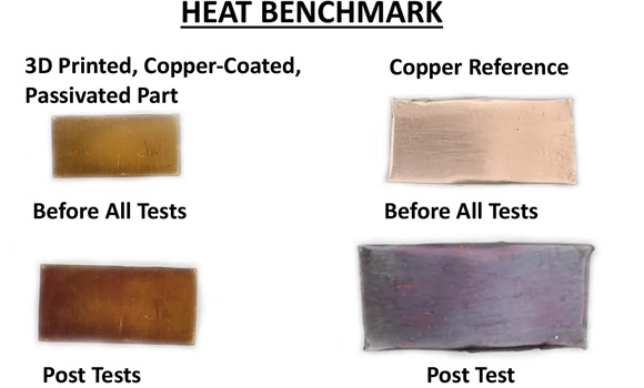
HORIZON MICROTECHNOLOGIES VALIDATES COPPER COATING DURABILITY WITH SUCCESSFUL PASSIVATION TESTING - engineering-update.co.uk/202…
2
62