
FYI in the latest dev build you can customize `outputPath` ✨
2
25


Mar 18
🚨SFN の落とし穴【障害調査ログ】
オッズ取得で一部が「締切後」になっていた問題が判明!
推定原因はこの2つ👇
📦 OutputPath による状態肥大化
→ 256KB制限で States.DataLimitExceeded
⚙️ INLINE Map の並列上限(40)
→ キュー待ちで trigger_at を通過
→ Waitスキップ
→ バースト実行
結果:締切後のオッズを取得していた可能性
🛠️ 対策(検証中)
・OutputPath: null
・DISTRIBUTED Map 化
・trigger_at スタガリング
💰 コスト増なしで改善予定
1
2
80

Mar 15
i'm looking for feedback, thank you
here's the full definition of my schematic:
import { mkdirSync, writeFileSync } from "node:fs"
import path from "node:path"
import {
defineCircuit,
definePart,
exportKiCadNetlist,
instantiate,
net,
pin,
} from "../../../tools/circuitd/src"
const ch32v203f8u6 = definePart({
id: "CH32V203F8U6",
kicadSymbol: "tinybee:CH32V203F8U6",
footprint: "tinybee:QFN-20_L3.0-W3.0-P0.40-BL-EP1.7",
defaultValue: "CH32V203F8U6",
datasheet: "ch32-riscv-ug.github.io/CH32…",
description: "144 MHz RISC-V MCU with ADCs, op-amps, advanced timers, and SWD",
fields: {
"LCSC Part": "C7570477",
},
designNotes: [
"Power this MCU from a 3.3 V rail only; do not allow the VDD pin to see more than 3.6 V.",
"Place a 100 nF decoupler immediately next to VDD and the QFN ground return, and keep that loop as short as possible.",
"Put a small series resistor between PA0 and any off-board throttle or one-wire configuration signal so the MCU pin is not directly exposed at the connector.",
"Keep PA13 and PA14 easy to probe and free of hard loads so SWD still works during bring-up and recovery.",
"Keep PA8, PA9, PA10, PA7, PB0, and PB1 on the three phase-drive nets, and keep PA6/BKI free for a future fault or protection input.",
"If you follow the openwch RISC-V ESC zero-cross scheme, tie PA3 and PA4 back into PA2 externally and reserve PA2 for that shared interrupt net.",
"Route back-EMF and op-amp related pins away from phase copper, gate-drive loops, and other fast-switching nodes.",
],
pins: {
"PA0/WKUP/ADC0": "1",
"PA1/ADC1": "2",
"PA2/ADC2/OP2O0": "3",
"PA3/ADC3/OP1O0": "4",
"PA4/ADC4/OP2O1": "5",
"PA5/ADC5/OP2N1": "6",
"PA7/ADC7/OP2P1/CH1N": "7",
"PB0/ADC8/OP1P1/CH2N": "8",
"PB1/ADC9/OP1O1/CH3N": "9",
"PB10/OP2N0": "10",
"PB11/OP1N0": "11",
"PB14/OP2P0": "12",
"PB15/OP1P0": "13",
"PA8/CH1": "14",
"PA9/CH2": "15",
"PA13/SWD/PA12/UDP": "16",
"PA14/SWC/PA11/UDM": "17",
"PA10/CH3": "18",
VDD: "19",
"PA6/ADC6/OP1N1/BKI": "20",
GND: "21",
},
})
const tlv75533pdqnt = definePart({
id: "TLV75533PDQNT",
kicadSymbol: "Regulator_Linear:TLV75533PDBV",
footprint: "tinybee:Texas_X2SON-4_1x1mm_P0.65mm",
defaultValue: "TLV75533PDQNT",
datasheet: "ti.com/lit/ds/symlink/tlv755…",
description: "500mA low-dropout fixed 3.3V regulator in 1x1mm X2SON-4",
designNotes: [
"Treat BATT as a 1S Li-ion or LiPo rail only; this regulator has a 5.5 V maximum input rating, so 2S or higher is out of bounds for this graph.",
"Place at least 1 uF ceramic directly at IN and at least 1 uF ceramic directly at OUT; do not push those capacitors away from the package.",
"Check regulator heating with (VIN - 3.3 V) * load current and add copper area if the dissipation is not comfortably safe.",
"Add local input bulk when the battery lead is long or inductive so the LDO input does not absorb line spikes by itself.",
"Keep EN tied to a known state at all times; if startup control matters later, break it out deliberately instead of bodging it in.",
"The X2SON thermal pad is internally tied to GND; flood it into the local ground copper and do not leave the center pad floating.",
],
pins: {
OUT: "1",
GND: "2",
EN: "3",
IN: "4",
THERMAL_PAD: "5",
},
})
const controlHeader = definePart({
id: "CTRL_IN_HEADER_1X01",
kicadSymbol: "Connector_Generic:Conn_01x01",
footprint: "tinybee:CTRL_PAD_1x01_Micro",
defaultValue: "CTRL_IN",
description: "1-pin control input wire pad for throttle signal",
designNotes: [
"Use this only for the control signal.",
"Ground reference is expected to be shared elsewhere in the system when this pad is in use.",
"Battery power comes in through the dedicated battery wire holes, not through this control pad.",
"PA0 on the CH32 is not a true FT input; treat this header as a 3.3 V logic input unless you deliberately add a real level-conditioning stage.",
],
pins: {
PIN1: "1",
},
})
const motorHeader = definePart({
id: "MOTOR_OUT_HEADER_1X03",
kicadSymbol: "Connector_Generic:Conn_01x03",
footprint: "tinybee:MOTOR_PADS_1x03_Micro",
defaultValue: "MOTOR_OUT",
description: "3-pin motor phase wire pad group",
designNotes: [
"This is the board edge interface for the three motor phases.",
"Use direct wire holes here rather than a bulky 2.54 mm header footprint.",
],
pins: {
PIN1: "1",
PIN2: "2",
PIN3: "3",
},
})
const programmingHeader = definePart({
id: "PROG_HEADER_1X04",
kicadSymbol: "Connector_Generic:Conn_01x04",
footprint: "tinybee:PROG_PADS_1x04_Micro",
defaultValue: "PROG",
description: "4-pin fine-pitch SWD programming header",
designNotes: [
"Break out SWDIO, SWCLK, GND, and 3.3 V so the CH32 can be flashed and recovered without bodge wires.",
"Keep this header free of extra loading and avoid reusing the SWD pins elsewhere until firmware bring-up is stable.",
"Treat the 3.3 V pin here as target reference unless you deliberately design reverse-current-safe back-powering through the regulator path.",
],
pins: {
PIN1: "1",
PIN2: "2",
PIN3: "3",
PIN4: "4",
},
})
const batteryHeader = definePart({
id: "BATT_IN_HEADER_1X02",
kicadSymbol: "Connector_Generic:Conn_01x02",
footprint: "tinybee:BATT_PADS_1x02_Micro",
defaultValue: "BATT_IN",
description: "2-pin battery wire pad pair",
designNotes: [
"Use this dedicated pair for battery positive and battery negative input.",
"Keep the battery loop tight to the bulk capacitors and half-bridge supply entry.",
],
pins: {
PIN1: "1",
PIN2: "2",
},
})
const complementaryHalfBridge = definePart({
id: "PMCPB5530X_115",
kicadSymbol: "tinybee:PMCPB5530X,115",
footprint: "tinybee:DFN2020-6_L2.0-W2.0-P0.65-BL",
defaultValue: "PMCPB5530X,115",
datasheet: "assets.nexperia.com/document…",
description: "20 V complementary N/P MOSFET half-bridge in DFN2020-6",
fields: {
"LCSC Part": "C552747",
},
designNotes: [
"Use this complementary half-bridge only on a 1S Li-ion or LiPo rail; do not reuse the direct P-gate pull-down topology above the 1S battery range.",
"With BATT limited to the 1S range, the direct P-gate pull-down swing stays inside the device gate limits and gives usable drive headroom.",
"Drive the low-side N-FET gates directly from the 3.3 V timer outputs only in this 1S design; rework the stage before raising the battery voltage.",
"Do not skimp on local BATT bypass; keep real ceramic bulk plus a high-frequency bypass capacitor tight to the half-bridge supply loop.",
"Pour the duplicated drain pads into real copper for current and heat spreading; do not neck them down right at the package.",
"Keep each gate loop short, tight, and referenced to its own source return to reduce ringing and false turn-on.",
"Assume the board copper sets the real current limit; check temperature rise on the actual ESC geometry, not only the datasheet headline current.",
],
pins: {
LOW_SIDE_SOURCE: "1",
LOW_SIDE_GATE: "2",
HIGH_SIDE_DRAIN: ["3", "8"],
HIGH_SIDE_SOURCE: "4",
HIGH_SIDE_GATE: "5",
LOW_SIDE_DRAIN: ["6", "7"],
},
})
const highSidePullDownBjt = definePart({
id: "BC847BLP_7",
kicadSymbol: "Transistor_BJT:Q_NPN_BEC",
footprint: "Package_TO_SOT_SMD:SOT-883",
defaultValue: "BC847BLP-7",
datasheet: "wmsc.lcsc.com/wmsc/upload/fi…",
description: "45 V, 100 mA NPN small-signal transistor in SOT-883",
designNotes: [
"Use this device only as the helper pull-down for the high-side P-gate nets; do not put motor or supply current through it as a power path element.",
"In this topology, keep emitter at GND, collector on the P-gate net, and drive the base through a resistor from the MCU.",
"Give the base a defined pulldown so the PMOS high side stays off while the MCU is in reset or high-impedance.",
"With a 470R P-gate pull-up on a 1S rail, this transistor sinks about 9 mA at full turn-on, which is still well inside the BC847BLP-7's capability.",
"Check the B-E-C pin order against the footprint before layout release; small BJTs are easy to rotate or mirror by accident.",
],
pins: {
BASE: "1",
EMITTER: "2",
COLLECTOR: "3",
},
})
const yageoRc0201Datasheet =
"mouser.com/datasheet/2/447/R…"
const kemetMlccDatasheet = "content.kemet.com/datasheets…"
const defineYageoRc0201 = (mpn: string, value: string) =>
definePart({
id: mpn,
kicadSymbol: "Device:R",
footprint: "Resistor_SMD:R_0201_0603Metric",
defaultValue: value,
datasheet: yageoRc0201Datasheet,
description: `Yageo ${mpn} 0201 1% thick-film resistor`,
fields: {
Manufacturer: "Yageo",
MPN: mpn,
Tolerance: "1%",
Power: "0.05W",
},
designNotes: [
"This BOM is locked to an exact Yageo RC0201FR-07 1% resistor, not a generic 0201 placeholder.",
"Keep the 1% series on the back-EMF divider path so thresholds stay predictable across temperature.",
"Re-check pulse and dissipation stress if the battery domain or gate network changes.",
],
pins: {
A: "1",
B: "2",
},
})
const defineYageoRc0402 = (mpn: string, value: string) =>
definePart({
id: mpn,
kicadSymbol: "Device:R",
footprint: "Resistor_SMD:R_0402_1005Metric",
defaultValue: value,
datasheet: "mouser.com/datasheet/2/447/R…",
description: `Yageo ${mpn} 0402 1% thick-film resistor`,
fields: {
Manufacturer: "Yageo",
MPN: mpn,
Tolerance: "1%",
Power: "0.063W",
},
designNotes: [
"Use 0402 here where the resistor sees non-trivial continuous dissipation on the switching rail.",
"Do not silently shrink these positions back to 0201 without re-checking power and temperature margin.",
],
pins: {
A: "1",
B: "2",
},
})
const defineKemetMlcc = ({
mpn,
value,
footprint,
description,
voltage,
dielectric,
designNotes,
}: {
mpn: string
value: string
footprint: string
description: string
voltage: string
dielectric: string
designNotes: readonly string[]
}) =>
definePart({
id: mpn,
kicadSymbol: "Device:C",
footprint,
defaultValue: value,
datasheet: kemetMlccDatasheet,
description,
fields: {
Manufacturer: "KEMET",
MPN: mpn,
Dielectric: dielectric,
"Rated Voltage": voltage,
},
designNotes,
pins: {
POS: "1",
NEG: "2",
},
})
const resistor30r = defineYageoRc0201("RC0201FR-0730RL", "30R")
const resistor470r0402 = defineYageoRc0402("RC0402FR-07470RL", "470R")
const resistor1k = defineYageoRc0201("RC0201FR-071KL", "1k")
const resistor10k = defineYageoRc0201("RC0201FR-0710KL", "10k")
const resistor100k = defineYageoRc0201("RC0201FR-07100KL", "100k")
const resistor12k = defineYageoRc0201("RC0201FR-0712KL", "12k")
const resistor15k = defineYageoRc0201("RC0201FR-0715KL", "15k")
const resistor33k = defineYageoRc0201("RC0201FR-0733KL", "33k")
const swdVrefIsolationDiode = definePart({
id: "RB751CS40,315",
kicadSymbol: "Device:D_Schottky",
footprint: "tinybee:D_SOD-882",
defaultValue: "RB751CS40,315",
datasheet: "nexperia.com/product/RB751CS…",
description: "40 V small-signal Schottky diode in SOD-882 for isolated SWD Vref sensing",
designNotes: [
"This diode lets the programming header sense the target 3.3 V rail without back-powering the TLV755 when an external tool drives Vref.",
"Place it close to the programming pads, and keep the 3V3 cathode side on the board rail with the isolated anode side only on the header Vref pin.",
],
pins: {
K: "1",
A: "2",
},
})
const capacitor100nF0402 = defineKemetMlcc({
mpn: "C0402C104K4RACTU",
value: "100nF",
footprint: "Capacitor_SMD:C_0402_1005Metric",
description: "KEMET 100nF 16V X7R MLCC, 0402",
voltage: "16V",
dielectric: "X7R",
designNotes: [
"This exact 16 V X7R part is locked for the 100 nF bypass positions in this 1S design.",
"Use it for local high-frequency bypass on BATT or V3.3; do not silently substitute a lower-voltage or poor-stability dielectric.",
],
})
const capacitor100nF0201 = defineKemetMlcc({
mpn: "C0201C104K9PACTU",
value: "100nF",
footprint: "Capacitor_SMD:C_0201_0603Metric",
description: "KEMET 100nF 6.3V X5R MLCC, 0201",
voltage: "6.3V",
dielectric: "X5R",
designNotes: [
"Use this only for local low-voltage decoupling like the CH32 VDD bypass.",
"Do not silently reuse this 0201 part on the battery rail; keep the battery-facing 100 nF positions on the 16 V 0402 part.",
],
})
const capacitor1uF0402 = defineKemetMlcc({
mpn: "C0402C105K8PAC7411",
value: "1uF",
footprint: "Capacitor_SMD:C_0402_1005Metric",
description: "KEMET 1uF 10V X5R MLCC, 0402",
voltage: "10V",
dielectric: "X5R",
designNotes: [
"This exact 10 V X5R part is the TLV755 output capacitor and satisfies the regulator's 1 uF ceramic requirement.",
"A 0402 body is acceptable here, but this is still a regulator output part, not a battery-domain bypass; do not shrink it further without checking bias derating and stability.",
],
})
const capacitor22uF0805 = defineKemetMlcc({
mpn: "C0805C226M8PACTU",
value: "22uF",
footprint: "Capacitor_SMD:C_0805_2012Metric",
description: "KEMET 22uF 10V X5R MLCC, 0805",
voltage: "10V",
dielectric: "X5R",
designNotes: [
"This exact 10 V X5R 0805 part is the 1S battery-side bulk capacitor.",
"Keep this input bulk capacitor in 0805 or larger; do not shrink it back to 0603 without re-checking effective capacitance at 1S bias.",
],
})
const C1 = instantiate(capacitor1uF0402, "C1")
const C2 = instantiate(capacitor100nF0201, "C2")
const C3 = instantiate(capacitor100nF0402, "C3")
const C4 = instantiate(capacitor22uF0805, "C4")
const C5 = instantiate(capacitor100nF0201, "C5")
const C6 = instantiate(capacitor22uF0805, "C6")
const Q1 = instantiate(complementaryHalfBridge, "Q1")
const Q2 = instantiate(complementaryHalfBridge, "Q2")
const Q3 = instantiate(complementaryHalfBridge, "Q3")
const Q4 = instantiate(highSidePullDownBjt, "Q4")
const Q5 = instantiate(highSidePullDownBjt, "Q5")
const Q6 = instantiate(highSidePullDownBjt, "Q6")
const J_CTRL = instantiate(controlHeader, "J_CTRL")
const J_BATT = instantiate(batteryHeader, "J_BATT")
const J_MOTOR = instantiate(motorHeader, "J_MOTOR")
const TP_PROG = instantiate(programmingHeader, "TP_PROG")
const D1 = instantiate(swdVrefIsolationDiode, "D1")
const R1 = instantiate(resistor30r, "R1")
const R2 = instantiate(resistor1k, "R2")
const R3 = instantiate(resistor10k, "R3")
const R4 = instantiate(resistor470r0402, "R4")
const R5 = instantiate(resistor30r, "R5")
const R6 = instantiate(resistor1k, "R6")
const R7 = instantiate(resistor10k, "R7")
const R8 = instantiate(resistor470r0402, "R8")
const R9 = instantiate(resistor30r, "R9")
const R10 = instantiate(resistor1k, "R10")
const R11 = instantiate(resistor10k, "R11")
const R12 = instantiate(resistor470r0402, "R12")
const R13 = instantiate(resistor15k, "R13")
const R14 = instantiate(resistor33k, "R14")
const R15 = instantiate(resistor100k, "R15")
const R16 = instantiate(resistor15k, "R16")
const R17 = instantiate(resistor33k, "R17")
const R18 = instantiate(resistor100k, "R18")
const R19 = instantiate(resistor15k, "R19")
const R20 = instantiate(resistor33k, "R20")
const R21 = instantiate(resistor100k, "R21")
const R22 = instantiate(resistor100k, "R22")
const R23 = instantiate(resistor100k, "R23")
const R24 = instantiate(resistor100k, "R24")
const R25 = instantiate(resistor12k, "R25")
const R26 = instantiate(resistor33k, "R26")
const R27 = instantiate(resistor1k, "R27")
const U1 = instantiate(tlv75533pdqnt, "U1")
const U2 = instantiate(ch32v203f8u6, "U2")
const tinybeeEscChannel = defineCircuit({
name: "tinybee-esc-channel",
source: "projects/tinybee/circuitd/tinybee-esc-channel.ts",
description: "1S CH32-based tinybee ESC channel aligned to the openwch RISC-V_ESC V203 pinout",
parts: [
C1,
C2,
C3,
C4,
C5,
C6,
D1,
J_BATT,
J_CTRL,
J_MOTOR,
Q1,
Q2,
Q3,
Q4,
Q5,
Q6,
R1,
R2,
R3,
R4,
R5,
R6,
R7,
R8,
R9,
R10,
R11,
R12,
R13,
R14,
R15,
R16,
R17,
R18,
R19,
R20,
R21,
R22,
R23,
R24,
R25,
R26,
R27,
TP_PROG,
U1,
U2,
],
nets: [
net(
" BATTERY",
pin(J_BATT, "PIN1"),
pin(C3, "POS"),
pin(C4, "POS"),
pin(C6, "POS"),
pin(Q1, "HIGH_SIDE_SOURCE"),
pin(Q2, "HIGH_SIDE_SOURCE"),
pin(Q3, "HIGH_SIDE_SOURCE"),
pin(R4, "B"),
pin(R8, "B"),
pin(R12, "B"),
pin(R25, "B"),
pin(U1, "IN"),
pin(U1, "EN"),
),
net("/ADC_VOLTAGE_SENSE", pin(C5, "POS"), pin(R25, "A"), pin(R26, "B"), pin(U2, "PA1/ADC1")),
net("/A_HIGH_COMMAND", pin(R2, "B"), pin(U2, "PA10/CH3")),
net("/A_LOW_COMMAND", pin(R1, "B"), pin(U2, "PB1/ADC9/OP1O1/CH3N")),
net("/A_HIGH_CONTROL", pin(Q4, "BASE"), pin(R2, "A"), pin(R3, "B")),
net("/A_LOW_GATE", pin(Q1, "LOW_SIDE_GATE"), pin(R1, "A"), pin(R22, "B")),
net("/A_P_GATE", pin(Q1, "HIGH_SIDE_GATE"), pin(Q4, "COLLECTOR"), pin(R4, "A")),
net("/A_BACK_EMF", pin(R13, "A"), pin(R14, "B"), pin(R15, "A"), pin(U2, "PA5/ADC5/OP2N1")),
net("/B_BACK_EMF", pin(R16, "A"), pin(R17, "B"), pin(R18, "A"), pin(U2, "PB10/OP2N0")),
net("/C_BACK_EMF", pin(R19, "A"), pin(R20, "B"), pin(R21, "A"), pin(U2, "PB11/OP1N0")),
net("/BACK_EMF_COMMON", pin(R15, "B"), pin(R18, "B"), pin(R21, "B"), pin(U2, "PB14/OP2P0"), pin(U2, "PB15/OP1P0")),
net("/B_HIGH_COMMAND", pin(R6, "B"), pin(U2, "PA9/CH2")),
net("/B_LOW_COMMAND", pin(R5, "B"), pin(U2, "PB0/ADC8/OP1P1/CH2N")),
net("/B_HIGH_CONTROL", pin(Q5, "BASE"), pin(R6, "A"), pin(R7, "B")),
net("/B_LOW_GATE", pin(Q3, "LOW_SIDE_GATE"), pin(R5, "A"), pin(R23, "B")),
net("/B_P_GATE", pin(Q3, "HIGH_SIDE_GATE"), pin(Q5, "COLLECTOR"), pin(R8, "A")),
net("/C_HIGH_COMMAND", pin(R10, "B"), pin(U2, "PA8/CH1")),
net("/C_LOW_COMMAND", pin(R9, "B"), pin(U2, "PA7/ADC7/OP2P1/CH1N")),
net("/C_HIGH_CONTROL", pin(Q6, "BASE"), pin(R10, "A"), pin(R11, "B")),
net("/C_LOW_GATE", pin(Q2, "LOW_SIDE_GATE"), pin(R9, "A"), pin(R24, "B")),
net("/C_P_GATE", pin(Q2, "HIGH_SIDE_GATE"), pin(Q6, "COLLECTOR"), pin(R12, "A")),
net("/PWM_INPUT", pin(J_CTRL, "PIN1"), pin(R27, "A")),
net("/PWM_INPUT_MCU", pin(R27, "B"), pin(U2, "PA0/WKUP/ADC0")),
net("/OPA_ZERO_CROSS_INTERRUPT", pin(U2, "PA2/ADC2/OP2O0"), pin(U2, "PA3/ADC3/OP1O0"), pin(U2, "PA4/ADC4/OP2O1")),
net("/PHASE_A", pin(J_MOTOR, "PIN1"), pin(Q1, "HIGH_SIDE_DRAIN"), pin(Q1, "LOW_SIDE_DRAIN"), pin(R13, "B")),
net("/PHASE_B", pin(J_MOTOR, "PIN2"), pin(Q3, "HIGH_SIDE_DRAIN"), pin(Q3, "LOW_SIDE_DRAIN"), pin(R16, "B")),
net("/PHASE_C", pin(J_MOTOR, "PIN3"), pin(Q2, "HIGH_SIDE_DRAIN"), pin(Q2, "LOW_SIDE_DRAIN"), pin(R19, "B")),
net("/SWD_CLOCK", pin(TP_PROG, "PIN1"), pin(U2, "PA14/SWC/PA11/UDM")),
net("/SWD_DATA", pin(TP_PROG, "PIN2"), pin(U2, "PA13/SWD/PA12/UDP")),
net("/SWD_VREF", pin(D1, "A"), pin(TP_PROG, "PIN4")),
net(
"GND",
pin(J_BATT, "PIN2"),
pin(C1, "NEG"),
pin(C2, "NEG"),
pin(C3, "NEG"),
pin(C4, "NEG"),
pin(C6, "NEG"),
pin(Q1, "LOW_SIDE_SOURCE"),
pin(Q2, "LOW_SIDE_SOURCE"),
pin(Q3, "LOW_SIDE_SOURCE"),
pin(Q4, "EMITTER"),
pin(Q5, "EMITTER"),
pin(Q6, "EMITTER"),
pin(R3, "A"),
pin(R7, "A"),
pin(R11, "A"),
pin(R14, "A"),
pin(R17, "A"),
pin(R20, "A"),
pin(R22, "A"),
pin(R23, "A"),
pin(R24, "A"),
pin(R26, "A"),
pin(C5, "NEG"),
pin(TP_PROG, "PIN3"),
pin(U1, "GND"),
pin(U1, "THERMAL_PAD"),
pin(U2, "GND"),
),
net(" 3V3", pin(C1, "POS"), pin(C2, "POS"), pin(D1, "K"), pin(U1, "OUT"), pin(U2, "VDD")),
net("unconnected-(U2-PA6{slash}ADC6{slash}OP1N1{slash}BKI-Pad20)", pin(U2, "PA6/ADC6/OP1N1/BKI")),
],
})
const outputPath = path.resolve(__dirname, "generated", "tinybee-esc-channel.net")
const main = () => {
mkdirSync(path.dirname(outputPath), { recursive: true })
writeFileSync(outputPath, exportKiCadNetlist(tinybeeEscChannel), "utf8")
process.stdout.write(`${outputPath}\n`)
}
if (import.meta.main) {
main()
}
export { tinybeeEscChannel }
export default tinybeeEscChannel
36
4
277
25,427
Mar 15
import { mkdirSync, writeFileSync } from "node:fs"
import path from "node:path"
import {
defineCircuit,
definePart,
exportKiCadNetlist,
instantiate,
net,
pin,
} from "../../../tools/circuitd/src"
const ch32v203f8u6 = definePart({
id: "CH32V203F8U6",
kicadSymbol: "tinybee:CH32V203F8U6",
footprint: "tinybee:QFN-20_L3.0-W3.0-P0.40-BL-EP1.7",
defaultValue: "CH32V203F8U6",
datasheet: "ch32-riscv-ug.github.io/CH32…",
description: "144 MHz RISC-V MCU with ADCs, op-amps, advanced timers, and SWD",
fields: {
"LCSC Part": "C7570477",
},
designNotes: [
"Power this MCU from a 3.3 V rail only; do not allow the VDD pin to see more than 3.6 V.",
"Place a 100 nF decoupler immediately next to VDD and the QFN ground return, and keep that loop as short as possible.",
"Put a small series resistor between PA0 and any off-board throttle or one-wire configuration signal so the MCU pin is not directly exposed at the connector.",
"Keep PA13 and PA14 easy to probe and free of hard loads so SWD still works during bring-up and recovery.",
"Keep PA8, PA9, PA10, PA7, PB0, and PB1 on the three phase-drive nets, and keep PA6/BKI free for a future fault or protection input.",
"If you follow the openwch RISC-V ESC zero-cross scheme, tie PA3 and PA4 back into PA2 externally and reserve PA2 for that shared interrupt net.",
"Route back-EMF and op-amp related pins away from phase copper, gate-drive loops, and other fast-switching nodes.",
],
pins: {
"PA0/WKUP/ADC0": "1",
"PA1/ADC1": "2",
"PA2/ADC2/OP2O0": "3",
"PA3/ADC3/OP1O0": "4",
"PA4/ADC4/OP2O1": "5",
"PA5/ADC5/OP2N1": "6",
"PA7/ADC7/OP2P1/CH1N": "7",
"PB0/ADC8/OP1P1/CH2N": "8",
"PB1/ADC9/OP1O1/CH3N": "9",
"PB10/OP2N0": "10",
"PB11/OP1N0": "11",
"PB14/OP2P0": "12",
"PB15/OP1P0": "13",
"PA8/CH1": "14",
"PA9/CH2": "15",
"PA13/SWD/PA12/UDP": "16",
"PA14/SWC/PA11/UDM": "17",
"PA10/CH3": "18",
VDD: "19",
"PA6/ADC6/OP1N1/BKI": "20",
GND: "21",
},
})
const tlv75533pdqnt = definePart({
id: "TLV75533PDQNT",
kicadSymbol: "Regulator_Linear:TLV75533PDBV",
footprint: "tinybee:Texas_X2SON-4_1x1mm_P0.65mm",
defaultValue: "TLV75533PDQNT",
datasheet: "ti.com/lit/ds/symlink/tlv755…",
description: "500mA low-dropout fixed 3.3V regulator in 1x1mm X2SON-4",
designNotes: [
"Treat BATT as a 1S Li-ion or LiPo rail only; this regulator has a 5.5 V maximum input rating, so 2S or higher is out of bounds for this graph.",
"Place at least 1 uF ceramic directly at IN and at least 1 uF ceramic directly at OUT; do not push those capacitors away from the package.",
"Check regulator heating with (VIN - 3.3 V) * load current and add copper area if the dissipation is not comfortably safe.",
"Add local input bulk when the battery lead is long or inductive so the LDO input does not absorb line spikes by itself.",
"Keep EN tied to a known state at all times; if startup control matters later, break it out deliberately instead of bodging it in.",
"The X2SON thermal pad is internally tied to GND; flood it into the local ground copper and do not leave the center pad floating.",
],
pins: {
OUT: "1",
GND: "2",
EN: "3",
IN: "4",
THERMAL_PAD: "5",
},
})
const controlHeader = definePart({
id: "CTRL_IN_HEADER_1X01",
kicadSymbol: "Connector_Generic:Conn_01x01",
footprint: "tinybee:CTRL_PAD_1x01_Micro",
defaultValue: "CTRL_IN",
description: "1-pin control input wire pad for throttle signal",
designNotes: [
"Use this only for the control signal.",
"Ground reference is expected to be shared elsewhere in the system when this pad is in use.",
"Battery power comes in through the dedicated battery wire holes, not through this control pad.",
"PA0 on the CH32 is not a true FT input; treat this header as a 3.3 V logic input unless you deliberately add a real level-conditioning stage.",
],
pins: {
PIN1: "1",
},
})
const motorHeader = definePart({
id: "MOTOR_OUT_HEADER_1X03",
kicadSymbol: "Connector_Generic:Conn_01x03",
footprint: "tinybee:MOTOR_PADS_1x03_Micro",
defaultValue: "MOTOR_OUT",
description: "3-pin motor phase wire pad group",
designNotes: [
"This is the board edge interface for the three motor phases.",
"Use direct wire holes here rather than a bulky 2.54 mm header footprint.",
],
pins: {
PIN1: "1",
PIN2: "2",
PIN3: "3",
},
})
const programmingHeader = definePart({
id: "PROG_HEADER_1X04",
kicadSymbol: "Connector_Generic:Conn_01x04",
footprint: "tinybee:PROG_PADS_1x04_Micro",
defaultValue: "PROG",
description: "4-pin fine-pitch SWD programming header",
designNotes: [
"Break out SWDIO, SWCLK, GND, and 3.3 V so the CH32 can be flashed and recovered without bodge wires.",
"Keep this header free of extra loading and avoid reusing the SWD pins elsewhere until firmware bring-up is stable.",
"Treat the 3.3 V pin here as target reference unless you deliberately design reverse-current-safe back-powering through the regulator path.",
],
pins: {
PIN1: "1",
PIN2: "2",
PIN3: "3",
PIN4: "4",
},
})
const batteryHeader = definePart({
id: "BATT_IN_HEADER_1X02",
kicadSymbol: "Connector_Generic:Conn_01x02",
footprint: "tinybee:BATT_PADS_1x02_Micro",
defaultValue: "BATT_IN",
description: "2-pin battery wire pad pair",
designNotes: [
"Use this dedicated pair for battery positive and battery negative input.",
"Keep the battery loop tight to the bulk capacitors and half-bridge supply entry.",
],
pins: {
PIN1: "1",
PIN2: "2",
},
})
const complementaryHalfBridge = definePart({
id: "PMCPB5530X_115",
kicadSymbol: "tinybee:PMCPB5530X,115",
footprint: "tinybee:DFN2020-6_L2.0-W2.0-P0.65-BL",
defaultValue: "PMCPB5530X,115",
datasheet: "assets.nexperia.com/document…",
description: "20 V complementary N/P MOSFET half-bridge in DFN2020-6",
fields: {
"LCSC Part": "C552747",
},
designNotes: [
"Use this complementary half-bridge only on a 1S Li-ion or LiPo rail; do not reuse the direct P-gate pull-down topology above the 1S battery range.",
"With BATT limited to the 1S range, the direct P-gate pull-down swing stays inside the device gate limits and gives usable drive headroom.",
"Drive the low-side N-FET gates directly from the 3.3 V timer outputs only in this 1S design; rework the stage before raising the battery voltage.",
"Do not skimp on local BATT bypass; keep real ceramic bulk plus a high-frequency bypass capacitor tight to the half-bridge supply loop.",
"Pour the duplicated drain pads into real copper for current and heat spreading; do not neck them down right at the package.",
"Keep each gate loop short, tight, and referenced to its own source return to reduce ringing and false turn-on.",
"Assume the board copper sets the real current limit; check temperature rise on the actual ESC geometry, not only the datasheet headline current.",
],
pins: {
LOW_SIDE_SOURCE: "1",
LOW_SIDE_GATE: "2",
HIGH_SIDE_DRAIN: ["3", "8"],
HIGH_SIDE_SOURCE: "4",
HIGH_SIDE_GATE: "5",
LOW_SIDE_DRAIN: ["6", "7"],
},
})
const highSidePullDownBjt = definePart({
id: "BC847BLP_7",
kicadSymbol: "Transistor_BJT:Q_NPN_BEC",
footprint: "Package_TO_SOT_SMD:SOT-883",
defaultValue: "BC847BLP-7",
datasheet: "wmsc.lcsc.com/wmsc/upload/fi…",
description: "45 V, 100 mA NPN small-signal transistor in SOT-883",
designNotes: [
"Use this device only as the helper pull-down for the high-side P-gate nets; do not put motor or supply current through it as a power path element.",
"In this topology, keep emitter at GND, collector on the P-gate net, and drive the base through a resistor from the MCU.",
"Give the base a defined pulldown so the PMOS high side stays off while the MCU is in reset or high-impedance.",
"With a 470R P-gate pull-up on a 1S rail, this transistor sinks about 9 mA at full turn-on, which is still well inside the BC847BLP-7's capability.",
"Check the B-E-C pin order against the footprint before layout release; small BJTs are easy to rotate or mirror by accident.",
],
pins: {
BASE: "1",
EMITTER: "2",
COLLECTOR: "3",
},
})
const yageoRc0201Datasheet =
"mouser.com/datasheet/2/447/R…"
const kemetMlccDatasheet = "content.kemet.com/datasheets…"
const defineYageoRc0201 = (mpn: string, value: string) =>
definePart({
id: mpn,
kicadSymbol: "Device:R",
footprint: "Resistor_SMD:R_0201_0603Metric",
defaultValue: value,
datasheet: yageoRc0201Datasheet,
description: `Yageo ${mpn} 0201 1% thick-film resistor`,
fields: {
Manufacturer: "Yageo",
MPN: mpn,
Tolerance: "1%",
Power: "0.05W",
},
designNotes: [
"This BOM is locked to an exact Yageo RC0201FR-07 1% resistor, not a generic 0201 placeholder.",
"Keep the 1% series on the back-EMF divider path so thresholds stay predictable across temperature.",
"Re-check pulse and dissipation stress if the battery domain or gate network changes.",
],
pins: {
A: "1",
B: "2",
},
})
const defineYageoRc0402 = (mpn: string, value: string) =>
definePart({
id: mpn,
kicadSymbol: "Device:R",
footprint: "Resistor_SMD:R_0402_1005Metric",
defaultValue: value,
datasheet: "mouser.com/datasheet/2/447/R…",
description: `Yageo ${mpn} 0402 1% thick-film resistor`,
fields: {
Manufacturer: "Yageo",
MPN: mpn,
Tolerance: "1%",
Power: "0.063W",
},
designNotes: [
"Use 0402 here where the resistor sees non-trivial continuous dissipation on the switching rail.",
"Do not silently shrink these positions back to 0201 without re-checking power and temperature margin.",
],
pins: {
A: "1",
B: "2",
},
})
const defineKemetMlcc = ({
mpn,
value,
footprint,
description,
voltage,
dielectric,
designNotes,
}: {
mpn: string
value: string
footprint: string
description: string
voltage: string
dielectric: string
designNotes: readonly string[]
}) =>
definePart({
id: mpn,
kicadSymbol: "Device:C",
footprint,
defaultValue: value,
datasheet: kemetMlccDatasheet,
description,
fields: {
Manufacturer: "KEMET",
MPN: mpn,
Dielectric: dielectric,
"Rated Voltage": voltage,
},
designNotes,
pins: {
POS: "1",
NEG: "2",
},
})
const resistor30r = defineYageoRc0201("RC0201FR-0730RL", "30R")
const resistor470r0402 = defineYageoRc0402("RC0402FR-07470RL", "470R")
const resistor1k = defineYageoRc0201("RC0201FR-071KL", "1k")
const resistor10k = defineYageoRc0201("RC0201FR-0710KL", "10k")
const resistor100k = defineYageoRc0201("RC0201FR-07100KL", "100k")
const resistor12k = defineYageoRc0201("RC0201FR-0712KL", "12k")
const resistor15k = defineYageoRc0201("RC0201FR-0715KL", "15k")
const resistor33k = defineYageoRc0201("RC0201FR-0733KL", "33k")
const swdVrefIsolationDiode = definePart({
id: "RB751CS40,315",
kicadSymbol: "Device:D_Schottky",
footprint: "tinybee:D_SOD-882",
defaultValue: "RB751CS40,315",
datasheet: "nexperia.com/product/RB751CS…",
description: "40 V small-signal Schottky diode in SOD-882 for isolated SWD Vref sensing",
designNotes: [
"This diode lets the programming header sense the target 3.3 V rail without back-powering the TLV755 when an external tool drives Vref.",
"Place it close to the programming pads, and keep the 3V3 cathode side on the board rail with the isolated anode side only on the header Vref pin.",
],
pins: {
K: "1",
A: "2",
},
})
const capacitor100nF0402 = defineKemetMlcc({
mpn: "C0402C104K4RACTU",
value: "100nF",
footprint: "Capacitor_SMD:C_0402_1005Metric",
description: "KEMET 100nF 16V X7R MLCC, 0402",
voltage: "16V",
dielectric: "X7R",
designNotes: [
"This exact 16 V X7R part is locked for the 100 nF bypass positions in this 1S design.",
"Use it for local high-frequency bypass on BATT or V3.3; do not silently substitute a lower-voltage or poor-stability dielectric.",
],
})
const capacitor100nF0201 = defineKemetMlcc({
mpn: "C0201C104K9PACTU",
value: "100nF",
footprint: "Capacitor_SMD:C_0201_0603Metric",
description: "KEMET 100nF 6.3V X5R MLCC, 0201",
voltage: "6.3V",
dielectric: "X5R",
designNotes: [
"Use this only for local low-voltage decoupling like the CH32 VDD bypass.",
"Do not silently reuse this 0201 part on the battery rail; keep the battery-facing 100 nF positions on the 16 V 0402 part.",
],
})
const capacitor1uF0402 = defineKemetMlcc({
mpn: "C0402C105K8PAC7411",
value: "1uF",
footprint: "Capacitor_SMD:C_0402_1005Metric",
description: "KEMET 1uF 10V X5R MLCC, 0402",
voltage: "10V",
dielectric: "X5R",
designNotes: [
"This exact 10 V X5R part is the TLV755 output capacitor and satisfies the regulator's 1 uF ceramic requirement.",
"A 0402 body is acceptable here, but this is still a regulator output part, not a battery-domain bypass; do not shrink it further without checking bias derating and stability.",
],
})
const capacitor22uF0805 = defineKemetMlcc({
mpn: "C0805C226M8PACTU",
value: "22uF",
footprint: "Capacitor_SMD:C_0805_2012Metric",
description: "KEMET 22uF 10V X5R MLCC, 0805",
voltage: "10V",
dielectric: "X5R",
designNotes: [
"This exact 10 V X5R 0805 part is the 1S battery-side bulk capacitor.",
"Keep this input bulk capacitor in 0805 or larger; do not shrink it back to 0603 without re-checking effective capacitance at 1S bias.",
],
})
const C1 = instantiate(capacitor1uF0402, "C1")
const C2 = instantiate(capacitor100nF0201, "C2")
const C3 = instantiate(capacitor100nF0402, "C3")
const C4 = instantiate(capacitor22uF0805, "C4")
const C5 = instantiate(capacitor100nF0201, "C5")
const C6 = instantiate(capacitor22uF0805, "C6")
const Q1 = instantiate(complementaryHalfBridge, "Q1")
const Q2 = instantiate(complementaryHalfBridge, "Q2")
const Q3 = instantiate(complementaryHalfBridge, "Q3")
const Q4 = instantiate(highSidePullDownBjt, "Q4")
const Q5 = instantiate(highSidePullDownBjt, "Q5")
const Q6 = instantiate(highSidePullDownBjt, "Q6")
const J_CTRL = instantiate(controlHeader, "J_CTRL")
const J_BATT = instantiate(batteryHeader, "J_BATT")
const J_MOTOR = instantiate(motorHeader, "J_MOTOR")
const TP_PROG = instantiate(programmingHeader, "TP_PROG")
const D1 = instantiate(swdVrefIsolationDiode, "D1")
const R1 = instantiate(resistor30r, "R1")
const R2 = instantiate(resistor1k, "R2")
const R3 = instantiate(resistor10k, "R3")
const R4 = instantiate(resistor470r0402, "R4")
const R5 = instantiate(resistor30r, "R5")
const R6 = instantiate(resistor1k, "R6")
const R7 = instantiate(resistor10k, "R7")
const R8 = instantiate(resistor470r0402, "R8")
const R9 = instantiate(resistor30r, "R9")
const R10 = instantiate(resistor1k, "R10")
const R11 = instantiate(resistor10k, "R11")
const R12 = instantiate(resistor470r0402, "R12")
const R13 = instantiate(resistor15k, "R13")
const R14 = instantiate(resistor33k, "R14")
const R15 = instantiate(resistor100k, "R15")
const R16 = instantiate(resistor15k, "R16")
const R17 = instantiate(resistor33k, "R17")
const R18 = instantiate(resistor100k, "R18")
const R19 = instantiate(resistor15k, "R19")
const R20 = instantiate(resistor33k, "R20")
const R21 = instantiate(resistor100k, "R21")
const R22 = instantiate(resistor100k, "R22")
const R23 = instantiate(resistor100k, "R23")
const R24 = instantiate(resistor100k, "R24")
const R25 = instantiate(resistor12k, "R25")
const R26 = instantiate(resistor33k, "R26")
const R27 = instantiate(resistor1k, "R27")
const U1 = instantiate(tlv75533pdqnt, "U1")
const U2 = instantiate(ch32v203f8u6, "U2")
const tinybeeEscChannel = defineCircuit({
name: "tinybee-esc-channel",
source: "projects/tinybee/circuitd/tinybee-esc-channel.ts",
description: "1S CH32-based tinybee ESC channel aligned to the openwch RISC-V_ESC V203 pinout",
parts: [
C1,
C2,
C3,
C4,
C5,
C6,
D1,
J_BATT,
J_CTRL,
J_MOTOR,
Q1,
Q2,
Q3,
Q4,
Q5,
Q6,
R1,
R2,
R3,
R4,
R5,
R6,
R7,
R8,
R9,
R10,
R11,
R12,
R13,
R14,
R15,
R16,
R17,
R18,
R19,
R20,
R21,
R22,
R23,
R24,
R25,
R26,
R27,
TP_PROG,
U1,
U2,
],
nets: [
net(
" BATTERY",
pin(J_BATT, "PIN1"),
pin(C3, "POS"),
pin(C4, "POS"),
pin(C6, "POS"),
pin(Q1, "HIGH_SIDE_SOURCE"),
pin(Q2, "HIGH_SIDE_SOURCE"),
pin(Q3, "HIGH_SIDE_SOURCE"),
pin(R4, "B"),
pin(R8, "B"),
pin(R12, "B"),
pin(R25, "B"),
pin(U1, "IN"),
pin(U1, "EN"),
),
net("/ADC_VOLTAGE_SENSE", pin(C5, "POS"), pin(R25, "A"), pin(R26, "B"), pin(U2, "PA1/ADC1")),
net("/A_HIGH_COMMAND", pin(R2, "B"), pin(U2, "PA10/CH3")),
net("/A_LOW_COMMAND", pin(R1, "B"), pin(U2, "PB1/ADC9/OP1O1/CH3N")),
net("/A_HIGH_CONTROL", pin(Q4, "BASE"), pin(R2, "A"), pin(R3, "B")),
net("/A_LOW_GATE", pin(Q1, "LOW_SIDE_GATE"), pin(R1, "A"), pin(R22, "B")),
net("/A_P_GATE", pin(Q1, "HIGH_SIDE_GATE"), pin(Q4, "COLLECTOR"), pin(R4, "A")),
net("/A_BACK_EMF", pin(R13, "A"), pin(R14, "B"), pin(R15, "A"), pin(U2, "PA5/ADC5/OP2N1")),
net("/B_BACK_EMF", pin(R16, "A"), pin(R17, "B"), pin(R18, "A"), pin(U2, "PB10/OP2N0")),
net("/C_BACK_EMF", pin(R19, "A"), pin(R20, "B"), pin(R21, "A"), pin(U2, "PB11/OP1N0")),
net("/BACK_EMF_COMMON", pin(R15, "B"), pin(R18, "B"), pin(R21, "B"), pin(U2, "PB14/OP2P0"), pin(U2, "PB15/OP1P0")),
net("/B_HIGH_COMMAND", pin(R6, "B"), pin(U2, "PA9/CH2")),
net("/B_LOW_COMMAND", pin(R5, "B"), pin(U2, "PB0/ADC8/OP1P1/CH2N")),
net("/B_HIGH_CONTROL", pin(Q5, "BASE"), pin(R6, "A"), pin(R7, "B")),
net("/B_LOW_GATE", pin(Q3, "LOW_SIDE_GATE"), pin(R5, "A"), pin(R23, "B")),
net("/B_P_GATE", pin(Q3, "HIGH_SIDE_GATE"), pin(Q5, "COLLECTOR"), pin(R8, "A")),
net("/C_HIGH_COMMAND", pin(R10, "B"), pin(U2, "PA8/CH1")),
net("/C_LOW_COMMAND", pin(R9, "B"), pin(U2, "PA7/ADC7/OP2P1/CH1N")),
net("/C_HIGH_CONTROL", pin(Q6, "BASE"), pin(R10, "A"), pin(R11, "B")),
net("/C_LOW_GATE", pin(Q2, "LOW_SIDE_GATE"), pin(R9, "A"), pin(R24, "B")),
net("/C_P_GATE", pin(Q2, "HIGH_SIDE_GATE"), pin(Q6, "COLLECTOR"), pin(R12, "A")),
net("/PWM_INPUT", pin(J_CTRL, "PIN1"), pin(R27, "A")),
net("/PWM_INPUT_MCU", pin(R27, "B"), pin(U2, "PA0/WKUP/ADC0")),
net("/OPA_ZERO_CROSS_INTERRUPT", pin(U2, "PA2/ADC2/OP2O0"), pin(U2, "PA3/ADC3/OP1O0"), pin(U2, "PA4/ADC4/OP2O1")),
net("/PHASE_A", pin(J_MOTOR, "PIN1"), pin(Q1, "HIGH_SIDE_DRAIN"), pin(Q1, "LOW_SIDE_DRAIN"), pin(R13, "B")),
net("/PHASE_B", pin(J_MOTOR, "PIN2"), pin(Q3, "HIGH_SIDE_DRAIN"), pin(Q3, "LOW_SIDE_DRAIN"), pin(R16, "B")),
net("/PHASE_C", pin(J_MOTOR, "PIN3"), pin(Q2, "HIGH_SIDE_DRAIN"), pin(Q2, "LOW_SIDE_DRAIN"), pin(R19, "B")),
net("/SWD_CLOCK", pin(TP_PROG, "PIN1"), pin(U2, "PA14/SWC/PA11/UDM")),
net("/SWD_DATA", pin(TP_PROG, "PIN2"), pin(U2, "PA13/SWD/PA12/UDP")),
net("/SWD_VREF", pin(D1, "A"), pin(TP_PROG, "PIN4")),
net(
"GND",
pin(J_BATT, "PIN2"),
pin(C1, "NEG"),
pin(C2, "NEG"),
pin(C3, "NEG"),
pin(C4, "NEG"),
pin(C6, "NEG"),
pin(Q1, "LOW_SIDE_SOURCE"),
pin(Q2, "LOW_SIDE_SOURCE"),
pin(Q3, "LOW_SIDE_SOURCE"),
pin(Q4, "EMITTER"),
pin(Q5, "EMITTER"),
pin(Q6, "EMITTER"),
pin(R3, "A"),
pin(R7, "A"),
pin(R11, "A"),
pin(R14, "A"),
pin(R17, "A"),
pin(R20, "A"),
pin(R22, "A"),
pin(R23, "A"),
pin(R24, "A"),
pin(R26, "A"),
pin(C5, "NEG"),
pin(TP_PROG, "PIN3"),
pin(U1, "GND"),
pin(U1, "THERMAL_PAD"),
pin(U2, "GND"),
),
net(" 3V3", pin(C1, "POS"), pin(C2, "POS"), pin(D1, "K"), pin(U1, "OUT"), pin(U2, "VDD")),
net("unconnected-(U2-PA6{slash}ADC6{slash}OP1N1{slash}BKI-Pad20)", pin(U2, "PA6/ADC6/OP1N1/BKI")),
],
})
const outputPath = path.resolve(__dirname, "generated", "tinybee-esc-channel.net")
const main = () => {
mkdirSync(path.dirname(outputPath), { recursive: true })
writeFileSync(outputPath, exportKiCadNetlist(tinybeeEscChannel), "utf8")
process.stdout.write(`${outputPath}\n`)
}
if (import.meta.main) {
main()
}
export { tinybeeEscChannel }
export default tinybeeEscChannel
1
233

25 Nov 2025
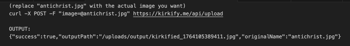
Howdy! you can probably just use the /api/upload endpoint that the actual site uses under the hood. just pass a file and it returns an outputPath object that tells you where to download the kirkified image. Though I'm gonna ask that you don't spam it.
1
2
355

20 Nov 2025
Programmieren (Skripten) mit KI Teil 2
Ich hatte ja neulich ein total verunglücktes Beispiel präsentiert. Hier nun ein weiteres, diesmal mit Googles Genimi, welches wesentlich besser lief.
Problem war - ich wollte rausfinden, auf welchen von und 100 Servern eine bestimmte VHDX gemountet ist. Ich kann da entweder jeden Server einzeln öffnen und nachschauen aber meine exorbitante Faulheit steht dem entgegen oder ich schicke einen AZUBI drüber aber der wird mich dafür nicht mögen. Außerdem muß ich da immer wieder mal nachschauen.
Also folgender mehrstufiger Prompt:
Schreib mir ein powershell script das alle windows server die mit "AVD-M" im Namenbeginnen abfragt und die verbundenenfestplattennamen pro server in eine csv datei schreibt.
Output kann ich leider nicht posten, denn es sind zu viele Cashtags drin, die X nicht akzeptiert.
Aber schonmal nicht schlecht, gar nicht schlecht aber ich sehe, get-ciminstance alleine wird nicht zum Ziel führen, also:
Verwende zusätzlich zum get-ciminstancebefehl auch diese befehle um es abzurufen.
Output schon fast perfekt aber ich konkretisiere:
Frage im script bitte alle server mit den Namen AVD-W11-M-0 -99 ab und verzichte auf eine AD-Abfrage.
# Definiert den Pfad für die Ausgabe-CSV-Datei
$outputPath =
"C:\temp\ServerFestplatten.csv"
# Erstellt eine Liste von Servernamen von AVD-W11-M-0 bis AVD-W11-M-99
$serverList = 0..37 | ForEach-Object { "AVD-W11-M-$_
" }
# Erstellt ein leeres Array, um die Ergebnisse zu speichern
$report = @()
# Durchläuft jeden Server in der definierten Liste
foreach ($serverName in $serverList) {
$cimSession = $null
Write-Verbose "Frage Festplatten für Server ab: $serverName"
# Prüft, ob der Server erreichbar ist
if (-not (Test-Connection -ComputerName $serverName -Count 1 -Quiet)) {
Write-Warning "Server $serverName ist nicht erreichbar.
"
$report = [PSCustomObject]@{
'Server'
= $serverName
'Festplattenmodell'
=
'Nicht erreichbar'
'Anzahl Partitionen'
=
'N/A'
'Volumebezeichnungen'
=
'N/A'
}
continue
}
try {
# Erstellt eine CIM-Sitzung für effiziente Remote-Befehle
$cimSession = New-CimSession -ComputerName $serverName -ErrorAction Stop
# Ruft alle Festplatten auf dem Remote-Server ab
$disks = Get-Disk -CimSession $cimSession
if ($null -eq $disks) {
$report = [PSCustomObject]@{
'Server'
= $serverName
'Festplattenmodell'
=
'Keine Festplatten gefunden'
'Anzahl Partitionen'
= 0
}
'Volumebezeichnungen'
''
=
continue
}
# Durchläuft jede Festplatte
foreach ($disk in $disks) {
# Ruft die zugehörigen Partitionen und Volumes ab, um die Bezeichnungen zu ex
$volumeLabels = $disk | Get-Partition -CimSession $cimSession | Get-Volume -C
$volumeLabelsString = $volumeLabels -join '
'
,
$object = [PSCustomObject]@{
'Server'
'Festplattenmodell'
'Anzahl Partitionen'
'Volumebezeichnungen'
= $serverName
= $disk.Model
= $disk.NumberOfPartitions
= $volumeLabelsString
}
$report = $object
}
}
catch {
Write-Warning "Fehler beim Abrufen der Festplatteninformationen von $serverName.
$report = [PSCustomObject]@{
'Server'
= $serverName
'Festplattenmodell'
=
"Fehler bei der Abfrage"
'Anzahl Partitionen'
=
'N/A'
'Volumebezeichnungen'
=
'N/A'
}
}
finally {
# Bereinigt die CIM-Sitzung
if ($cimSession) {
Remove-CimSession -CimSession $cimSession
}
}
}
# Exportiert den Bericht in eine CSV-Datei
if ($report.Count -gt 0) {
$report | Export-Csv -Path $outputPath -NoTypeInformation -Encoding UTF8
Write-Host "Bericht wurde erfolgreich nach $outputPath exportiert.
"
}
else {
Write-Host "Keine Server zur Verarbeitung gefunden.
"
}
Wow 😳 perfekt - ein überzeugendes Ergebnis. Das Script läuft einwandfrei uns es kommt eine wunderschöne CSV mit genau den Infos, die ich wollte. Hätte ich das, daß Array komplett selbst programmieren müssen, wäre ich lange, viele Stunden dran gesessen. So war das ein Job von nichtmal 10 Minuten.
Aber:
Ohne Kenntnisse in PowerShell-Scripting geht es nicht. Man muß die KI kontrollieren und den Output bewerten und korrigieren können. Wenn das jedoch gegeben ist, ist der Produktiovitätsgewinn enorm.
6
2
52
2,005

18 Aug 2025
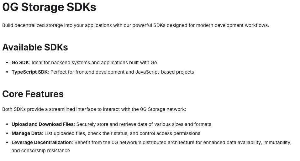
0G Storage SDKs 存储软件开发工具部署教程
你是不是也遇到过这种情况:文件放在传统云上,担心被删除、篡改、或者哪天就被审查了?去中心化存储看上去是个好方向,但很多项目一上来就让人劝退 —— 文档复杂、接口老旧、部署流程折磨人。
这次,0G 给开发者带来了一套「更像现代工具」的解决方案:0G Storage SDKs。
用起来的感觉就像是给应用加个 npm 包或者 Go 库一样自然,不用再自己啃底层的区块链交互。
---
两把钥匙:Go SDK 和 TypeScript SDK
〓Go SDK:非常适合后端服务,尤其是你已经在用 Go 写 API 或微服务的时候。
〓TypeScript SDK:天然适配 Web 应用、JS 工具链,前端开发者可以无缝接入。
无论选哪一个,核心能力都是一致的:上传、下载、数据管理,全都直接走 0G 网络。
---
能做什么?
这里简单列一下最常见的场景:
〓 文件上传 & 下载
把任何格式的文件存进去,再完整拿出来,底层自动帮你搞定分布式存储。
〓 数据管理
你可以列出上传过的文件,查状态,甚至细化访问权限。
天然的去中心化属性
文件不是放在某个单点服务器,而是分布式的,带来高可用、防篡改、抗审查。
换句话说:你得到的是 Web2 的体验 Web3 的安全性。
---
上手比你想象的快
0G 提供了 Starter Kit,基本就是「开箱即用」的模版项目:
〓 TypeScript Starter Kit:内置 Express.js 服务端 CLI 工具
〓 Go Starter Kit:自带 Gin 服务端 CLI 工具
直接跑起来就能体验完整流程,避免从 0 开始造轮子。
--
实操
假设你决定在后端用 Go SDK,那就这样开始:
1.安装
Install the 0G Storage Client library:
安装0G存储客户端库:
go get github.com/0glabs/0g-storage…
2.Setup 设置
Import Required Packages
导入所需的包
import (
"context"
"github.com/0glabs/0g-storage…"
"github.com/0glabs/0g-storage…"
"github.com/0glabs/0g-storage…"
"github.com/0glabs/0g-storage…"
)
Initialize Clients 初始化客户端
// Create Web3 client for blockchain interactions
w3client := blockchain.MustNewWeb3(evmRpc, privateKey)
defer w3client.Close()
// Create indexer client for node management
indexerClient, err := indexer.NewClient(indRpc)
if err != nil {
// Handle error
}
Parameters: 参数:
evmRpc: 0G Chain RPC endpoint (e.g., evmrpc-testnet.0g.ai/)evmRpc:0G链RPC端点(例如,evmrpc-testnet.0g.ai/)
privateKey: Your Ethereum private key for signing transactionsprivateKey:用于签署交易的以太坊私钥
indRpc: Indexer RPC endpoint (e.g., indexer-storage-testnet-turb…)indRpc:索引器RPC端点(例如,indexer-storage-testnet-turb…)
3.Core Operations 核心操作
Node Selection 节点选择
Select storage nodes before performing file operations:
在执行文件操作前选择存储节点:
nodes, err := indexerClient.SelectNodes(ctx, segmentNumber, expectedReplicas, excludedNodes)
if err != nil {
// Handle error
}
Parameters: 参数:
ctx: Context for operation management
ctx:操作管理上下文
segmentNumber: Identifies which storage segment to use
segmentNumber:标识要使用哪个存储段
expectedReplicas: Number of file copies to maintain (minimum 1)
expectedReplicas:要维护的文件副本数量(最少1个)
excludedNodes: List of nodes to exclude from selection
excludedNodes:要从选择中排除的节点列表
File Upload 文件上传
Upload files to the network: 将文件上传到网络:
// Create uploader
uploader, err := transfer.NewUploader(ctx, w3client, nodes)
if err != nil {
// Handle error
}
// Upload file
txHash, err := uploader.UploadFile(ctx, filePath)
if err != nil {
// Handle error
}
Parameters: 参数:
ctx: Context for upload operation
ctx:上传操作的上下文
w3client: Web3 client instance
w3client:Web3客户端实例
nodes: Selected storage nodes
nodes:选定的存储节点
filePath: Path to the file being uploadedfilePath:正在上传的文件的路径
File Hash Calculation 文件哈希计算
Calculate a file's Merkle root hash for identification:
计算文件的默克尔根哈希值以作识别:
rootHash, err := core.MerkleRoot(filePath)
if err != nil {
// Handle error
}
fmt.Printf("File hash: %s\n", rootHash.String())
File Download 文件下载
Download files from the network: 从网络下载文件:
// Create downloader
downloader, err := transfer.NewDownloader(nodes)
if err != nil {
// Handle error
}
// Download with optional verification
err = downloader.Download(ctx, rootHash, outputPath, withProof)
if err != nil {
// Handle error
}
Parameters: 参数:
ctx: Context for download operation
ctx:下载操作的上下文
rootHash: File's unique identifier (Merkle root hash)
rootHash:文件的唯一标识符(默克尔根哈希)
outputPath: Where to save the downloaded file
**outputPath**:下载文件的保存位置
withProof: Enable/disable Merkle proof verification (true/false)
withProof:启用/禁用默克尔证明验证(真/假)
Best Practices 最佳实践
Error Handling: Implement proper error handling and cleanup
**错误处理**:实施适当的错误处理和清理操作
Context Management: Use contexts for operation timeouts and cancellation
上下文管理:使用上下文来设置操作超时和取消机制
Resource Cleanup: Always close clients when done using defer client.Close()
**资源清理**:使用完毕后,始终使用 `defer client.Close()` 关闭客户端。
Verification: Enable proof verification for sensitive files验证:对敏感文件启用证明验证
Monitoring: Track transaction status for important uploads
监控:跟踪重要上传的交易状态
---
为了避免踩坑,可以注意以下几点:
〓 错误处理要全面:上传、下载、初始化都要有异常捕获。
〓 用 context 控制超时:不要让请求无限挂起。
〓 资源要清理:别忘了 defer client.Close()。
〓 验证下载:对敏感文件开启默克尔证明验证。
〓 状态监控:追踪交易状态,确保文件真的上链。
---
总结
如果说 IPFS、Arweave 给我们开了「去中心化存储」的大门,那 0G Storage SDKs 更像是把门口的台阶修平了, 让开发者真正能轻松落地。
前端可以直接用 TypeScript SDK
后端可以无缝接入 Go SDK
Starter Kit 帮你节省大量时间
如果你正在开发 DApp、去中心化 AI 应用,或者单纯想摆脱 Web2 的存储束缚,0G SDK 值得一试。
原文出处:docs.0g.ai/developer-hub/bui…
<0G忠实建设者:akiii >
@0G_labs @KaitoAI #0g_labs #KAITO
16 Aug 2025

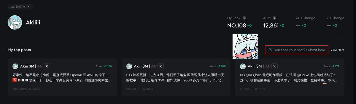
「0G 银河任务」系列圆满结束🎉
0G @0G_labs 不光和 kaito 合作
也有和 galxe 合作有排行榜
我发现很多文章不被识别
不要担心,点击这里即可手动提交
目前我在 Galxe 排行榜的排名为 108
91
76
20,716

12 Jul 2025
Step Functions: JSONataサポートで、従来のJSONPathベースのワークフローで使われていたフィールド(InputPath、Parameters、ResultSelector、ResultPath、OutputPath等)がArguments と Output の2つに簡素化された、とな📝
#cdkconf2025
2
267

2 Jun 2025
deploy caiu do nada depois da atualizacao do angular
tava buildando mas ia pro ar
fui pesquisando, doc antiga, mal dizia algo sobre
muraram o outputPath do build. por razao nenhuma. nao vai mais pra pasta especificada. agora é projeto/browser. nginx nao tava achando o index

1
2
47

4 Apr 2025
A few months ago, I stared at an AWS Step Function diagram and thought,
"Looks cool… but what the hell is going on here?"
Fast forward to now — I’m using Step Functions to orchestrate complex workflows with branching logic, parallel execution, and error handling for a project.
I wrote a guide that breaks it down:
✅ What exactly are states in a Step Function
✅ How data flows between steps using `InputPath`, `ResultPath`, `OutputPath`
✅ A simple example with 3 .NET Lambdas
If Step Functions ever felt overwhelming, this is the post I wish I had had when starting out.
Read: codewithmukesh.com/blog/aws-…
#AWS #StepFunctions #Serverless #CloudDevelopment #DevJourney #DotNet #Developers

1
6
449

Check the param line. It sets output path to c:\github\private… then at the bottom typo “geneterate” $outputpath = $outpath\filename.html. Maybe set a default path of wherever the script is ran. The \ will fail on osx paths.
2
2
406

27 Feb 2024
I like:
- very powerful way to create state machines
- possibility for zero-code workflows
I miss:
- "merge" output with input (not just OutputPath)
- More intrinsic functions (now(), uuid(), etc)
2
4
261

27 Oct 2023
最低限、ResultPathだけ他のタスクから書き換えたり干渉しないように明確に決めておいて、各タスクで使う時に必要なpathから読み込む、とういうのが現実的なのかなと思っています
InputPathとかOutputPathとかResultSelectorは、毎回「なんだっけ…?」と忘れるし、使わなくてもそんなに困らない
27 Oct 2023

Step Functions使うときにInput/Outputなどの方針決めないとぐっちゃぐちゃになってヤバいな
2
8
2,814

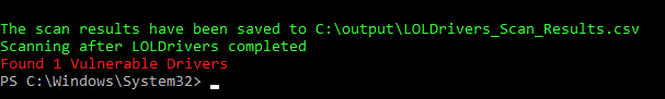
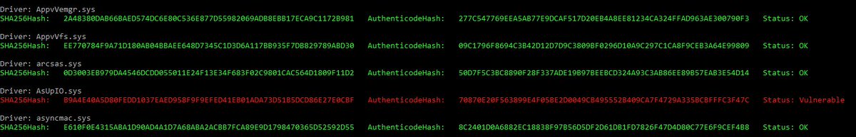
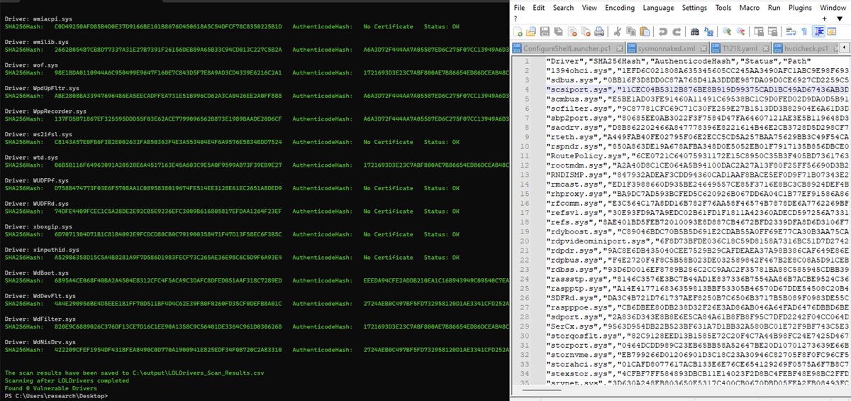
🚀 Updated the ever-popular Scan-Drivers/Scan-LOLDrivers utility for scanning #LOLDrivers!
It seems that both @IISResetMe (gist.github.com/IISResetMe/1…) and I stumbled upon the same issue. 🤔 But, I've given it a boost! 🚀
I remove the use of Get-AppLockerFileInformation and switched to System.Security.Cryptography.X509Certificates.X509Certificate2 for authenticode.
The result? It's now compatible across platforms and super speedy! ⚡
Check it out here: github.com/MHaggis/notes/blo…
For those using PwSh 7 on Server 2019, here's how to run it:
Invoke-Expression (Invoke-RestMethod -Uri "raw.githubusercontent.com/MH…"); Scan-Drivers -DriverPath "C:\windows\system32\drivers" -FileFilter "*.sys" -Output "CSV" -OutputPath "C:\output"
And for the Win11 PwSh 7 users, it's the same one-liner! 🎉 (Note: No vulnerable drivers found, which is the expected output)
1
5
22
4,818

7 May 2023
Some days I really love #PowerShell #GitHub Actions:
[PSObject].Assembly.GetTypes() |
? IsPublic |
TypesByNamespace📊 -OutputPath (
Join-Path $docsRoot "PowerShell-Types-By-Namespace.html"
)
Becomes
psmetrics.start-automating.c…
Thanks to
github.com/StartAutomating/P…
4
10
1,999

14 Apr 2023
勝ちました。
シーン内で選択したカメラだけを、ファイル名+カメラ名で、再読み込みとかせずにジャンジャン書き出してくれるスクリプトです。
今はパス固定だけどw
(function() {
var currentFilename = Scene.getFilename();
var splitPath = currentFilename.split("/");
var filename = splitPath[splitPath.length - 1].toLocaleLowerCase().replace(".duf", "");
var viewportMgr = MainWindow.getViewportMgr();
var cameras = Scene.getSelectedCameraList();
for (var camNum = 0; camNum < cameras.length; camNum ) {
var viewport = viewportMgr.getActiveViewport().get3DViewport();
viewport.setCamera(cameras[camNum]);
var camera = viewport.getCamera();
var filenameWithCameraLabel = filename camera.getLabel();
var outputPath = "D:\\daz\\Render\\daz\\dazkuso\\" filenameWithCameraLabel.toLocaleLowerCase() ".png";
var renderMgr = App.getRenderMgr();
var renderer = renderMgr.getActiveRenderer();
var renderOptions = renderMgr.getRenderOptions();
var currentViewport = viewportMgr.getActiveViewport();
var current3DViewport = currentViewport.get3DViewport();
var frameRect = current3DViewport.getAspectFrameRect();
var frameWidth = frameRect.width;
var frameHeight = frameRect.height;
var frameAspect = frameWidth / frameHeight;
renderOptions.renderImgToId = DzRenderOptions.DirectToFile;
renderOptions.renderImgFilename = outputPath;
renderOptions.imageSize = new Size(frameWidth, frameHeight);
renderOptions.isCurrentFrameRender = true;
var timeRange = new DzTimeRange(renderOptions.startTime, renderOptions.endTime);
var renderHandler = new Dz3DViewRenderHandler(currentViewport, timeRange.start, outputPath);
renderer.render(renderHandler, camera, renderOptions);
}
})();
1
3
221

22 Mar 2022
Is it possible for #aws Step Functions to understand `undefined`?
E.g.
Type: Pass
OutputPath: $.a
InputPath: $.variable.prop
If InputPath `$.variable.prop` doesn't exist, would it make sense to delete OutputPath $.a instead of throwing an error?
TS equiv.
a = variable?.prop;
1
3

6 Nov 2021
of course you have to extract the frames first and delete the ones where the object isn't visible
ffmpeg -i videoclip.mp4 /outputpath/d.png
2

8 Oct 2021
配置したパス/realesrgan.exe -i inputpath -o outputpath -n realesrgan-x4plus-anime
でうまくいくと思います
2
1