
Joined September 2012
- Tweets 504
- Following 130
- Followers 265
- Likes 379
87 Photos and videos


10 Mar 2023
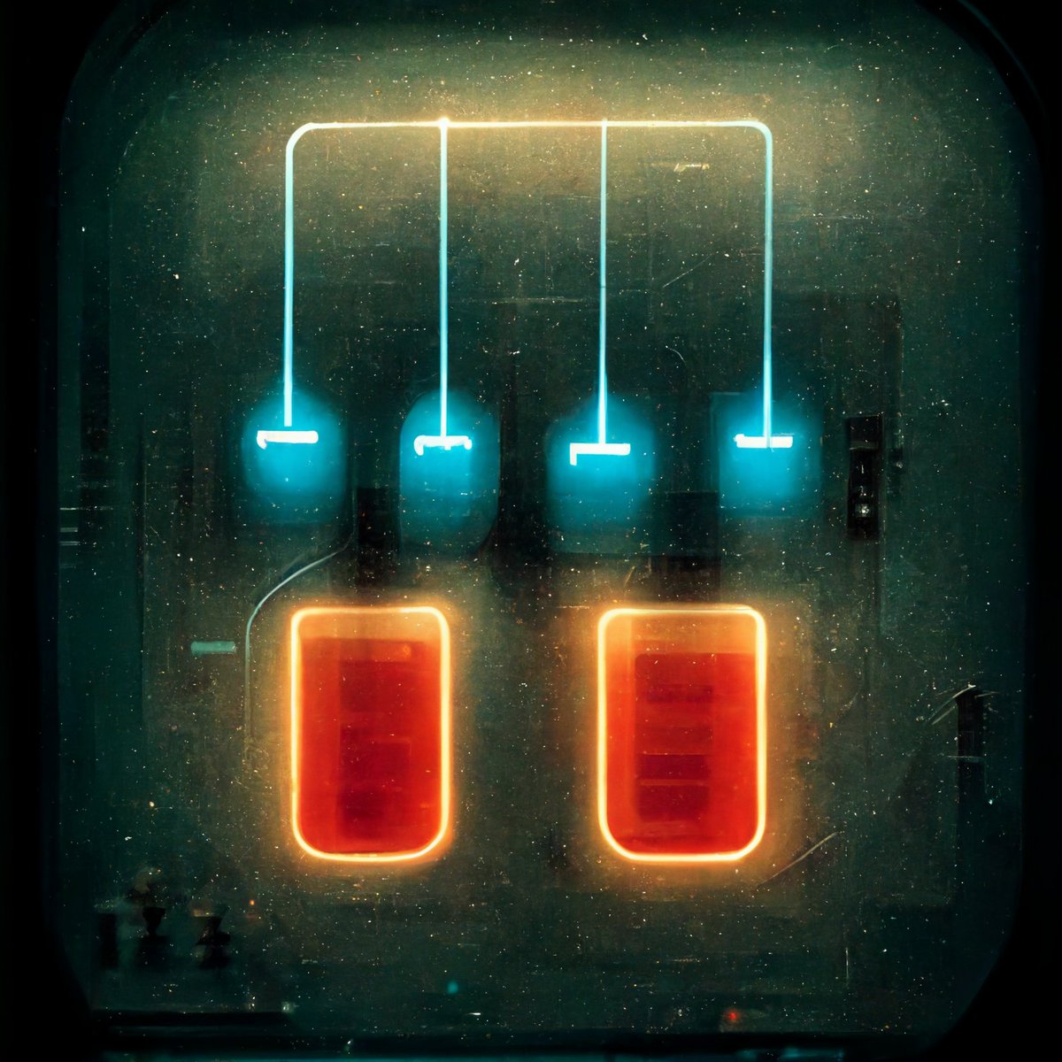
Some of the analog cells might look good as 3d prints :) Pre-heat my plate!

printed the cells included in the new #IHP PDK here:
colab.research.google.com/gi…

1
2
382
25 Oct 2022
#YetToComeBusan knocked me of my feet and left me in a dancing loop on repeat. I wanna go concerts again!
18 Oct 2022
37c3 Canceled. And what exactly am i supposed to do between Christmas and new year instead? events.ccc.de/#no-congress-2…
3
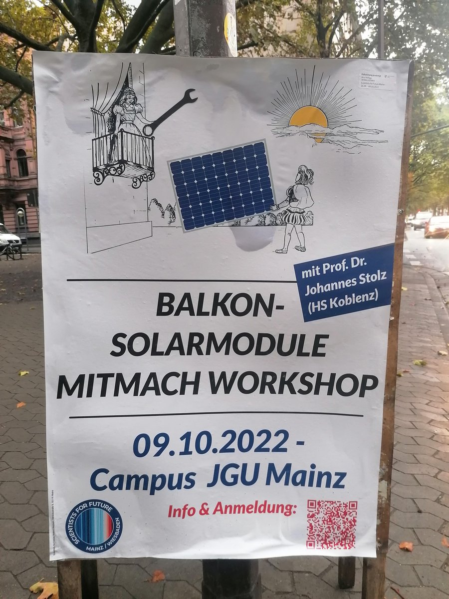
1 Oct 2022
Cool! DIY Workshop for solar modules on the own balcony at home. Uni Mainz.
1
28 Sep 2022
Great interview about the "how to" of creating open-source PDKs and standard cells.
24 Sep 2022

Talking standard cell libraries with @JamesStineJr !
How many cells do you need?
What do engineers least understand?
Why do we need one for @GlobalFoundries 180nm?
Are there any circuit families from the past that deserve new attention?
youtube.com/watch?v=5J8LJoUx…
1
4
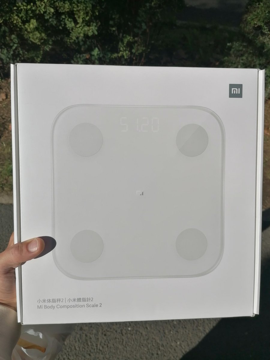
21 Sep 2022
Welcome to the family: My new mobile is the Xiaomi Scale 2 Squarephone /w 4-digit 7-segment speed dial - just step on it.
21 Sep 2022
Goodbye weekend plans. No sunshine, no long autumn walks, just plain being inside in front of the computer.
store.steampowered.com/app/2…
1
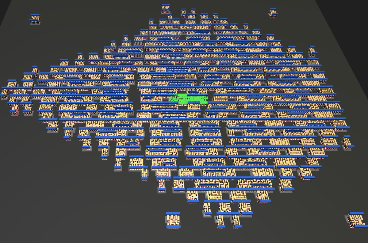
14 Sep 2022
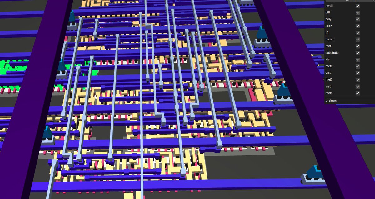
Mission: Explore my own #tinytapeout (tto) design with the 3D viewer by @maxiborga and @proppy. Accomplished: My 8-bit-pattern-player with their interactive viewer: thorkn.github.io/wokwi-veril… Try out cell highlighting and the 1,2,3 keys. This is perfect for student lectures!
3
6
13 Sep 2022
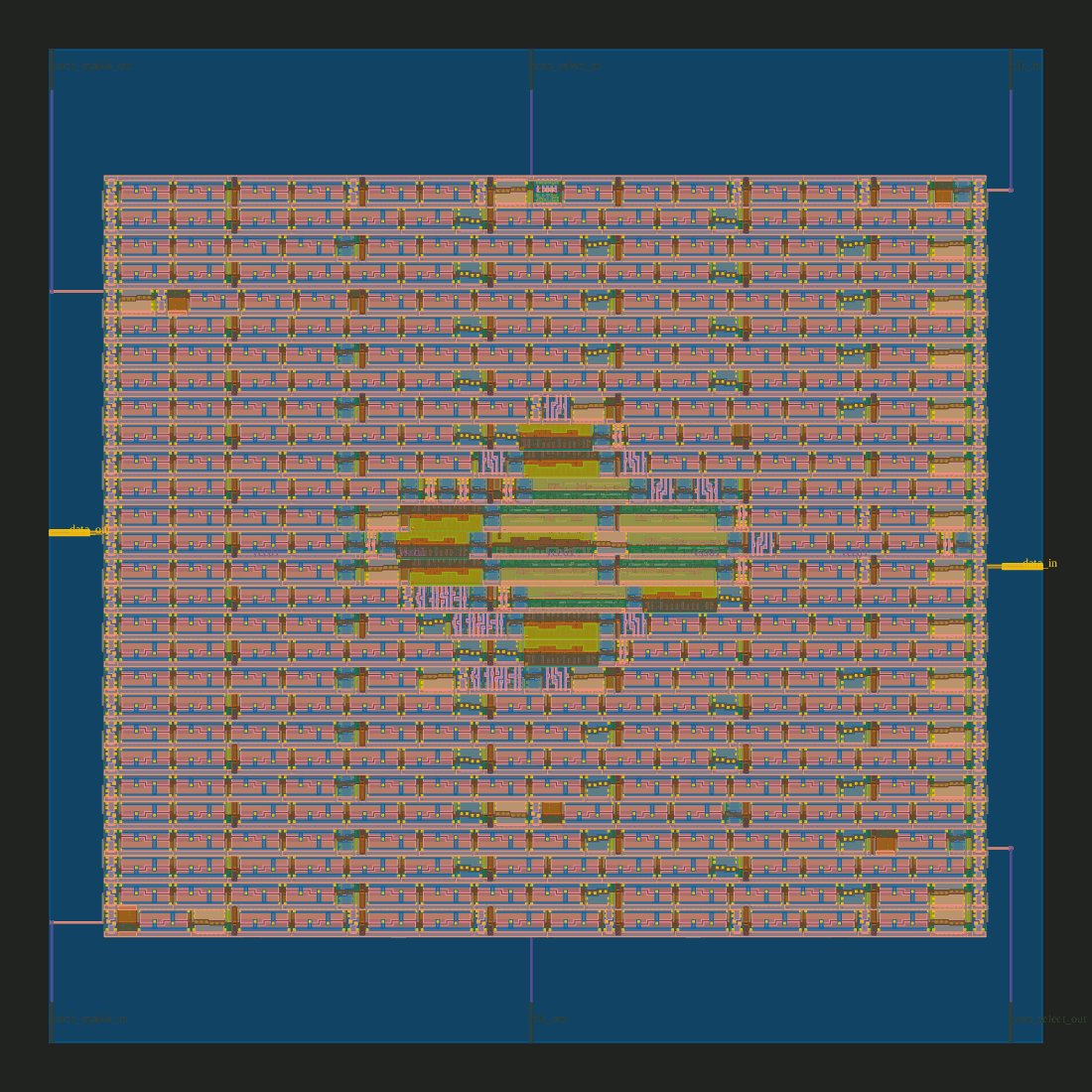
This is so damn beautiful that it makes me sick. Exploring #tinytapeout designs in an intuitive graphical way. Congrats @proppy and @maxiborga.
13 Sep 2022
Check out this excellent upgrade to #tinytapeout build system by @proppy & @maxiborga - An interactive 3D viewer of the GDS!
Even does cell highlighting and layer control.
mattvenn.github.io/wokwi-ver…
2
13 Sep 2022
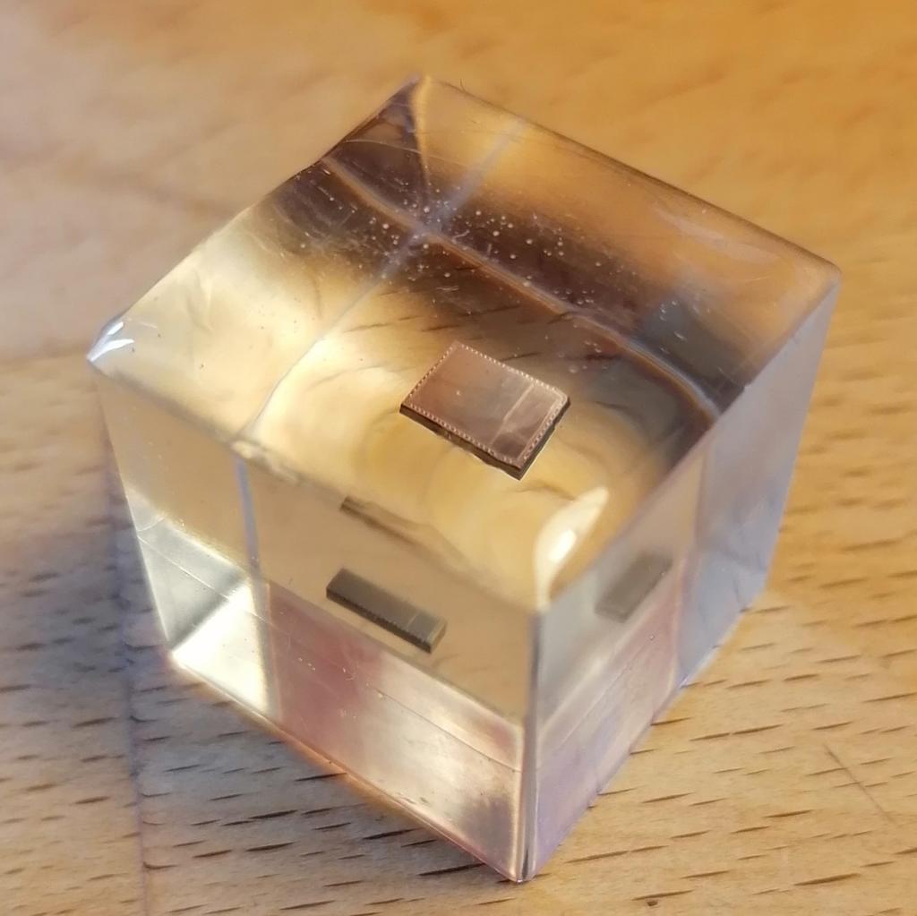
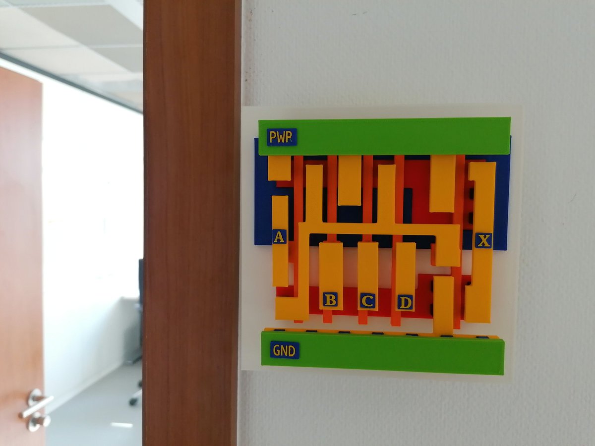
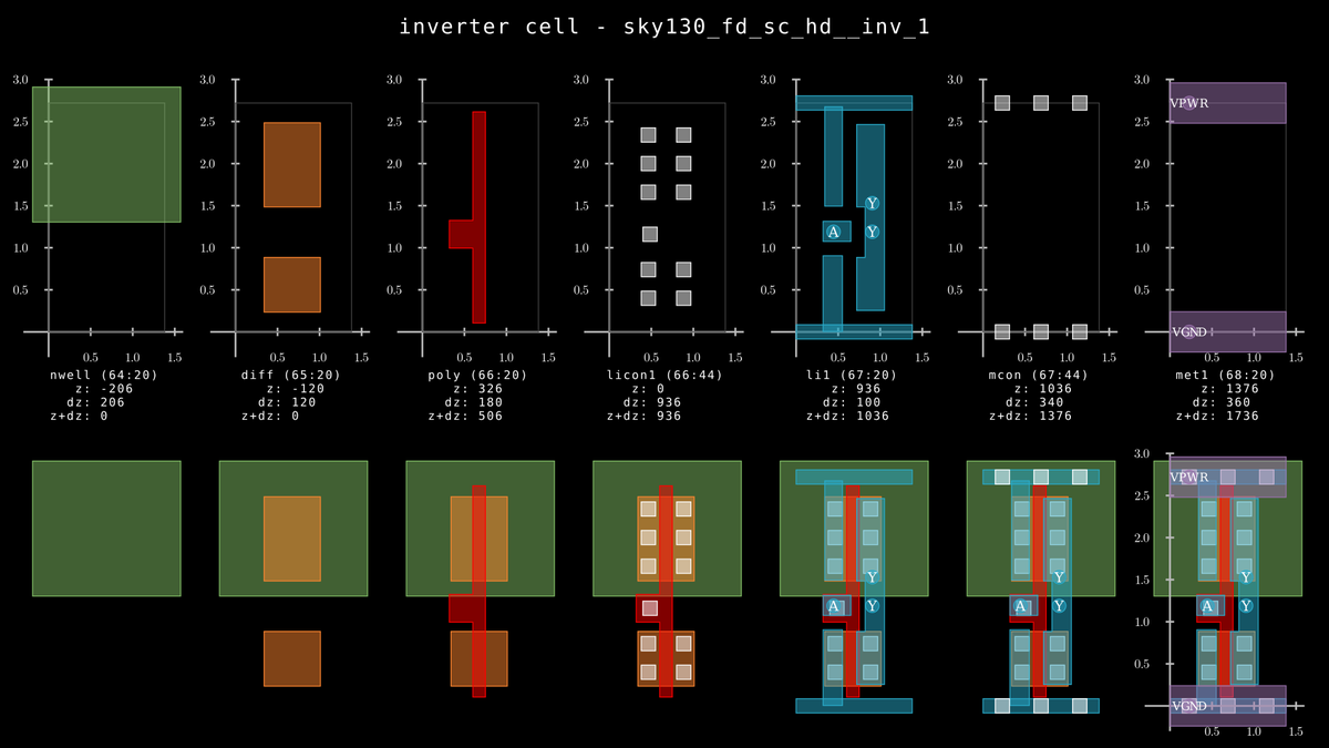
A great picture to understand the stacking of #SKY130 layers in the standard cells. And good for glueing together 3d cell models ;)
7 Oct 2021

Layers of an Inverter Cell in the #SKY130 nanometer CMOS process node from @SkyWaterFoundry. The motivation behind this is to inspect the order in which the layers position on top of one another, and spot the correspondence to the digital circuit diagram.
2
3
6 Sep 2022
My how-to guide on 3D-printing standard cells from the Open-source SKY130 PDK. Thanks to @matthewvenn and his fantastic Zero-to-ASIC course and @maxiborga for the modified gdsiistl. #sky130 link.medium.com/aREGNL4T6sb
5
24
114
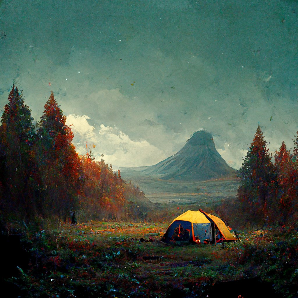
3 Sep 2022
AI generated artwork. This is my very first try with #midjourney, topic #camping. Damn, there goes my saturday... hooked onto playing with an AI. Weird, challenging and frightening at the same time. @midjourney
1
4
1 Sep 2022
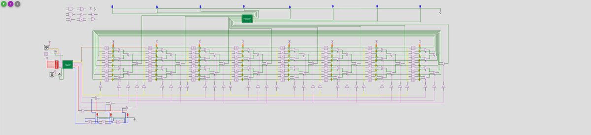
#tinytapeout is addictive! This is my third submitted design, there are some hours left till deadline and i still think about doing another one. @matthewvenn github.com/ThorKn/tinytapeou… wokwi.com/projects/341620484…
3
16
31 Aug 2022
I submitted an capture-the-flag chipdesign to #tinytapeout. A 40 Bit number is hardcoded into the chip and must be found to enable the output pin to high. I don't know if this idea will work, but it is a ton of fun to build chips for tinytapeout.com @matthewvenn
2
2
19
31 Aug 2022
The design is done with wokwi wokwi.com/projects/341516949… and is prepared for tinytapeout in this Git repo: github.com/ThorKn/tinytapeou…
31 Aug 2022
My very own 8-bit shiftregister shall be produced as a microchip :) See for yourself on how to do this at tinytapeout.com . The design and the submission took me only 30 Minutes. Digital chipdesign has never been easier. Go go go! @matthewvenn #tinytapeout
1
4
12
31 Aug 2022
And here are the project urls: wokwi.com/projects/341506274… github.com/ThorKn/tinytapeou…
13 Jul 2022
Thank you @matthewvenn for this awesome piece of MPW-1. I will treasure and use it. Real meetings and conferences enable the exchange of such goodies again. Awesome FSiC in Paris! #FSiC2022 #sky130 #zerotoasic
1
6