
TG channel: t.me/fionasdailynews
Joined May 2018
- Tweets 12,950
- Following 719
- Followers 47,211
- Likes 10,170
2,030 Photos and videos


Pinned Tweet

May 23
为何会提出光互连解决当前HBM封装的极限?
最本质的原因是:我们正在一步步接近HBM封装的极限。
一、物理规律的极限被逐渐触及:
极限1️⃣:垂直堆叠层数——已触顶
HBM的堆叠演进:HBM2(8层)→ HBM2E(8层)→ HBM3(12层)→ HBM3E(12/16层)→ HBM4(计划16–20层)。
每多叠一层,TSV(硅穿孔)的深宽比就要提高。目前16层的TSV深宽比约为20:1,这是电镀铜填充工艺的极限边缘——再往上,铜填充时气泡无法逸出,良率断崖式下跌。
更深的问题是热阻叠加。每层DRAM die的导热路径要穿越所有下层芯片才能到达散热器。12层堆叠时底层die的结温(junction temperature)比顶层高约15°C,20层时这个差距会超过25°C,已经超过DRAM工作安全边界。
这都导向一个事实——垂直方向的物理扩展空间已所剩无几。
极限②:硅中介层岸线——已触顶
GPU的「岸线」(shoreline)是GPU die四周边缘的物理周长。HBM堆栈通过硅中介层与GPU并排,HBM的数量上限就是:GPU周长能容纳多少个HBM接口宽度。
假设GPU die最终做到一个reticle极限,周长约为130mm,单个HBM4堆栈接口约需4mm,理论上限约为32个堆栈——但实际上电源/信号走线、角落利用率等因素会把这个数字压到16–20个以内。
极限③:带宽密度(单位面积IO数)——接近极限
Microbump的物理极限大约在25–30μm pitch,低于这个数字,焊锡球的表面张力和对准精度无法维持量产良率。
极限④:功耗密度——这是最被低估的极限
HBM3E每栈满载功耗约15W,8栈就是120W,加上GPU本身的600–700W,整个封装的功耗密度已经超过100 W/cm²,相当于火箭发动机喷口附近的热流密度。
散热才是最硬的物理墙。
HBM越叠越高,散热路径越长,这是垂直堆叠无法回避的热阻叠加问题,与材料科学的边界直接碰撞。
—————————————————————————
二、光连接的解法
电信号传输本质上是在用「极短距离」这个物理条件换取优势。
光的优势恰好在电的弱点处显现——光信号的带宽与距离几乎无关。当GPU与HBM的物理间距被迫增加,光互连的相对优势就从「理论上可行」变成「工程上合理」。
—————————————————————————
三、目前技术架构的可能形态
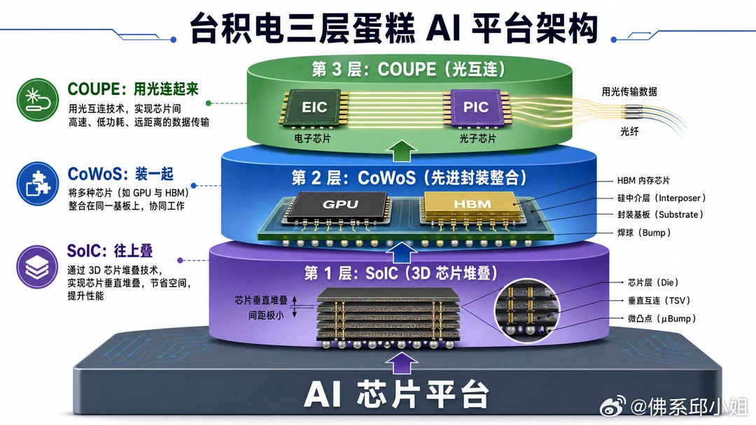
方案A:光学Bridge芯片
在硅中介层中嵌入硅光子波导层,GPU与HBM之间的信号不再走铜线,而是走片内波导。距离仍在毫米级,但打破了「必须紧邻」的约束,允许HBM在中介层上远离GPU边缘排列。
这是Ayar Labs(与Intel合作)的TeraPHY路线,已在2024年实现单chiplet 2Tbps光I/O,且可3D堆叠于逻辑芯片下方。
方案B:CXL over Optics(推理情况不合适)
将多个HBM堆栈聚合为独立的记忆体池模块,通过CXL协议与GPU通信。距离可达几厘米至数十厘米,直接接入背板。这不是HBM专属光互连,而是把HBM变成CXL记忆体节点。
延迟代价:每次E→O→O→E转换约增加5–10ns,相对于DRAM本身的~150ns访问延迟,约增加3–7%,在大模型训练的流式访问模式下可接受,但推理场景(延迟敏感)会更在意。
方案C:3D光学垂直互连(最激进)
将HBM置于GPU正下方,利用垂直光学通孔(Optical Through-Silicon Vias,OTSV) 实现Z轴方向的光互连。这在理论上消灭了岸线限制(HBM直接在GPU下方大面积铺展),同时保持极短传输距离。
方案D:光子织网
把光子互连fabric做成一个独立的2D芯片层,像三明治一样插在GPU和HBM(或其他加速器)之间,所有芯片通过这层光子层通信。它并不限定是HBM,而是一个通用的光互连基板。
—————————————————————————
四、这个方案的难点:激光源
这是目前工程界最头疼的问题。
硅不能发光。硅光子可以导光、调制光、探测光,但无法产生光。今天所有硅光子方案的激光源都是III-V族化合物半导体(InP、GaAs基材料),需要外置激光器,通过fiber coupling耦合进硅波导。
这带来:
可靠性问题:激光器是光互连系统中寿命最短的组件
良率问题:光纤与波导的耦合对准精度要求亚微米级,大规模封装良率极低
成本问题:III-V激光器目前仍比硅便宜不了多少,难以摊薄
功耗问题:激光源本身的电光转换效率约30–40%,是额外的能耗来源
————————————————————————
五、解决路径:
1️⃣直接在硅上外延生长III-V材料
Intel、MIT林肯实验室、UCSB都在研究,但良率与可靠性尚未达到量产标准。
2️⃣另一条路是量子点激光器直接长在硅上,理论上可行但仍是实验室阶段。
AXT(AXTI)的潜在价值就在这里——其磷化铟(InP)基片是高性能光互连激光器的关键衬底材料,这条需求链条目前仍处于早期。
————————————————————————
六、时间线
2026–2027:板级CPO(GPU与光引擎共封装)进入量产,主要用于scale-out网络,不直接涉及HBM
2027–2029:光学Bridge方案开始进入高端AI加速器概念验证,HBM可能扩展至更远位置但仍在同一封装内
2029–2032:CXL over Optics的记忆体池化开始规模部署,HBM功能性分离
2032 :真正意义上GPU-HBM光互连作为标准封装方案,仍存在不确定性


Breaking the "Memory Wall": Optical Interconnects Emerge in GPU–HBM Packaging
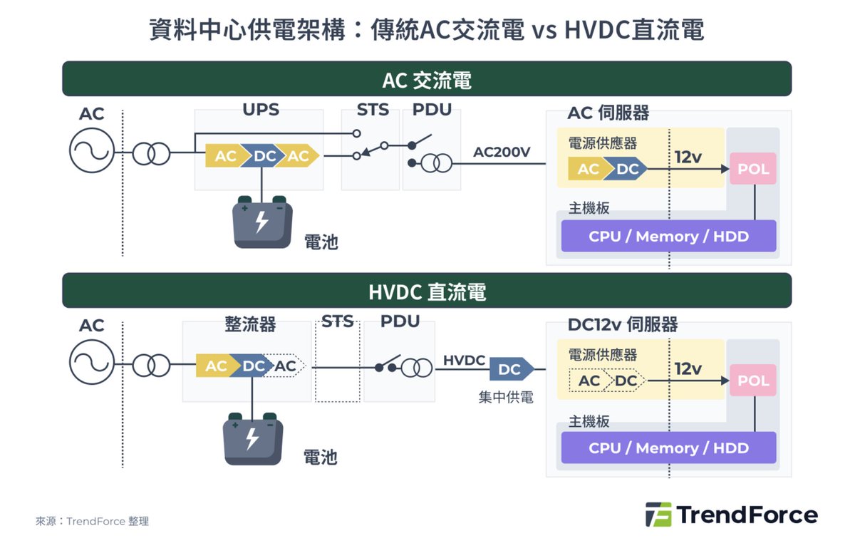
As a solution to the "memory wall," one of the chronic challenges in AI semiconductors, the memory and packaging industries at home and abroad are weighing an approach that decouples the GPU and high-bandwidth memory (HBM) and packages them separately. The core idea is to move the HBM—until now mounted right next to the GPU—a certain distance away, and bridge the gap with light (optics), allowing several times more HBM to be installed than is possible today.
On the 22nd, a researcher at a major domestic memory maker said, "We're currently struggling to expand HBM bandwidth and capacity, so we're discussing with customers a plan to overcome the GPU's shoreline limit through optical interconnects and mount more HBM." Shoreline refers to the length of the chip's perimeter.
In today's AI computing environment, the key factor dragging down compute efficiency is the data transfer speed of memory chips. While GPU performance has grown by leaps and bounds with each generation, the speed at which memory stores and supplies data has failed to keep pace—creating a structural performance barrier, the memory wall. The arrival of HBM, with its wide data pathways, put out the immediate fire, but critics continue to point out that bandwidth and transfer speeds still fall short of handling the explosive growth in AI compute.
Until now, the industry has focused on stacking HBM ever higher to increase memory capacity and bandwidth within a confined footprint. But as stack counts climbed past 12 and 16 layers toward 20 and beyond, process difficulty rose exponentially. The technology hit physical limits, including the growing difficulty of meeting fixed height specifications. Vertical stacking has reached an inflection point—so much so that the JEDEC standards body has relaxed its HBM height specifications.
The bigger problem is that if stack counts can't be raised, the alternative is to add more HBM horizontally around the GPU—but that, too, is impossible. In the current 2.5D packaging structure, the GPU and HBM are mounted tightly together on a single substrate. Within this structure, the number of HBM units that can be placed is strictly limited by the finite length of the GPU chip's perimeter—its shoreline. Even when more HBM is desired, there is physically no room to place it, leaving the industry in a structural deadlock.
The alternative now emerging across the semiconductor industry is to separate the GPU and HBM and package them independently. It overturns the conventional chip-design principle that components must sit close together to minimize data transfer time. Instead of keeping the two chips adjacent, the approach spaces them apart and links them with overwhelmingly fast optical signals to overcome the added physical distance.
Placing the HBM slightly away from the GPU within the board frees the design from the GPU's shoreline constraint. With the spatial limitation gone, far more HBM can be spread out laterally and packed into the board—several times more than today—without having to push stack heights to extremes. This means the total memory capacity and data bandwidth of the AI accelerator system would expand dramatically, on a scale incomparable to current systems.
"Discussing Placing HBM Beneath the GPU"… Form Factor Could Change
The industry is now producing a range of architectural design proposals over where exactly to place the HBM within the GPU board.
The same memory researcher said, "Options under discussion range from broadly utilizing the space immediately around the GPU to isolating the HBM beneath the GPU board." He added, "In the latter case—isolating it beneath the GPU board—the motherboard would have to be extended lengthwise, so we're discussing even an overall form-factor change with the GPU maker." Specifically, the HBM might surround the GPU from several centimeters away, or a separate HBM zone might be created in the center of the board.
"We're keeping every possibility open as we discuss the optimal layout," he said. "Nothing has been confirmed as an official roadmap yet, but as part of preliminary research toward next-generation AI accelerators, we're in talks with our partners."
The outsourced semiconductor assembly and test (OSAT) industry is also watching this trend closely. An executive at a global OSAT firm said, "Optical interconnects are a clear trajectory. The only question is timing," predicting that "rack-to-rack and server-to-server links will go optical first, and then chip-to-chip connections within the board will follow." He added, "The larger units will be connected by light first, but optical research is moving so fast that it may not be that far off."
Technically, the optical-interconnect technology linking GPU and HBM shares the same underlying principle as the technology connecting server to server inside a data center. The difference is the high technical barrier of shrinking optical-conversion technology—once used for communication between large pieces of equipment—down to the microscopic scale of a single board and chipset.
An executive at a domestic developer of co-packaged optics (CPO) components explained, "As HBM stack heights approach their limit, the industry is discussing spreading the memory out laterally to maximize how much can physically be mounted." He added, "The principle is the same as conventional data-center optical interconnects, but HBM optical links that have to operate within a confined board space require optical components to be miniaturized to far smaller sizes and far higher integration density—so the technical difficulty is greater."
17
50
237
107,717
19h
炒过美股的人很难回去炒A股,毕竟没那么多人是高手或者受虐癖。
其实我在过去一年多遇到不少朋友撺掇我买A股的。当然我知道自己的水平,在A股市场很难存活。
更重要的是,我花了无数的时间和精力,才完全了资金的全面去中国化,我很享受在中国当一个无产阶级的感觉。怎么可能再把钱汇回来?
17
4
52
13,442
21h
这一事件对于AI产业链的影响也是巨大的。
“审查”这一次国人应该不陌生了,“先进模型”过审成为了下一步的趋势。
这对美国 AI 创新环境也会产生“寒蝉效应”,使企业在推出高端模型前不得不进行更保守的内测和合规审查。
如果关键模型能力随时会被撤回,加大自研或开源路线投入也是各大公司必选之路。
对云厂商和大模型基础设施公司而言,“政策风险”这一因子的重要性也要重新评估。
中国、欧洲、俄罗斯等国也要加快自己的模型迭代,还是自己最靠得住。
21h

最近AI逆风的消息有点多,不过市场总是这样,坏消息都是接踵而逝的。
今天最重要的新闻是“Anthropic的Fable 5和Mythos 5被美国商务部以出口管制指令强制下架,所有用户失去访问权限,包括美国本土用户。”
事情背景:三天上线即被封杀
最初的政治指令要求“暂停所有外国国民(foreign nationals)对这两款模型的访问”,无论身在美国境内还是境外,甚至包括 Anthropic 自己的外籍员工。
一刀切:
Anthropic 表示,难以在短时间内准确识别所用户国籍身份,因此只能选择一刀切,全线下线。
官方原因:国家安全
多家媒体(CNBC、Axios 等)引用美国官员的话称,“另一家公司声称成功破解了 Mythos 的安全防护机制”。商务部在致 Anthropic 的函件中,将此上升到出口管制与国家安全层面。
阴谋论 瞎猜:
1️⃣政府与Anthropic之前冲突历史:Anthropic此前坚持AI 军事用途两条红线,而国防部要求移除,矛盾升级导致国防部合同续约谈崩。
2️⃣特朗普个人对其的厌恶:今年2月27日特朗普下令联邦政府全面停用 Anthropic,理由是该公司“试图用极左价值观左右美国军队如何作战”。
3️⃣先进AI模型成为下一步的出口限制:美国把最前沿通用大模型逐步纳入类似“高端 GPU / EDA 软件”的出口控制框架,属于“AI 卡脖子”新阶段。
5
11
9,360
21h
最近AI逆风的消息有点多,不过市场总是这样,坏消息都是接踵而逝的。
今天最重要的新闻是“Anthropic的Fable 5和Mythos 5被美国商务部以出口管制指令强制下架,所有用户失去访问权限,包括美国本土用户。”
事情背景:三天上线即被封杀
最初的政治指令要求“暂停所有外国国民(foreign nationals)对这两款模型的访问”,无论身在美国境内还是境外,甚至包括 Anthropic 自己的外籍员工。
一刀切:
Anthropic 表示,难以在短时间内准确识别所用户国籍身份,因此只能选择一刀切,全线下线。
官方原因:国家安全
多家媒体(CNBC、Axios 等)引用美国官员的话称,“另一家公司声称成功破解了 Mythos 的安全防护机制”。商务部在致 Anthropic 的函件中,将此上升到出口管制与国家安全层面。
阴谋论 瞎猜:
1️⃣政府与Anthropic之前冲突历史:Anthropic此前坚持AI 军事用途两条红线,而国防部要求移除,矛盾升级导致国防部合同续约谈崩。
2️⃣特朗普个人对其的厌恶:今年2月27日特朗普下令联邦政府全面停用 Anthropic,理由是该公司“试图用极左价值观左右美国军队如何作战”。
3️⃣先进AI模型成为下一步的出口限制:美国把最前沿通用大模型逐步纳入类似“高端 GPU / EDA 软件”的出口控制框架,属于“AI 卡脖子”新阶段。
3
24
17,396
22h
恭喜我们度过了6月的第二周,在月初的风险事件排名里,我认为并不重要的非农给市场好好上了一课。
虽然在第n次达成协议的边缘市场给了一些反弹,但是目前资金还是非常犹豫。
下周的fomc和四巫日,以及美光 $MU 的财报,才是市场真正要迎接的大考时间。
我目前策略是不加杠杆,不追高。跌到心理价位就分批加仓。本周内日韩股的加仓比例高过了美股。
Jun 2
都说sell in May and walk away,6月2日了,我还是满仓,还是每天疯狂学习AI。依旧看好AI的未来和我的账户的未来。
但是也确实担心6月整体市场会有什么不利因素,因此在月初来梳理一下这个月的风险因子。
1️⃣6月5日,【美国5月失业率】➕非农
前值:4.30% 预期:4.30%
2️⃣6月10日,【5月CPI年率】
3️⃣6月12日,SpaceX 上市。
🌟4️⃣6月16-17日
换主席后的第一次FOMC利率决议,将同步更新2026-2027年利率路径预测
🌟5️⃣6月18日/19日,四巫日
有假日,所以实际上的四巫日应该是6.18,历史上成交量和波动率显著放大
🌟6️⃣6月24日 美光财报日
伊朗问题我觉得已经不是主要扰动因素了,对市场会有影响但不是核心因素。
1
5
33
10,922
22h
之前就建议大家,如果想要从加密转来做股票交易,好好开一个正经券商账户,不要图方便,偷小懒吃大亏。
看到这次很多人用币圈CEX打新,结果似乎没有份额,“一堆交易所拿了 SpaceX IPO 的额度打算卖给币圈人,大半个币圈人都掏钱参与打新了,现在打完了,告诉你没额度,退款还要给几百刀的手续费。”
好好做个参加券商的国际配售没那么难,门槛也没那么高。
都被骗这么多次还要执着于此的话,我是真的不知道说什么了
16
3
45
17,378
Jun 13
互联网所创造的信息平等,自由。如今AI却可能剥夺这一切。
被分级筛选过的AI能力匹配给不同人,重新创造信息的壁垒和阶级。
9
24
14,047
Fiona ❤️& ✌️ retweeted

Jun 12
币圈彻底爆炸了,整个币圈都被割了。
一堆交易所拿了 SpaceX IPO 的额度打算卖给币圈人,大半个币圈人都掏钱参与打新了,现在打完了,告诉你没额度,退款还要给几百刀的手续费。
最惨的是,有人看到 $SPCX 盘前合约涨了很多,先通过做空来套保,锁定利润,结果套保的空单浮亏了,IPO 的股票现货还拿不到。
币圈炒作了几年的 RWA 币股叙事,经此一战,以后谁还敢玩 😭
519
92
1,470
600,297
Jun 13
美国政府:暂停所有人访问 Fable 5 和 Mythos 5
以后权贵阶级能用的AI和普通人能用的AI差距只会越来越大
Jun 13

The US government, citing national security authorities, has issued an export control directive to suspend all access to Fable 5 and Mythos 5 by any foreign national, whether inside or outside the United States, including foreign national Anthropic employees.
The net effect of this order is that we must abruptly disable Fable 5 and Mythos 5 for all our customers to ensure compliance.
Access to all other Claude models is not affected.
We apologize for this disruption to our customers. We believe this is a misunderstanding and are working to restore access as soon as possible.
Read our full statement: anthropic.com/news/fable-myt…
18
1
36
11,428
Fiona ❤️& ✌️ retweeted

Jun 12
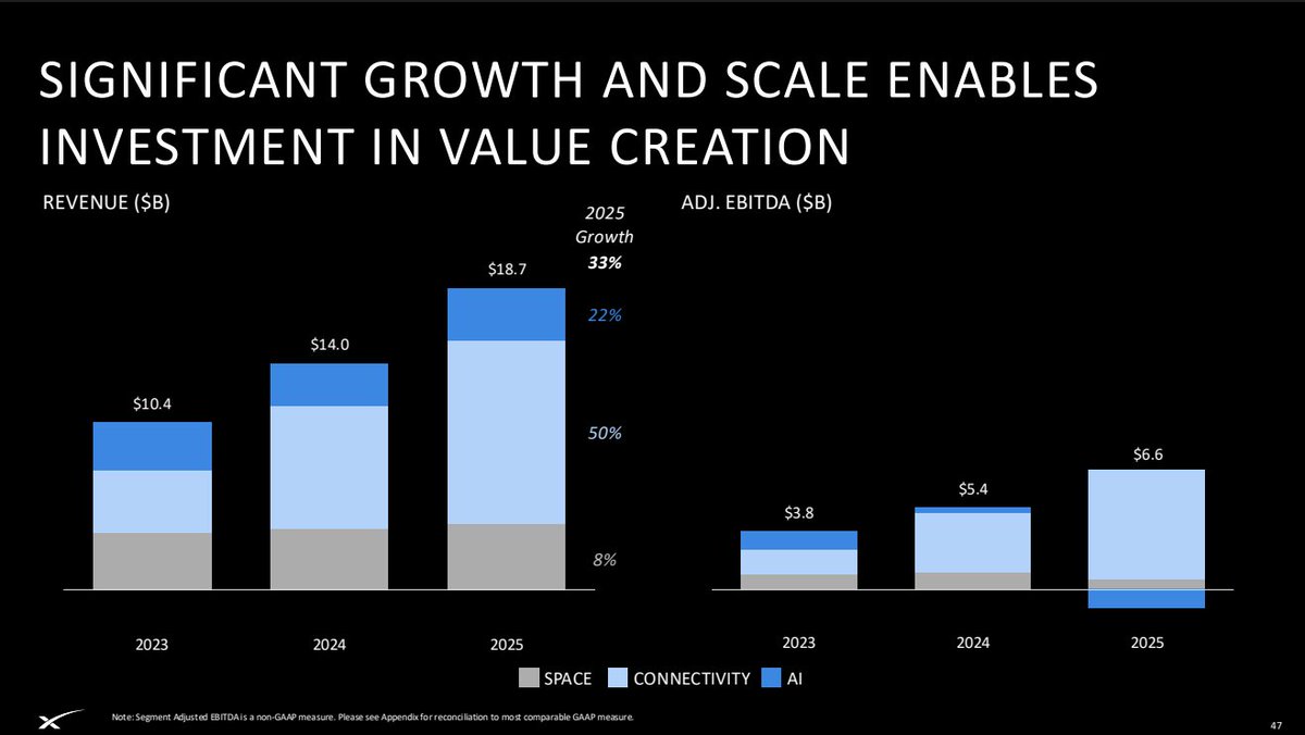
$SPCX - SPACEX IPO: THE BIGGEST BET IN MARKET HISTORY
SpaceX is really three businesses under one stock:
Starlink is the profit engine, generating $11.4B in revenue and $4.4B in operating profit in 2025. Subscribers grew from 2.3M in 2023 to over 10M by early 2026.
SpaceX Launches generated $4.1B in revenue but lost money due to massive investment in Starship, the rocket intended to dramatically lower launch costs.
AI (xAI X) generated $3.2B in revenue but lost $6.4B in 2025, consuming all of Starlink's profits and more.
Without AI, SpaceX was profitable. With AI, it lost nearly $5B in 2025 and another $4.3B in Q1 2026 alone.
The IPO values SpaceX at $1.77 trillion, but only 4.3% of shares will trade initially. That limited float could drive strong early demand and volatility while making true price discovery difficult.
Retail investors are getting access to just 1.3% of the company, while insiders and major funds remain largely locked up. Those restrictions begin easing within months, potentially increasing selling pressure.
SpaceX will not immediately join the S&P 500, as it currently fails key inclusion requirements, delaying an estimated $14B of passive index-fund buying.
The biggest risk is valuation. At roughly 90x sales, SpaceX is trading at a premium far above the largest technology companies. Historical IPO research shows that highly valued, low-float, unprofitable IPOs often deliver strong first-day gains but weaker long-term returns.
The bullish case is simple: SpaceX dominates satellite internet and commercial launches, and Starship could reshape the economics of space. The bearish case is that investors are paying an unprecedented price today for profits that may arrive years from now.
Bottom line: SpaceX may become one of the most important companies of the century. But this IPO looks designed to maximize demand in the short term, while much of the future selling pressure arrives later. For retail investors, the excitement is obvious—the risk is whether today's valuation already prices in most of the future success.
126
179
1,267
315,116
Jun 12
多说一句,关于晶圆有很多种分类方式,比较常见的一种是按照功能来分:
1️⃣逻辑晶圆 logic wafers,
2️⃣内存晶圆 memory wafers,
3️⃣模拟与功率晶圆 analog /power wafers,
4️⃣图像传感 CIS wafers
1
7
4,739
Jun 12
逻辑晶圆主要供应商:
1️⃣台积电 $TSMC:全球最大晶圆代工厂,逻辑为核心业务,覆盖 7/5/3/2 nm 等先进制程到 28 nm 以上成熟节点,
2️⃣三星半导体(Samsung Foundry):兼具存储与逻辑的 IDM/Foundry,提供从 3 nm GAA 到成熟节点的逻辑晶圆代工服务,是仅次于台积电的高端逻辑晶圆供应商之一。
3️⃣Intel:传统 IDM,自用逻辑晶圆为主,同时扩大对外代工(IFS),在高性能 CPU、数据中心逻辑晶圆上也是重要供应者
Jun 11

$MRVL Marvell CEO Matt Murphy: “There's still not enough logic wafers to go around.”
2
1
11
9,477

Jun 11
说着最狠的话,干着最软的事。
如果没记错,这是特朗普第38次说快要达成协议和开放海峡。
Jun 11
特朗普:今晚将严厉打击伊朗,并在某个时候夺取哈尔克岛。
不懂就问,这个岛夺下来的可能性高么?
5
15
9,178
Jun 11
谷歌据悉正与三星洽谈 共同研发下一代芯片
谷歌正与三星洽谈,拟采用三星2nm工艺制造其下一代TPU(代号“Icefish”)的部分组件。
3
13
7,147
Jun 11
老师对学生说:“你要是不好好读书,以后就在车间拧螺丝。”
10年后,高中毕业的学生在SPACEX拧螺丝,即将因为IPO财富自由。
24
4
337
38,586