
Courage is contagious. Go spread it. Producer @SquawkStreet @SquawkAlley @CNBC. @sajahq Board Member x-@AJAM @FortuneMagazine @BloombergTVInd @Citi
Joined June 2009
- Tweets 11,344
- Following 1,557
- Followers 3,383
- Likes 14,215
752 Photos and videos


Pinned Tweet

15 Apr 2021
So excited to be part of this!!
@Work_bench kudos on bringing together this event which can now be a virtual learning experience for anyone interested in the #Enterprise tech #software ecosystem!
Have specific Qs for @digitalocean's @yanceyspruill?
I'm all ears!
15 Apr 2021

So excited to have @CNBC's @sameepa join us next Wed to moderate our #NYETM with @digitalocean's @yanceyspruill🔥
It's gonna be a great convo on winning the ❤️s of developers, competing in the crowded ☁️ environment, top lessons for enterprise founders, & more!
4
2
22
Sameepa Shetty retweeted

Jun 13
As a result of a US government directive, we are suspending access to Claude Fable 5 for all users. You can continue to use all other Claude models.
Here’s what this means for you:
Across Claude products, new sessions will run on your selected default model or Opus 4.8, and existing Fable 5 sessions will end with an error.
On the Claude Platform, requests to Fable 5 will also return an error. Please update your integrations to other Claude models.
We know this is a disruption to your workflows; we appreciate your patience and support.
Jun 13

The US government, citing national security authorities, has issued an export control directive to suspend all access to Fable 5 and Mythos 5 by any foreign national, whether inside or outside the United States, including foreign national Anthropic employees.
The net effect of this order is that we must abruptly disable Fable 5 and Mythos 5 for all our customers to ensure compliance.
Access to all other Claude models is not affected.
We apologize for this disruption to our customers. We believe this is a misunderstanding and are working to restore access as soon as possible.
Read our full statement: anthropic.com/news/fable-myt…
3,665
7,272
44,651
12,883,154
Sameepa Shetty retweeted

Manhattanhenge on 42nd Street, Times Square in New York City
Summer 2026 Dates
May 28 at 8:14 PM ET: Half Sun on the Grid
May 29 at 8:13 PM ET: Full Sun on the Grid
July 11 at 8:20 PM ET: Full Sun on the Grid
July 12 at 8:21 PM ET: Half Sun on the Grid
68
1,271
11,176
884,741
Sameepa Shetty retweeted

May 7
The most female-led product org in tech right now:
Chief Product Officer: Ami Vora
Claude Code/Cowork Head of Product: Cat Wu
Claude Code/Cowork Head of Eng: Fiona Fung
Claude Platform Head of Product: Angela Jiang
Claude Platform Head of Eng: Katelyn Lesse
Research Head of Product: Dianne Penn
President: Daniela Amodei
(Also, the fastest-growing company in history)
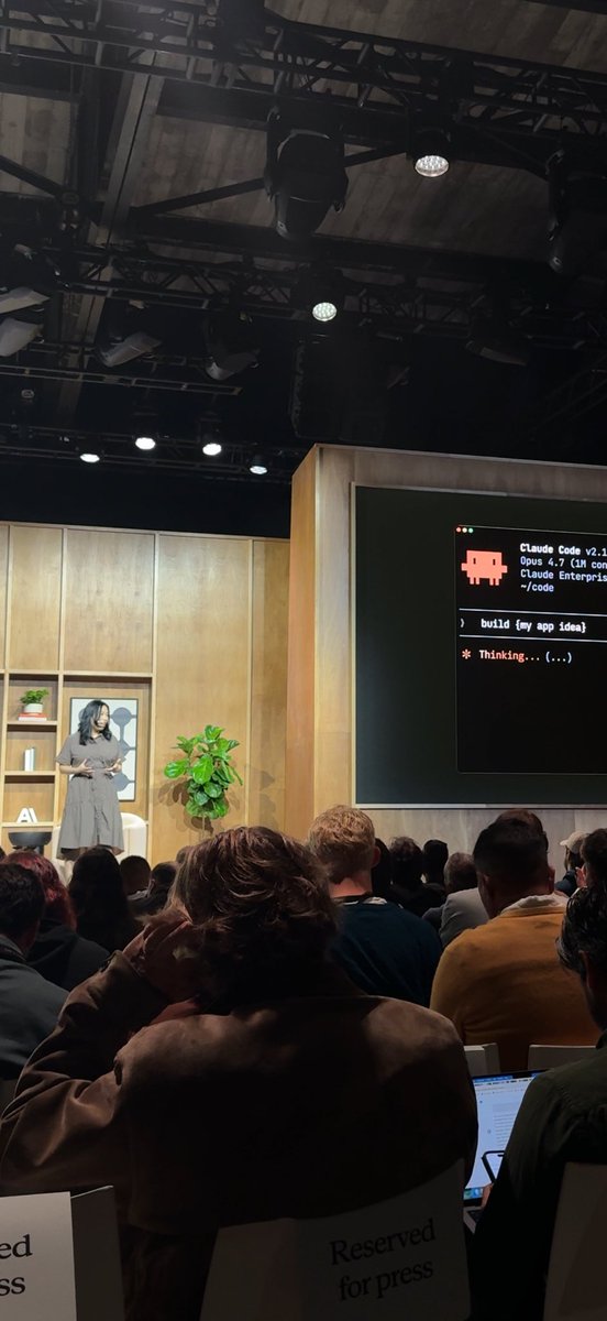
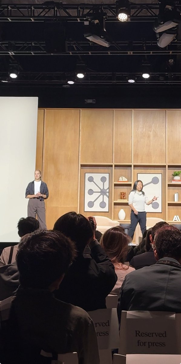
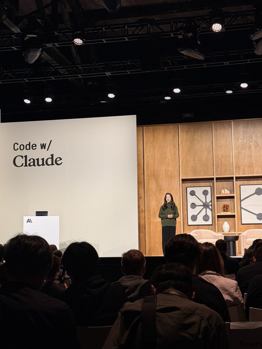
May 6

30 mins into the claude code keynote and every speaker so far has been a woman. just saying 🫶🏻
@asvora @angjiang @katelyn_lesse @_catwu Dianne Penn @claudeai
113
487
4,213
511,264

Effective today, we are:
1) Doubling Claude Code’s 5-hour rate limits for Pro, Max, and Team plans;
2) Removing the peak hours limit reduction on Claude Code for Pro and Max plans; and
3) Substantially raising our API rate limits for Opus models.
1,243
3,930
44,454
9,114,566
Sameepa Shetty retweeted

May 1
Useful.

10
28
499
232,174
Sameepa Shetty retweeted

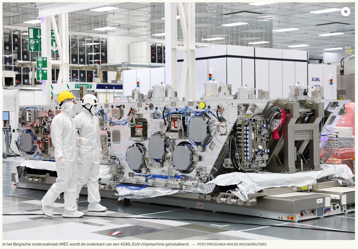
The ASML book author saw the next generation – Lace Lithography, using helium atoms shooting through a holographic mask to scale beyond what’s possible with light, where the wavelength is larger than atomic scale.
“ASML is the only company capable of using EUV—extreme ultraviolet light—to print ultra-fine chip patterns at the 2-nanometer level desired by Musk. Last year, ASML produced 48 of these EUV machines. While there are plans to ramp up production, a rapid doubling of output is not in the cards—ASML’s suppliers simply cannot manage that pace.”
“Lace Lithography is developing a lithography machine capable of printing chip circuitry using helium atoms. ‘Where light ends, atoms begin,’ says Bodil Holst, founder of this start-up based in Bergen, Norway. The wavelength of light determines the precision with which one can 'print.' Think of it like making a tiny drawing: you would much rather use a fine-tipped pen than a blunt carpenter's pencil. EUV employs a wavelength of 13.5 nanometers and further narrows that beam using mirrors. The 'beam' of helium atoms, however, is less than one-tenth of a nanometer wide, allowing it to draw with far greater intricacy.”
“In a nutshell: Lace propels energized helium atoms—each carrying an extra electrical charge—through a mask perforated with tiny holes. The atoms that pass through unimpeded strike the photosensitive layer of a silicon wafer, thereby etching the desired pattern. That perforated mask reminded Bodil Holst of *kantklossen* (known in English as 'lace making'), which is why she named her company just that. A test rig is currently operational at the Lace laboratory in Bergen”
“The foundation for this ‘atomic approach’ dates back to the 1990s, but neither the timing nor the technology was ripe for it at the time. This is because extensive computation is required to design the perforated diffractive mask in such a way that the chip's circuitry remains accurate. This can only be achieved with the aid of AI using high-speed chips—explains Adrià Salvador Palau. ‘Consequently, without the powerful chips made by EUV machines, we would never have been able to solve this problem.’"
— Translated from the Dutch original: nrc.nl/nieuws/2026/04/03/kan…

𝐅⃣𝐎⃣𝐂⃣𝐔⃣𝐒⃣ The ASML Way
I just finished this history of the most important semiconductor equipment company in the world, as translated from the Dutch original (and lurking in the background might be a better way).
Reminder: ASML builds 100% of the world’s extreme ultraviolet (EUV) lithography machines, without which cutting edge chips are simply impossible to make. It’s the most expensive mass-produced machine tool in history. Oh, and today, there are two special women without whom, all EUV lithography would sputter to a stop (see p.141 below)
ASML was formed in 1984 as a JV with Philips, the Dutch electronics company that contributed ~$15M (in guilders) and 40 engineers, and “it seemed doomed from the start.” (p.35) There were 10 viable competitors at the time, more than enough to serve the market as ASML learned at SEMICON in 1984 (by coincidence, I was also there with my Dad who about to leave Mostek to run Varian’s Semiconductor Equipment Group, but they only had Molecular Beam Epitaxy, a low throughput lithography alternative. My Dad’s attempt to poach a CTO from ASML is on p.72).
“In these initial years, management worked around the clock to bring in new subsidies. In these initial years, about half of ASML’s money for research came from The Hague or Brussels.” (48)
ASML’s “machines were the first in the industry to utilize modular design. The lens, the wafer-table, the frame for the mask, the light source, the robot that picks the wafers: these are LEGO blocks that, when you bring them together, form a lithography system.” (62)
IPO in 1995. Stock went up 600x in the 30 years that followed. March 2000 market crash: “cancellations from chip manufacturers poured in daily. On paper, the company was bankrupt. Radical cost-cutting measures would be needed.” (82)
Nikon sues: “a rude awakening. ASML had paid far too little attention to its intellectual property in its early years.” (98) “The best inventors, some of which have more than 200 patents to their name, are commemorated by having their faces engraved on silicon wafers and hung on a series of large wooden beams, like a Mount Rushmore of the chip industry. As of 2023, ASML has registered more than 16,000 patents.” (99)
The machines are insanely sensitive. “Atmospheric pressure fluctuations due to thunderstorms can easily disrupt the lithography process. Or cows. Intel once faced an inexplicable drop in yield every night for a few hours, with researchers running in circles until they finally realized the cause: cow farts. Intel had to pay for three farms to relocate.” (117)
“In 2006 Intel, who was supplying the chips for Apple’s computers, was asked if it could also supply the processor for the iPhone. It declined.” (122)
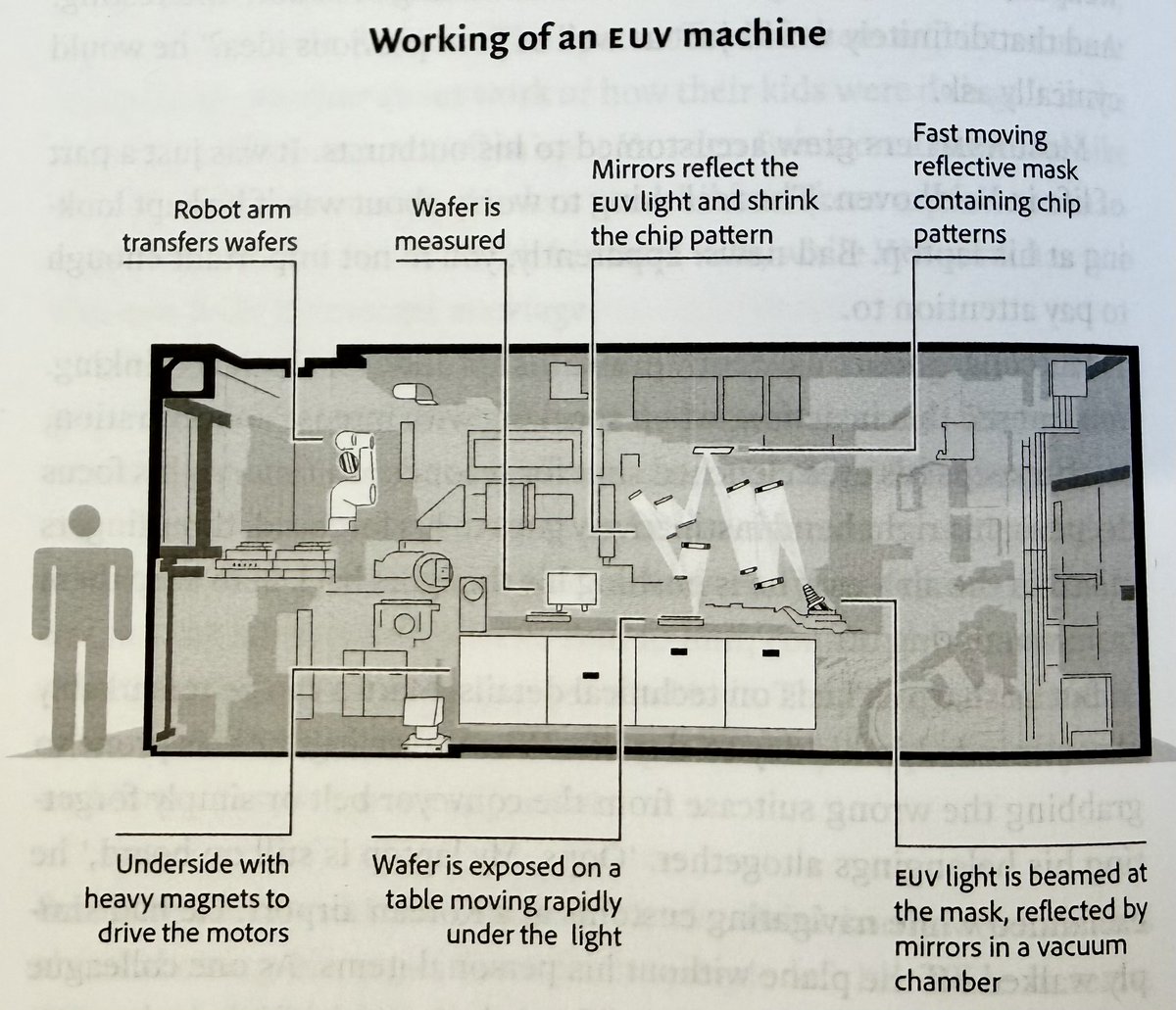
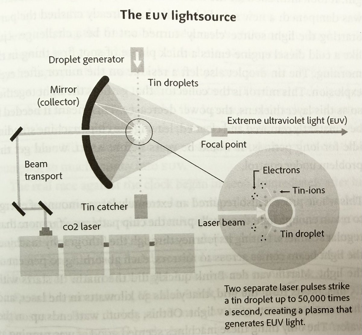
“EUV light is extremely difficult to generate and sustain in an industrial environment. The invisible rays are absorbed by almost all materials, even the air, which means the lithography machine needs to have (curved, atomically precise) mirrors instead of lenses and can only operate in a vacuum.” (127)
The Cymer laser / light source has a molten tin “droplet generator capable of forming a 30-micron droplet of tin at a rate of 50,000 times per second. The laser was rigged to deal two separate blows. First, a gentle tap to flatten the droplet into a pancake-like shape, followed by an intense blast that heated the tin to 200,000 degrees, transforming it into a plasma.” (130)
“During its journey through the lithography machine, the light beam comes across 10 mirrors, each absorbing 30% of the light. It starts with 1.5 megawatts from the grid that yields 30 kilowatts in the laser, and that creates 100 watts of EUV light. Of this, about 1 watt ends up on the wafer. But more power also creates more heat. That causes the mirrors to expand, which in turn causes small deviations that immediately need to be corrected with small motors. Even the EUV mask, which carries the blueprint of the chip on it, is itself an extremely sensitive mirror.” (132)
“ASML was vastly underestimating the financial consequences of the new technology. In retrospect, this was for the best. No respectable CEO would sign for a project that would take 20 years, without any promise of success or interim profit to carry it through. That’s not taking a bet, that’s bananas. This is also why the Japanese competition dropped out of the race: not because their engineers were any less capable, but because Nikon and Canon were simply not prepared to continue pumping so much money into EUV.” (133)
To finance the purchase of Cymer in 2012, “Intel invested 3.3B Euros into ASML in exchange for 15% of the shares. TSMC was required to purchase 5%... and Samsung acquired a stake at the 11th hour, taking 3%.” (139)
“Only Joann and one of her colleagues have the ability to wind and solder invisibly small wires (around the nozzle that shoots the tin droplets). It’s a delicate task few could ever master. ‘Even watchmakers can’t do this,’ says their awestruck boss, ‘and there’s no way to automate it.’ It’s not a trivial matter: the nozzle regularly gets clogged during day-to-day use in the chip factory. When that inevitably happens, the only thing to do is to swap it out for a new one. It’s hard to imagine, but without the fingers of Joann and her colleague, the EUV machines at Samsung and TSMC would grind to a halt.” (141)
In 2013, “most of the droplet generator was still hand-made by Cymer, and it was virtually impossible to test the part in advance. This made for completely unpredictable yields: in the initial phase of production, half of the droplet generators didn’t even work.” (142)
“20% of the South Korean economy now relies on the revenue of one single company. Hence their nickname: this is the republic of Samsung.” (156)
“Intel was being surpassed by their competitors in Asia on every front and would only start using EUV for chips after 2023.” (160)
“The descriptions that chip manufacturers use for these technological generations or ‘nodes’ need to be taken with a grain of salt. The physical dimensions of the smallest circuits and connections on the chip are, in practice, 5 to 10 times larger than advertised. A nanometer was once a nanometer, but accuracy has never stopped a good marketing slogan.” (161)
Cousins “Lisa Su and Jensen Huang, the leaders of AMD and NVIDIA were both born in Tainan, the city where TSMC now produces their chips.” (164)
“The culture at TSMC is more hierarchical than ASML, but less militaristic than in South Korea.” (166)
“TSMC now commands 60% of the entire foundry market, making it 4x larger than its closest competitor, Samsung.” (167)
“ASML’s next generation of EUV machines goes by the nickname High NA (the numerical aperture increases from 0.35 to 0.55). These colossal scanners span 14 meters and feature large mirrors up to a meter wide. The optical system by itself consists of 20,000 parts and weighs 12 tons, making it 7x heavier than the optics for the current EUV machine.” (175)
“The High NA system weighs 150 tons and costs 400M Euros. It takes 7 cargo planes to ship this system to customers.” (225)
“The production of a complex EUV mask costs more than a half million Euros and takes a huge amount of time to calculate.” (181) They “use AI to understand the interplay between the light beam, the mask, and the chemical reactions on the wafer.” ASML’s CTO calls it “voodoo software.” (183)
China: “European governments fear China is transforming into a totalitarian state, capable of forcing Chinese multinationals to spy for the Communist Party. And that poses significant risk to the 5G cellular infrastructure of the West.” (200)
“In 2017, Chinese customers ordered 700M Euros worth of lithography machines, a new record. Hundreds of ASML’s scanners were running in the factories of SMIC, China’s largest foundry” (201)
“EUV is controlled by the Wassenaar Arrangement, the multilateral export control regime on conventional arms and dual-use goods and technologies.” (203)
“As far as ASML is concerned, fears about EUV being used for military applications are baloney. Most chips found in weapons are ‘off-the-shelf’ chips that can also be found in laptops, washing machines or cars, and are easy to purchase anywhere in the world. But the U.S. sees things differently. They fear the emergence of Chinese AI and cyber weapons. And there is one thing those all need: advanced chips.” (205)
“In January 2020, the U.S. asked the Netherlands to block EUV exports, and suddenly ASML found itself in the spotlight. The Netherlands ultimately denied ASML a license… No EUV machine was going to SMIC.” (208)
In 2023 “ASML was exporting far more older DUV machines to China than had been expected. Almost half of ASML’s revenue was coming from China. As the chip industry was pushing the pause button, China kept on hoarding. The U.S. pressed the Netherlands to slam the brakes before January 2024, and the cabinet duly revoked several approved export licenses for ASML machines destined for China.” (234)
“As China is growing increasingly isolated, so too is the liklihood of a fully-fledged Chinese competitor emerging in the rearview mirror capable of developing an independent chip production chain.” (236) “ASML takes this seriously. Their go-to response: ‘The laws of nature are the same anywhere.’ What was achieved in Brabant, could be achieved in Beijing.” (335)
“To qualify for government aid (in Biden’s Chips Act), companies had to agree not to build advanced chip foundries in China or other ‘countries of concern.’” (239)
“The chip shortage had been a wakeup call, and the nightmare scenario was front and center on everyone’s mind: if China blocks Taiwan, we’ll be without chips within two weeks.” (242)
“The estimated percentage of people with autism or ADHD at ASML far outnumbers the average. The highly specialized work, revolving around focusing on complex problems that require prolonged attention to the smallest details, makes it well-suited for some autistic traits. ASML’s CTO and President Van den Brink makes no secret about being dyslexic and actively advocates for targeting this neurodiverse group. They are precisely the analytical and creative thinkers ASML needs, but also often the ones who find it difficult to put themselves in other people’s shoes.” (287)
Sounds like teen spirit… of Steve Jobs: “Van den Brink’s power of persuasion lies in his childlike enthusiasm. It works like some kind of reality distortion field. Martin can disrupt your perspective until you’re convinced that you can make the impossible possible.” (321)
“Van den Brink never really led a big company. He guided it like a startup, as if it were a defiant toddler in the body of a mature multinational.” (329)
The book ends with the poignant handover of the company in 2024 to a new leader, the Frenchman Chistophe Fouquet.

23
174
1,157
125,454
Mar 18
Anthropic Just Did What OpenAI and Google Haven't. And It's More Significant Than the Headline Suggests. linkedin.com/pulse/anthropic…
74
Mar 16
Check out my latest article: Translating the Invisible Race: 5 Ways Apple TV Can Revolutionize F1 Storytelling for the 2026 Era linkedin.com/pulse/translati… via @LinkedIn
110
Sameepa Shetty retweeted

Mar 12
4
21
163
14,015
Mar 1
.@IndiGo6E NO response on PNR:O4J57F. Left pouch w/ ₹1 LAKH cash & docs in Seat 11B, 6E865 (Navi-IXE) Feb 27. Need urgent CCTV & cleaning crew audit. Disappointing ground support. Escalating to @AirSewa @MoCA_GoI @Mangalore_Arprt @JM_Scindia if no update NOW. #IndiGo #Travel
4
767
Sameepa Shetty retweeted

15 Jul 2025
In it’s heyday, Goldman’s special situations group was the navy SEALs of money making. Today’s guest, Alan Waxman, used to run that group before leaving to build Sixth Street, now a $115b behemoth.
SSG heads were sometimes of the more brainy, nerdy variety. Not Waxman. He is a force of nature and energy who apparently would pound around the SSG office, loudly and enthusiastically asking people “who is going to make us some money today?!”
When I asked another SSG alum about Alan, he said his main memory was his remarkable nose for talent. Once, the smartest guy at SSG (which is saying something) was a mere entry level associate, 6 or 7 rungs in the hierarchy below Waxman. But, Waxman immediately recognized the raw talent and was joined to this associate at the hip.
Under Waxman and his team, SSG produced an insane (so insane I can’t quote it!) percent of Goldman’s bottom line. In creating Sixth Street with his partners and team, he sought to recreate and expand the magic of the SSG days. Here, in his first interview of this type, he shares the entire story.
I found Alan to be a singular force. His team is ridiculously talented, and nobody leaves (they’ve never lost a senior person). They’ve even built a unique pool of capital called Tao that sits atop the rest of the firm…tens of billions that can go anywhere and do anything as a permanent pool of money with no restrictions, other than to earn the highest risk adjusted returns possible. Sounds a lot like SSG.
This was one of my favorite conversations this year. I hope you enjoy. Face the tiger!
Timestamps
0:00 Intro
0:38 The Formative Goldman Sachs Experience
5:58 Unitizing Risk and Return
10:09 Facing the Tiger: Culture and Values
24:55 The Genesis of Sixth Street
34:09 Spotify and Airbnb Investments
37:52 The Flexibility of TAO
41:42 COVID-19: Playing Offense
44:42 Analyzing Risk and Business Models
48:35 Investing in Sports and Live Experiences
54:44 Developing Investment Themes
58:16 Personal Development and Firm Culture
1:19:00 The Future of Sixth Street
1:21:52 The Kindest Thing
74
242
3,371
768,773
Sameepa Shetty retweeted

19 Jun 2025
Andrej Karpathy's (@karpathy) keynote yesterday at AI Startup School in San Francisco.
136
1,220
6,318
2,133,337
Sameepa Shetty retweeted

1 Jun 2025
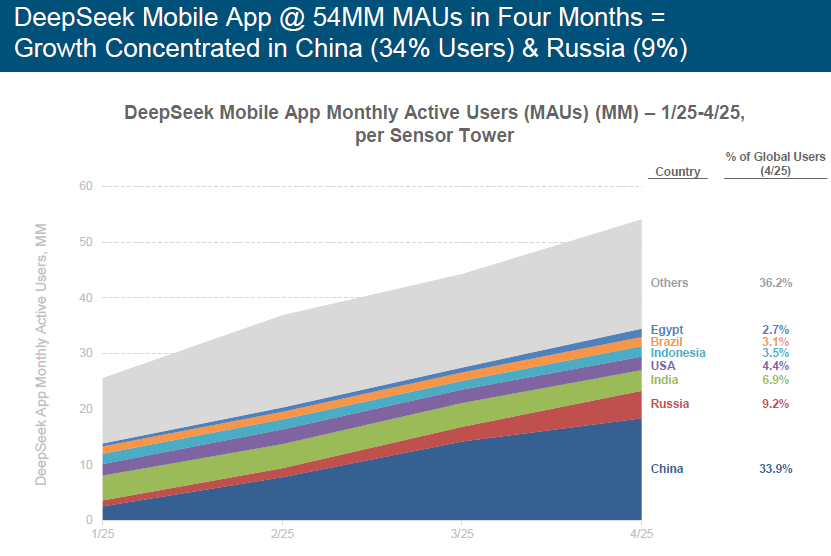
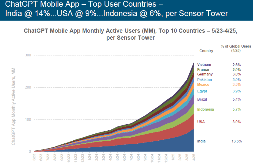
India's AI usage --"Jai Jio" 🇮🇳
(a) India is the 2nd largest market for OpenAI’s ChatGPT app 🤯
13.5% of global users of ChatGPT’s mobile app come from India
(b) And, more surprising, India is the largest “opt-in” market to DeepSeek 🤯
7% of global users of DeepSeek’s mobile app come from India
Note: Russia & China restrict OpenAI ChatGPT usage, hence, India is an “opt-in” country
(c) This is a “Jai Jio” moment more than anything else → lower cost per GB internet data has brought 67% of the country online.
5
33
191
81,776
13 May 2025
"Publishers will be able to choose from over 100 AI-generated voices in English, Spanish, Italian, and French."

Audible is giving publishers AI tools to quickly make more audiobooks theverge.com/news/666136/ama…
156
Sameepa Shetty retweeted

8 May 2025
AI is eating financial research.
7 May 2025

Perplexity Finance is a companion for live earnings. We extract headline metrics, display live call transcripts, and synthesize insights during earnings calls -- all faster than you can find elsewhere.

31
70
999
141,086
Sameepa Shetty retweeted

30 Apr 2025
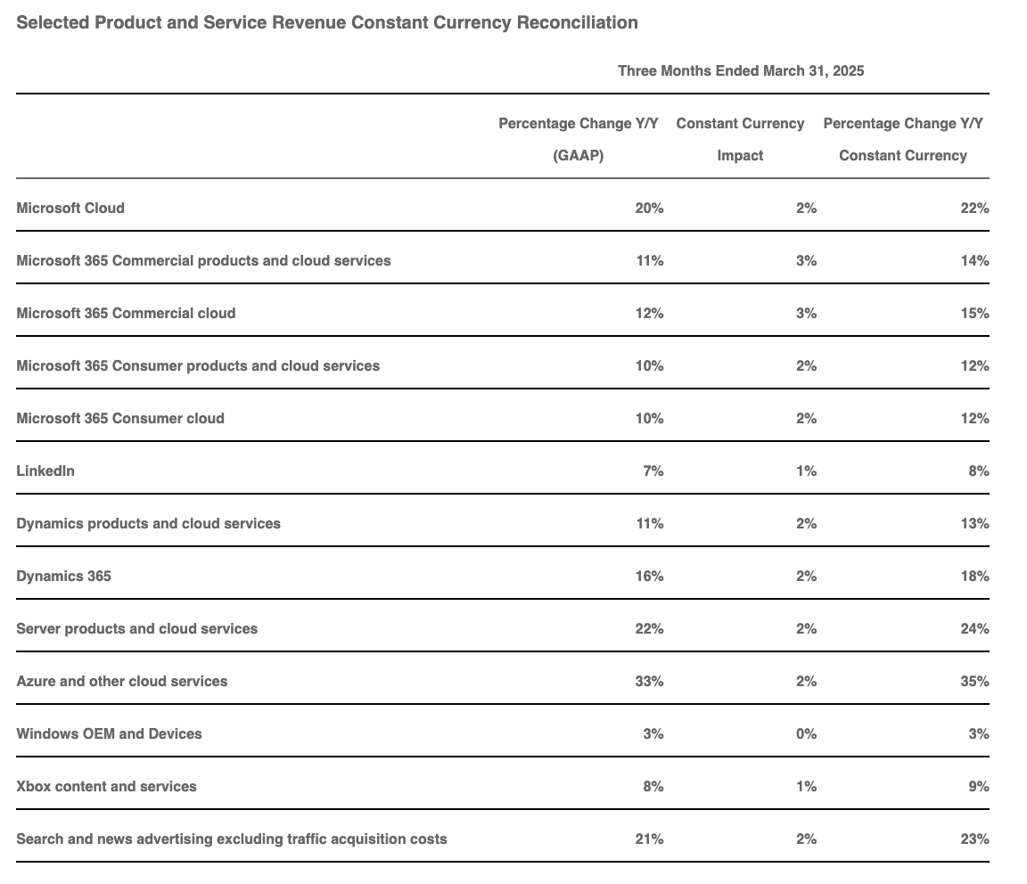
$MSFT Microsoft Q3 FY25 revenue growth by product line [Constant Currency YoY]
—Microsoft Cloud: 22%
—Azure & other cloud services: 35%
—Server products & cloud services: 24%
—Microsoft 365 Commercial: 15%
—Microsoft 365 Consumer: 12%
—Dynamics 365: 18%
—LinkedIn: 8%
—Xbox content & services: 9%
—Search & news ads (ex-TAC): 23%
—Windows OEM & Devices: 3%
28
24
134
19,412
Sameepa Shetty retweeted
30 Apr 2025
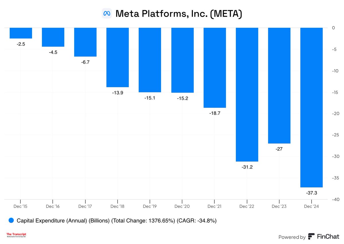
$META CFO hikes their capex guidance for FY 25:
"We anticipate our full year 2025 capital expenditures, including principal payments on finance leases, will be in the range of $64-72 billion, increased from our prior outlook of $60-65 billion"
10
9
71
7,795
Sameepa Shetty retweeted

23 Apr 2025
The share of equities held by people who are at or near retirement age (55 ) has climbed to about 80%, up from 60% two decades ago, according to an analysis of Federal Reserve data by Rosenberg Research.
Read more: unusualwhales.com/news/indiv…
27
17
120
102,497
Sameepa Shetty retweeted
22 Apr 2025
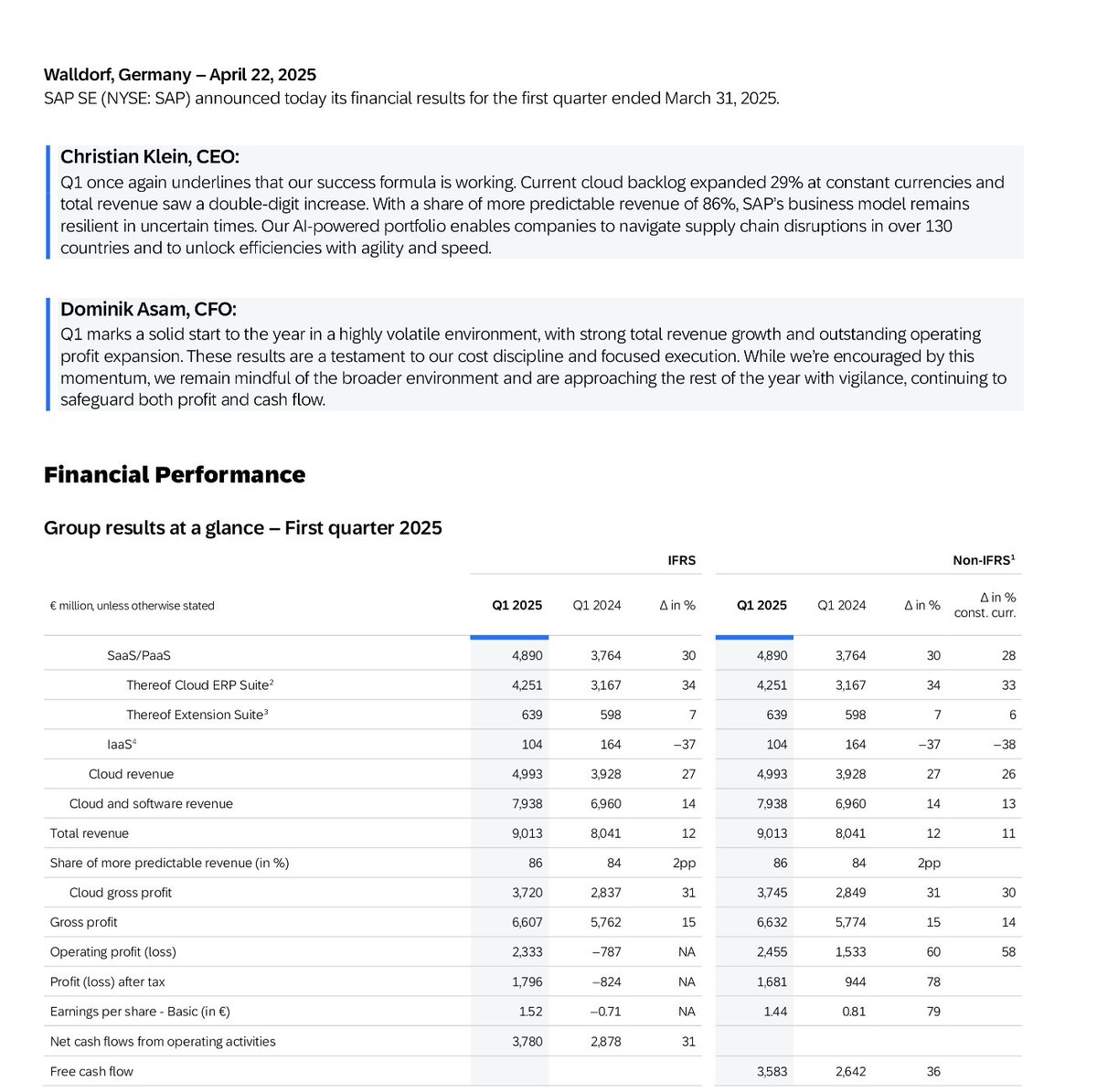
$SAP
CEO: "With a share of more predictable revenue of 86%, SAP’s business model remains resilient in uncertain times"
CFO: "Q1 marks a solid start to the year in a highly volatile environment."

10
9
50
8,068