
Substrate is building America's next-generation semiconductor foundry
Joined May 2022
- Tweets 12
- Following 0
- Followers 12,752
- Likes 27
3 Photos and videos


Pinned Tweet

Apr 7
Over the past few months, we have integrated @googledeepmind's AlphaEvolve into our computational lithography. Enabled by AlphaEvolve's algorithmic leaps, we are now printing complex patterns in a single exposure that would otherwise require multiple. substrate.com/information-to…
11
83
665
220,741
Substrate retweeted

May 7
Congratulations to the @googledeepmind team. @jeffdean's work on "TPU brains helping design next-generation TPU bodies" is a powerful demonstration of where AI co-design is heading in semiconductors.
May 7

We are honored to see our work with @googledeepmind's AlphaEvolve featured alongside major breakthroughs from @googleresearch and @googlecloud, as well as other impactful commercial applications.
4
11
50
18,470
May 7
We are honored to see our work with @googledeepmind's AlphaEvolve featured alongside major breakthroughs from @googleresearch and @googlecloud, as well as other impactful commercial applications.

Algorithms are part of nearly every aspect of life, from the physics of the natural world to planning shipping routes.
Our Gemini-powered coding agent AlphaEvolve has been accelerating progress over the last year - from quantum and biotechnology to logistics and @Google’s AI infrastructure. ↓ goo.gle/4uzfe0C
2
10
48
27,475
Apr 7
Over the past few months, we have integrated @googledeepmind's AlphaEvolve into our computational lithography. Enabled by AlphaEvolve's algorithmic leaps, we are now printing complex patterns in a single exposure that would otherwise require multiple. substrate.com/information-to…
11
83
665
220,741
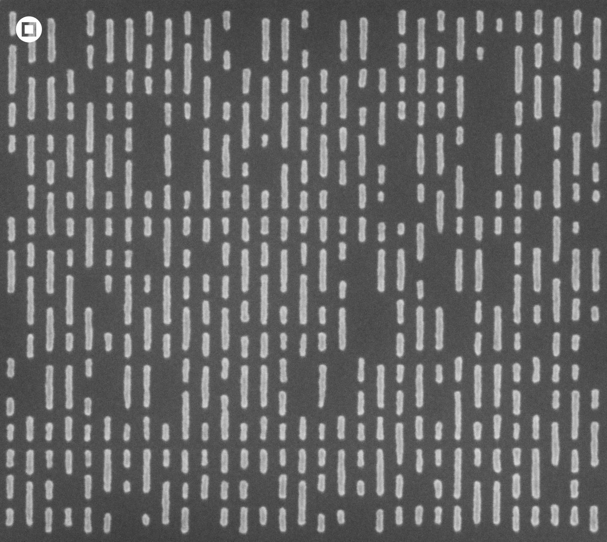
Apr 7
A metal one (M1) layer, first simulated by AlphaEvolve-optimized models and then printed in a single exposure with our X-ray lithography tool at a 12 nm half-pitch, resolution equivalent to the 2 nm node. The M1 layer is the most demanding of an advanced semiconductor device.
ALT Printed P24 M1 (12 nm CD) with measurements from a scanning electron microscope.
1
7
105
9,871
Substrate retweeted
18 Dec 2025
In September 2023, the @substrate team prepared an analysis on China's (still) not-yet-known rapid progress in advanced precision optics for EUV. This important work by China might otherwise be missed. We redacted portions we deemed best to protect. substrate.com/optics_documen…
3
5
32
6,055
Substrate retweeted
18 Dec 2025
Yesterday, @Reuters reported that China had completed a domestically built EUV tool. In the piece, they stated that "China still faces major technical challenges, particularly in replicating the precision optical systems that Western suppliers produce." reuters.com/world/china/how-…
6
22
80
20,811
Substrate retweeted

30 Oct 2025
10-30-2025 ($)
An Interview with Substrate CEO James Proud About Building a Disruptive Foundry in America
stratechery.com/2025/an-inte…
1
6
39
36,018
Substrate retweeted

29 Oct 2025
How to Kill 2 Monopolies with 1 Tool
Substrate X-Ray Lithography,
a New American Foundry,
$10k Logic Wafers
newsletter.semianalysis.com/…

23
76
614
407,334
Substrate retweeted
28 Oct 2025
History repeatedly shows that American science and engineering solve impossible tasks. I started Substrate because I believed that this impossible task is one worth trying.
28 Oct 2025
Substrate is building a next-generation foundry to return America to dominance in semiconductor production. To achieve this, we will use our technology—a new form of advanced X-ray lithography—to power them.
America invented semiconductors. We will lead again.
105
205
3,291
398,220
28 Oct 2025
Substrate is building a next-generation foundry to return America to dominance in semiconductor production. To achieve this, we will use our technology—a new form of advanced X-ray lithography—to power them.
America invented semiconductors. We will lead again.
151
486
4,968
1,501,241
28 Oct 2025
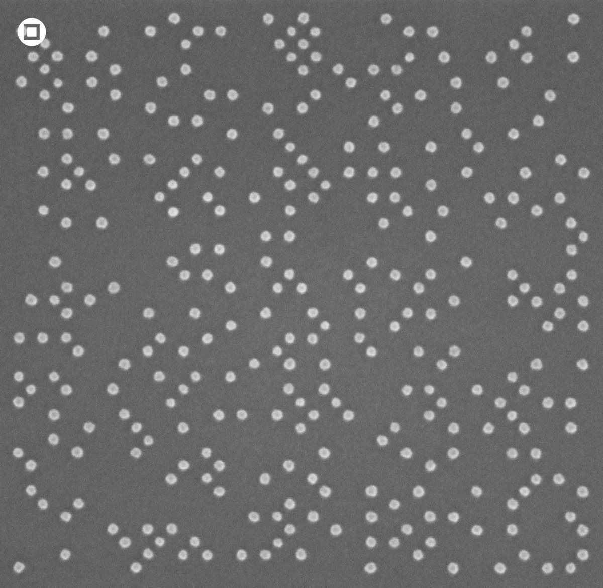
These patterns have been printed using a Substrate lithography system with no IP or supply chain input from other advanced lithography tools.
The resolution of the features in these images is equivalent to that achievable only with what the semiconductor industry refers to as “High NA EUV lithography” and matches features printed at the 2 nm semiconductor node and below.
All of these images were printed in a single exposure, with no multi-patterning.
99
224
3,681
1,577,616
28 Oct 2025
The United States invented all of the critical technologies that power today’s advanced semiconductors, but over time, we have lost the lead.
For years, many have spoken of the need for a new pure-play American foundry, yet view it as an impossible task. History repeatedly shows that American science and engineering solve impossible tasks. As we rush to build more current-generation semiconductor fabs in America today, we need to start immediate work on building the semiconductor fabs of tomorrow.
The stakes are too high for the United States not to try everything we can to solve both one of our most significant technological gaps and our biggest opportunities to reclaim leadership over the technologies we pioneered.
substrate.com/our-purpose
26
46
1,329
130,353