
Augmented Reality PCB Tools. Interact with hardware like never before.
Joined January 2019
- Tweets 2,127
- Following 1,178
- Followers 1,600
- Likes 7,865
631 Photos and videos


Pinned Tweet

10 Jun 2020
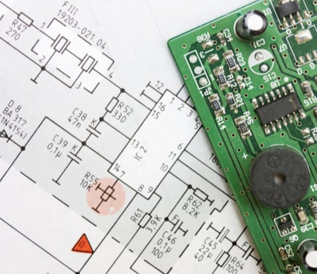
Using inspectAR's overlays, you never have to worry about finding the right pin or trace ever again.
Download today for free - inspectar.com/sign-up-free
#electronics #electrical #electricalengineering #engineering #engineer #hardware #hardwareengineer #firmware #AugmentedReality
1
21
42
2 Aug 2023
Signal reflection and distortion in PCBs are two signal integrity issues that can impact reliability. Learn more here! bit.ly/3XZoSdU
106
26 Jul 2023
Before you manufacture your board you should always simulate its performance. Watch how PSpice can be used to Configure waveform and plot settings to match your requirements when evaluating a circuit’s performance.
#waveforms #PSpice #Cadence
1
167
20 Jul 2023
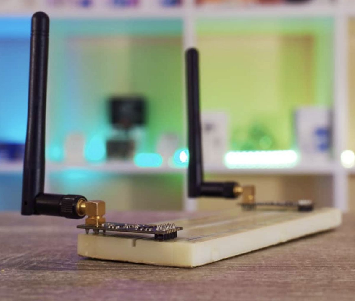
Antenna isolation measurements are significant in reducing the engineering time required to introduce antennas into a system design. bit.ly/46WvPAA
#antenna #cadence #PCBdesign
117
24 May 2023
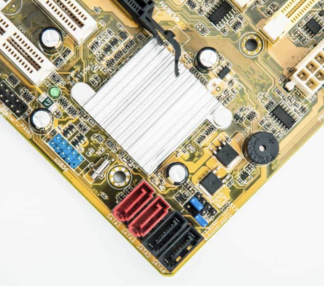
PCB layout considerations are sometimes beyond the designer’s control - communication with the engineer and manufacturing manager is key. bit.ly/3VVWubr
#PCBlayout #cadence
1
120
18 May 2023
Huray surface roughness models are instrumental in describing the attenuation and dispersion of transmitted signals over PCB interconnects. bit.ly/3VY8dX8
#PCBdesign
1
154
12 May 2023
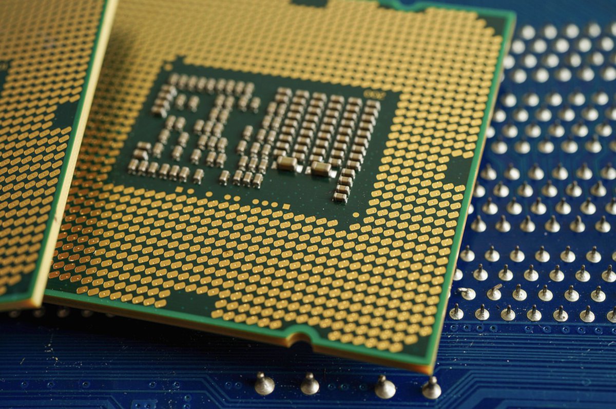
Semiconductor packaging has come a long way ever since planar processes were devices for chip fabrication. In this article, we’ll give you an overview of modern packaging options used to build today’s advanced semiconductor products. bit.ly/3I58Wjo
#semiconductor
2
167
28 Apr 2023
If you’re pursuing a career in electronics, then embedded development is one area where you can excel with the right skill set and background. bit.ly/3zklEpV
#electronic #cadence
1
98
26 Apr 2023
If you are just learning how to use ferrite beads, you will surely encounter temperature effects, LC resonance effects, and the DC bias effect. Learn more here bit.ly/3G8lvcL
#PCBdesign #Cadence
94
24 Apr 2023
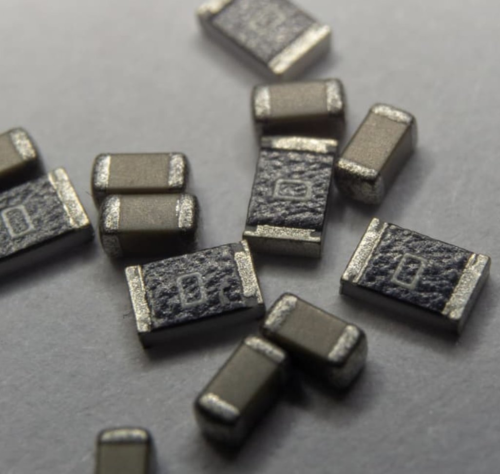
Feeling lost on a dense layout with no ability for a through-hole? Don’t jump to conclusions - use an SMD jumper instead. bit.ly/40OWxXZ
#PCBdesign #Cadence
104
21 Apr 2023
Before you can push your board into production, it’s important to review the surface layers and perform some basic cleanup. Make sure to check for these points in your design before you finalize your board. bit.ly/3M2EUjf
#PCBdsign #Cadence
1
95
19 Apr 2023
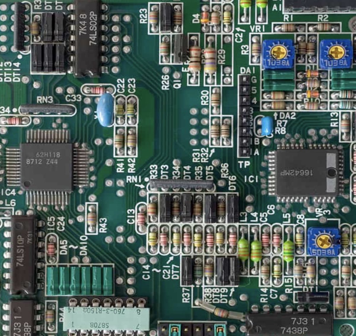
If you’ve ever had signal integrity problems in your circuit board, it could be because the right types of transmission lines weren’t used when laying out the design. bit.ly/3U7wvNp
#inspectAR #Cadence
1
162
17 Apr 2023
4-20mA receiver designs are dependent on the maximum voltage that the receiver can deal with. Learn why in our brief article! bit.ly/42X8wV3
#Cadence #PCBdesign
1
149
14 Apr 2023
PCB design schematics and PCB layout design are two important aspects of any PCB design service. Learn more in our brief article. bit.ly/3zo6OPe
#PCBdesign #inspectar #cadence
1
132
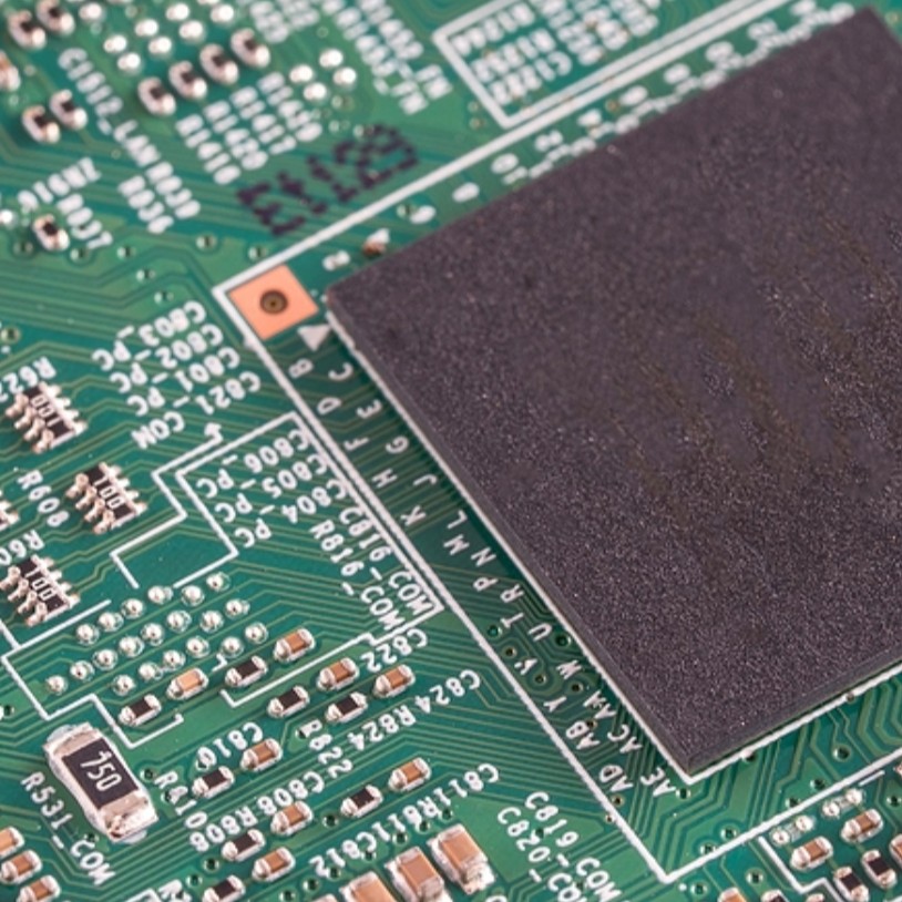
12 Apr 2023
Learn all about circuit routing from an IC, PCB, and signal integrity perspective! bit.ly/40LHuy0
#inspectar #PCB #cadence
1
1
156
10 Apr 2023
Learning how to eliminate clock jitter is important for designers who work on clock trees for digital and analog systems. bit.ly/3G6skeW
#Cadence #PCBdesign
1
3
235
7 Apr 2023
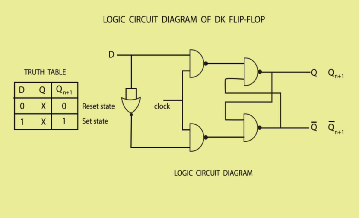
Logic gates are meant to be stepping stones, not barricades. Learn more about logic gates here. bit.ly/3nGLUrG
#Cadence #Logicgates
120
5 Apr 2023
When you think about how to avoid metastability in digital circuits, correlate it with the mean time between failures (MTBF). #Cadence #PCBdesign #electricaldesign #electricalengineer #PCBDesigner #Electronics
1
162
3 Apr 2023
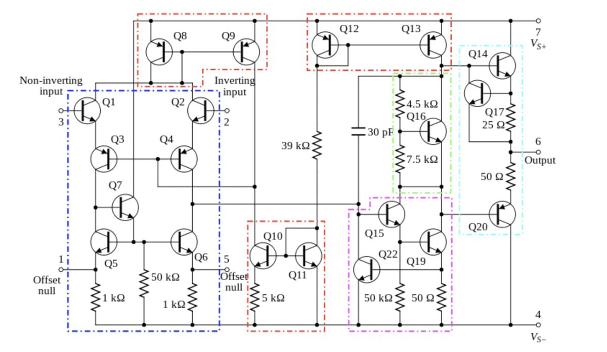
This article covers all the op amp basics, including their construction and various use cases. Learn more bit.ly/3M7JWLj
117
3 Mar 2023
There are many guidelines out there that suggest some bad layout and grounding practices for ADCs. We’ve compiled the important guidelines you need to know in this article. bit.ly/3qTStFQ
#ADC #PCBdesign #Cadence

1
93
1 Mar 2023
Learn the key tools that should be on any electronics laboratory equipment list here. bit.ly/3Vz9xPB
#PCBdesign #electronics #Cadence
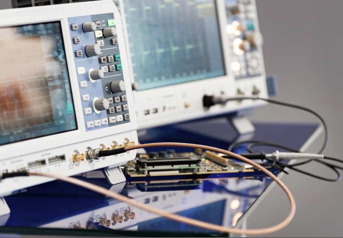
1
89