
May 10
Hands-free wiring made simple with WAGO PUSH-IN CAGE CLAMP® Technology
Experience effortless, secure connections with the WAGO 2624 PCB terminal block.
#WAGO #electronicsengineering #PCB #designengineer #electronics #pcbdesigner #EMS
2
5
329

Mar 25
Kicad V10 added something interesting...
Allegro PCB Import
This is the NXP FRDM-iMX93. All of NXP's design files are Allegro.
#RayPCB #Kicad #nxp #allegro #pcbdesign #pcbdesigner #pcb
2
98
Mar 21
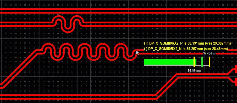
Why Impedance Matching is Critical in High-Speed PCB Design
#RayPCB #PCBdesign #pcblayout #pcbmanufacturing #pcbassembly #engineer #pcbdesigner #electronics #led #hardware #technology

2
53
Mar 14
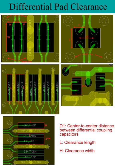
Most PCB engineers control trace impedance carefully. Fewer think about what happens at the pad.
That's where signal integrity problems quietly begin.
In high-speed differential design, your trace impedance might be perfectly tuned — and then the signal hits a pad region. Suddenly:
→ Copper area expands → The pad sits directly over a solid ground plane → Parasitic capacitance spikes → Local impedance drops
The result? Reflections, eye diagram degradation, and jitter you can't easily trace back to a root cause.
The fix is a ground plane void beneath the pad — but the reasoning matters.
This isn't about isolating ground. It's about compensating for a pad-induced impedance dip by reducing parasitic capacitance and restoring continuity along the signal path.
But voiding introduces its own constraint:
If you void L2 beneath a pad, the signal loses its nearest reference. So L3 must remain solid. Void both L2 and L3? L4 must hold the reference.
Break the return path trying to fix the impedance, and you've made things worse.
Return path continuity always comes before impedance tuning.
When does pad voiding actually matter?
Data rates above ~5 Gbps
Large pad geometry relative to trace width
Thin dielectrics
Tight impedance tolerances
For low-speed signals, the effect is usually negligible. Context determines necessity.
And the clearance size must be simulated — not estimated.
Too small → capacitance reduction is insufficient Too large → impedance overshoots Too aggressive → EMI risk and structural concerns
Stack-up data field solver. Not intuition.
One more thing most discussions skip: DFM.
Excessive or inconsistent anti-pad definitions fragment your reference planes, destabilize copper balance, and introduce impedance variation in production that your simulation never predicted.
A layout that passes simulation but stresses fabrication tolerances won't survive volume production.
Impedance control isn't just about trace width. Pad geometry and reference plane interaction are equally part of the equation.
Good design is buildable design.
What's your threshold for pad voiding in your stack-up — and are you simulating it or using rule-of-thumb clearances?
#RayPCB #pcbmanufacturing #PCBDesign #SignalIntegrity #HighSpeedDesign #DifferentialPairs #ImpedanceControl #HardwareEngineering #EmbeddedSystems #Electronics #electronicengineering #pcbdesigner #pcbassembly
1
3
52
26 Sep 2025
Python: The Universal Toolkit
Python's versatility is unmatched. This overview illustrates how Python, empowered by its powerful libraries, serves as a foundational tool for countless applications.
Data Manipulation: Pandas
Deep Learning: TensorFlow/PyTorch
Data Visualization: Matplotlib
Advanced Charts: Seaborn
Web Scraping: BeautifulSoup
Browser Automation: Selenium
High-Performance APIs: FastAPI
Database Access: SQLAlchemy
Lightweight Web Apps: Flask
Scalable Platforms: Django
Computer Vision & Game Dev: OpenCV
From data science and automation to web development and beyond, there's a Python library for every challenge. Which combination are you most excited to use?
#RayPCB #Python #coding #software #engineers #manufacturing #technology #electronics #pcbdesigner #softwareengineer #hardwareengineer #rfengineer #electronicengineering #pcbdesign #pcblayout #pcb #circuitboard #pcbmanufacturing #pcbasssembly

1
4
88
30 Jul 2025
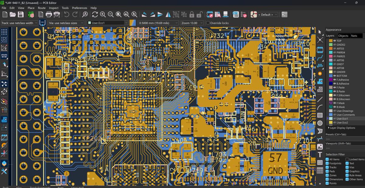
High Speed PCB Layout
#pcbdesign #pcblayout #pcbdesigner #pcb #circuitboard #pcbmanufacturer #electronicengineering #electronics #electronicengineer #pcbassembly

1
77
29 Jul 2025
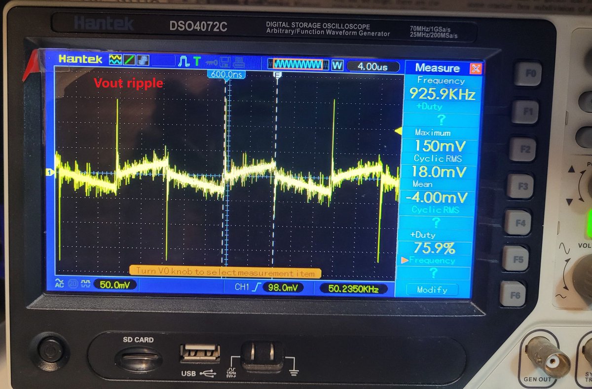
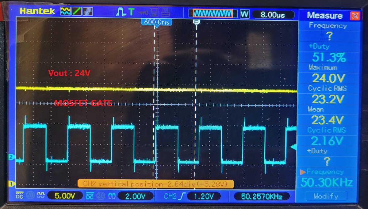
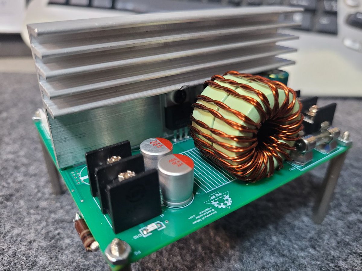
A digitally controlled boost converter designed around the STM32F405 microcontroller, capable of stepping up a 12 V input to a regulated 24 V output while delivering up to 5 A of current.
#microcontroller #12v #24v #5a #pcbdesign #pcblayout #pcbmanufacturing #pcbdesigner #electronicengineering #electronics #hardware #engineering #pcbassembly #electronicmanufacturing #technology
4
75
28 Jul 2025
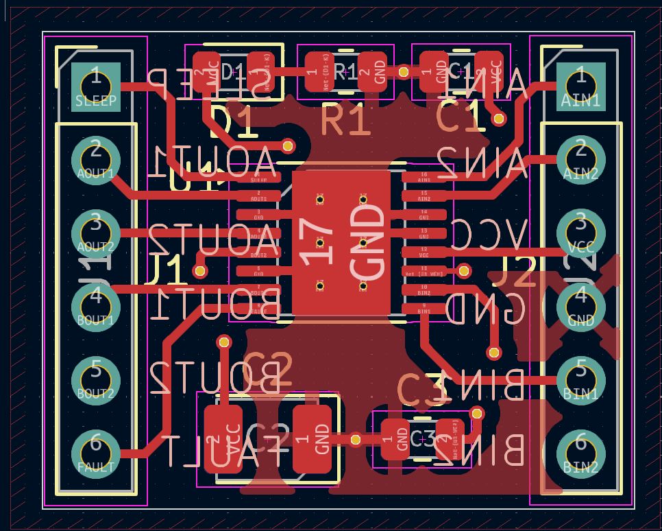
Custom DRV8833 Motor Driver Module | Designed in KiCad
#kicad #motor #pcbdesign #pcblayout #pcbmanufacturing #pcb #circuitboard #pcbdesigner #electronicmanufacturing #electronicassembly #electronicengineering


7
110
15 Jul 2025
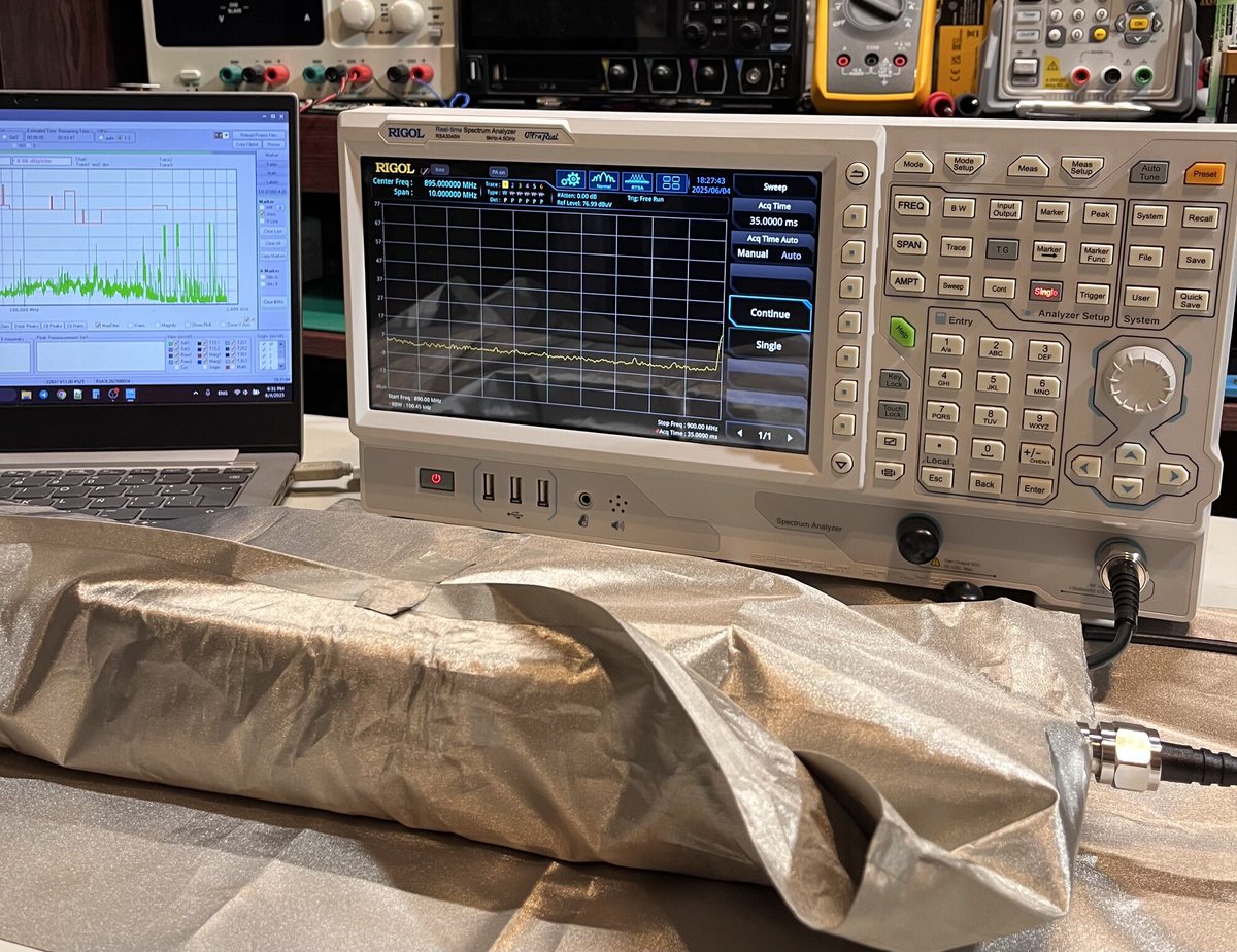
Easy Pre-Compliance CISPR Test with small TEM Cell and Real-Time Spectrum Analyzer
#pcbdesign #pcbdesigner #electronicengineering #electronicengineer #pcbassembly #pcb
4
107
12 Jul 2025
Which of the following signals is typically considered a high-speed signal ?
a. Above 1 kHz
b. Above 50 MHz to 100 MHz
c. 50 Hz AC mains signal
d. Above 1 GHz
#pcbdesign #pcbdesigner #pcb #raypcb #pcblayout #electroniceingeering #electronicengineer
1
1
5
70
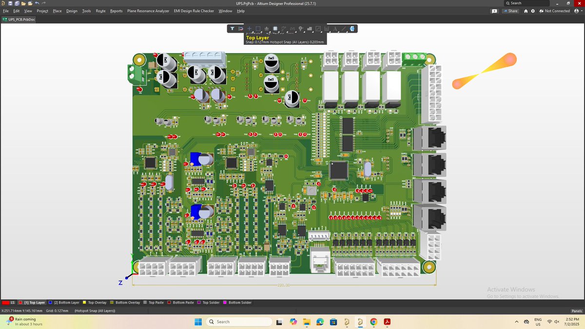
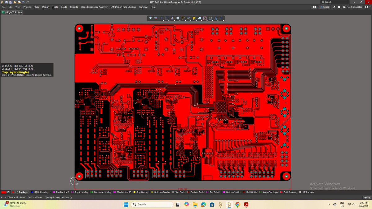
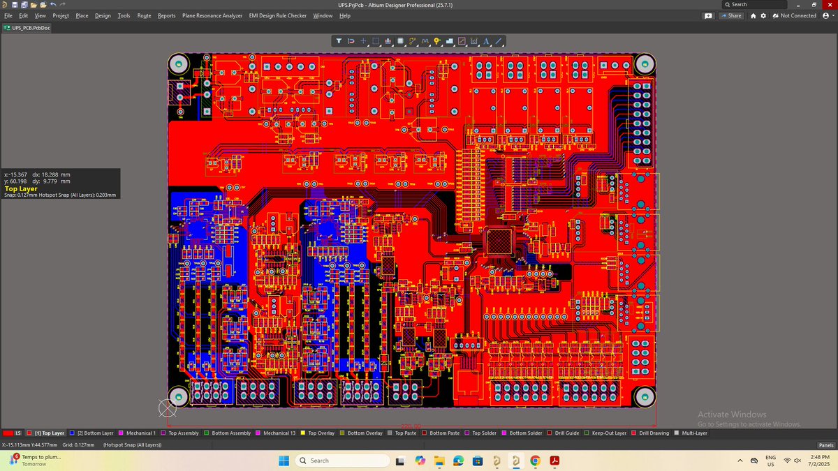
12 Jul 2025
Developed a 2-layer PCB using Altium Designer for defense-grade applications in submarine environments. This project required meeting stringent requirements for mission-critical systems where failure is not an option. The design addresses the unique challenges of underwater deployment, including extreme environmental conditions and the need for absolute reliability in power delivery systems.
The PCB features a robust 2-layer architecture specifically optimized for harsh marine conditions. Every aspect of the design prioritizes durability and performance, from thermal management to electromagnetic interference mitigation. The compact form factor delivers efficient power management for uninterruptible power supply systems while maintaining defense-grade standards throughout.
Altium Designer's comprehensive toolset enabled precise control over the entire design process, from initial schematic capture through final manufacturing preparation. The platform's advanced design rule checking and simulation capabilities were essential for validating performance under the extreme operating conditions these systems face in submarine applications.
This project demonstrates the intersection of advanced PCB design methodology and defense engineering requirements, where technical excellence directly impacts mission success and personnel safety.
#raypcb #raymingpcb #pcb #pcbdesign #pcblayout #pcbdesigner #circuitboard #pcbmanufacturer #pcbassembly #electronicmanufacturing #electronicengineering
2
71
11 Jul 2025
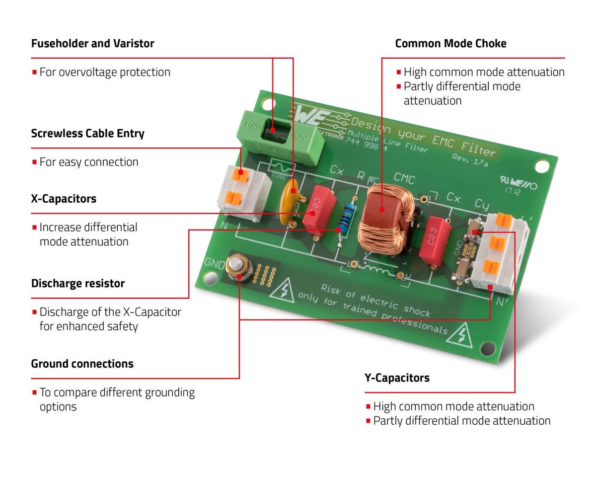
Dear your own EMC Filter
#filter #pcb #pcbdesign #pcblayout #electronicengineering #pcbassembly #electronicengineer #pcbdesigner #pcba #electronicengineering
3
136
9 Jul 2025
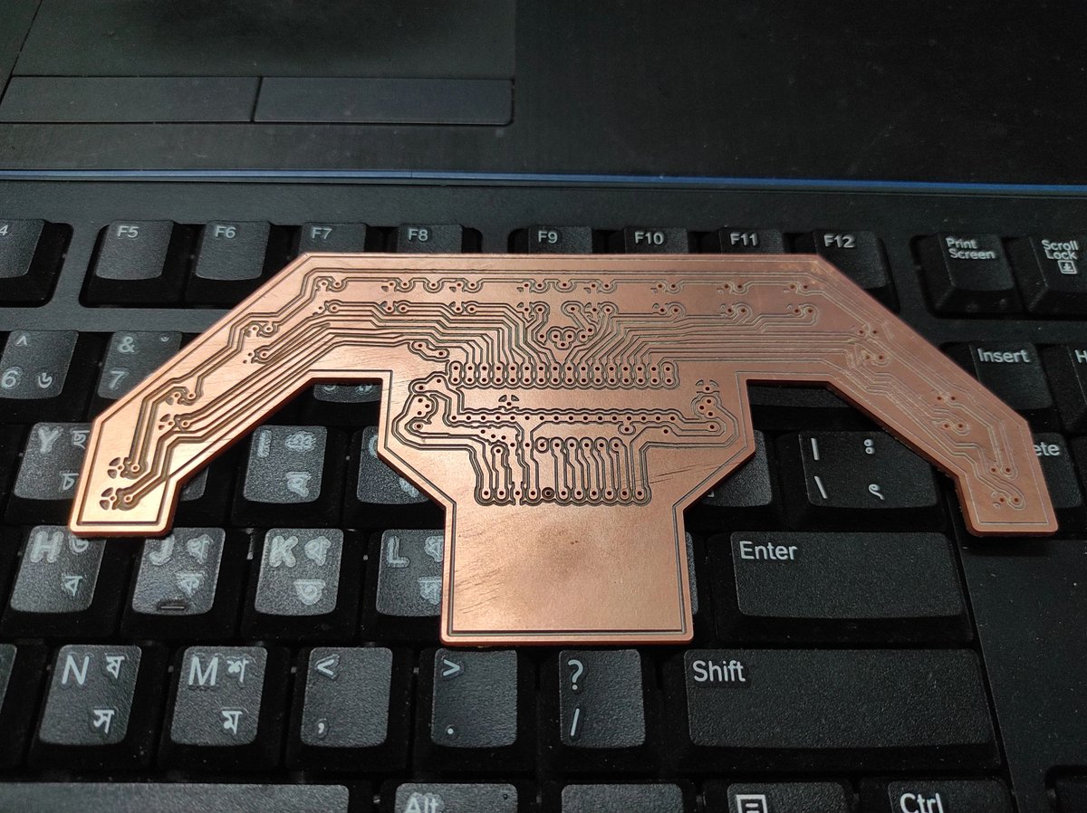
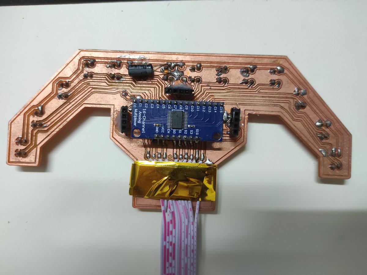
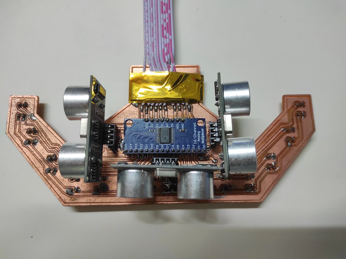
IR reflective sensor, 16 channel mux, 3 ultrasonic sonar all in a single layer PCB.
Designer: Shihabul Ehsan
#ir #sensor #ultrasionic #pcb #pcbdesign #pcbdesigner #pcblayout
#electronicengineer #electroniccengineering
1
3
69
8 Jul 2025
RF PCB Application #1
#rf #microwave #RFEngineering #MicrowaveTech #RFDesign #WirelessCommunication #MicrowaveEngineering #5GTechnology #AntennaDesign #RadarTech #RFTesting #MMWave #RFComponents #MicrowaveCircuits #SatelliteCommunication #EMIEMC #RFAmplifiers #MicrowaveFilters #radar #raypcb #WirelessNetworks #RFIDTech #PhasedArray #TelecomEngineering #pcbdesign #pcblayout #electronicengineering #pcbdesigner #pcb
1
4
74
7 Jul 2025
DIP Components - Daily Work in RAYMING Factory #6/100 #pcbdesign #raypcb #pcblayout #pcbmanufacturing #pcb #pcba #pcbdesigner #electronicmanufacturing #electronicengineering
1
5
93
5 Jul 2025
FR4 solid-state coil, planar transformer solution
#fr4 #coil #planar #transformer #pcbdesign #pcbdesigner #pcblayout #electronicmanufacturing #electronicengineering #rfengineer #military #hardware #hardwarengineer #pcbassembly #pcbmanufacturing #pcb #pcba
1
59
25 Jun 2025
Arduino project- Garbage Sorting Intelligent Control
#arduino #intelligentcontrol #diyproject #electronics #hadwre #pcb #pcbdesign #pcblayout #pcbdesigner #pcbmanufacturing
1
3
67
24 Jun 2025
What Is a 'Phased Array' in Phased Array Radar ?
#radar #arrayradar #electronicengineering #electronicengineer #pcbmanufacturing #pcbdesign #pcblayout #pcbdesigner #rf
2
6
110
21 Jun 2025
New Evaluation Board for the Texas Instruments ADS5400, The board fits new design
#pcbdesign #pcbdesigner

1
100