
Experts in Thin Film Metrology and Plasma Process Technology
Joined January 2012
- Tweets 188
- Following 138
- Followers 254
- Likes 21
18 Photos and videos


18 Apr 2023
SENTECH Instruments are part of a joint project funded by Investitionsbank Berlin as part of the ProFIT program funding. Learn about the partners and the project shorturl.at/mwFKY
1
154
SENTECH Instruments retweeted

23 Feb 2023
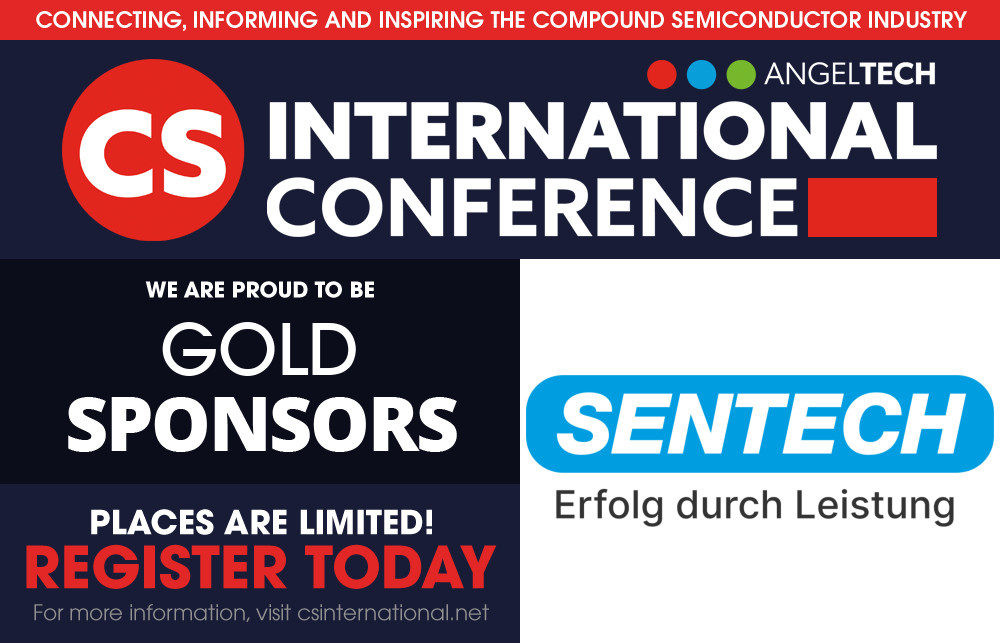
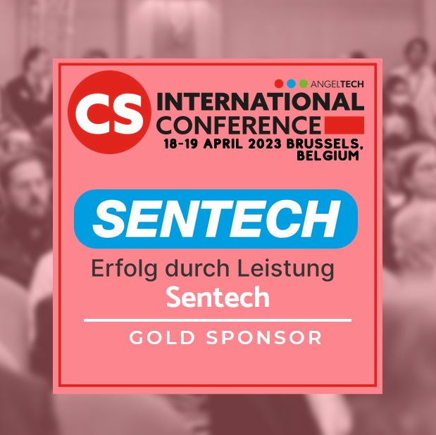
Sponsor Announcement 📢
We are delighted to announce that @SentechNews are Gold, Wifi and App Sponsor of #CSInternational! 🌟
Register for your ticket today!
Limited number tickets remaining⬇️
csinternational.net/register
1
1
170
SENTECH Instruments retweeted

Sponsor Announcement 📢
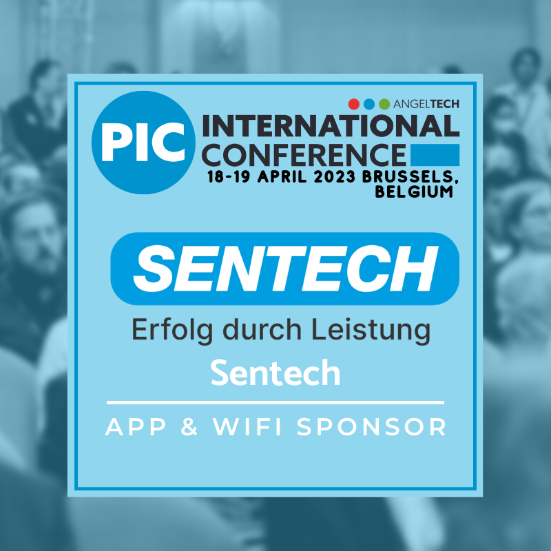
We are delighted to announce that @SentechNews are Wifi and App Sponsor of #PICInternational! 🌟
Register for your ticket today!
Limited number tickets remaining⬇️
picinternational.net/registe…
1
1
128
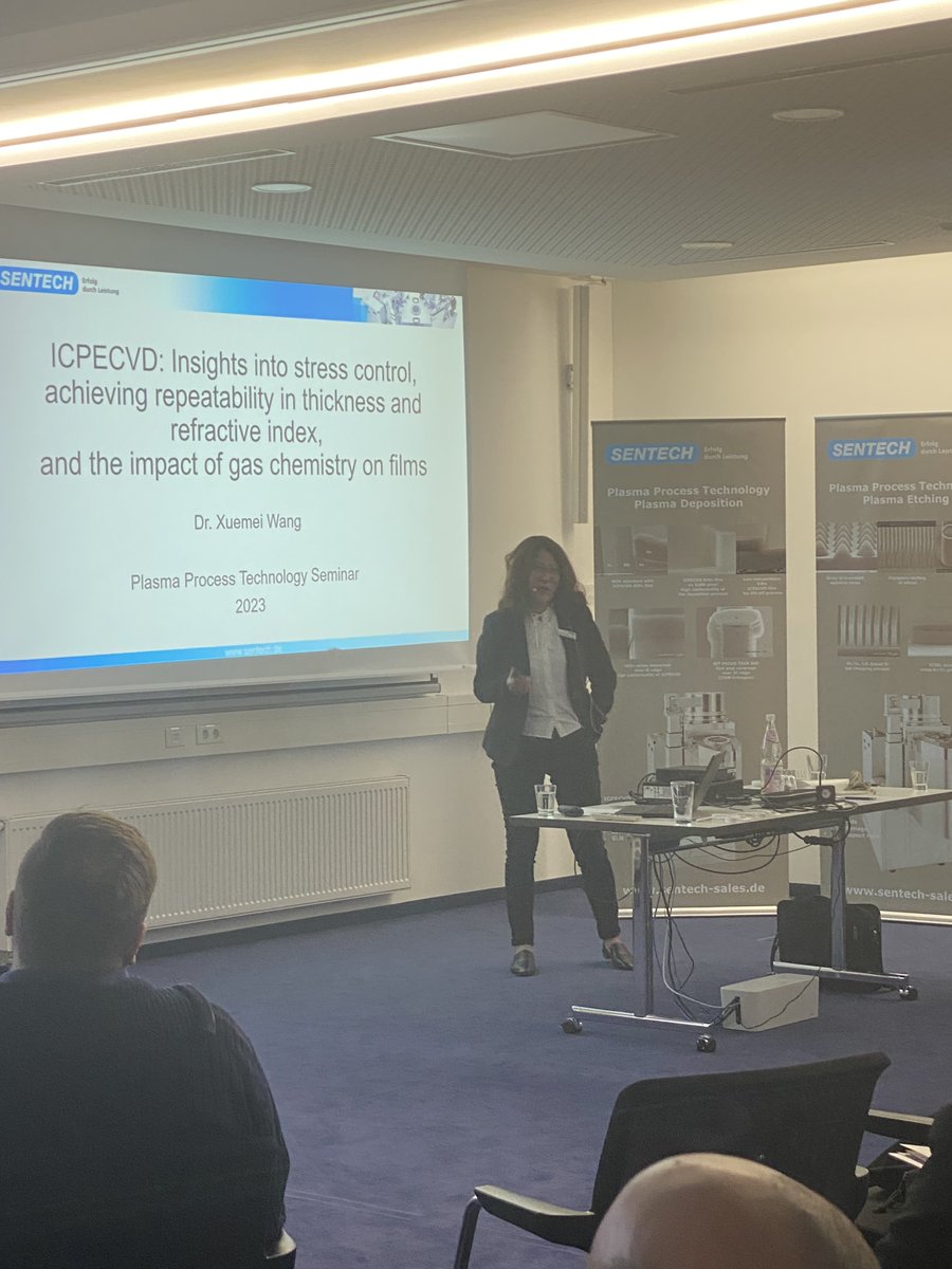
20 Mar 2023
ALD and PECVD passivation from Supracon AG, Jena, and SENTECH Instruments GmbH shared ICPECVD insights into stress control, repeatability, and the impact of gas chemistry on films, bringing the afternoon session of the #Plasma #seminar to a close.
#plasmatechnology #deposition
148
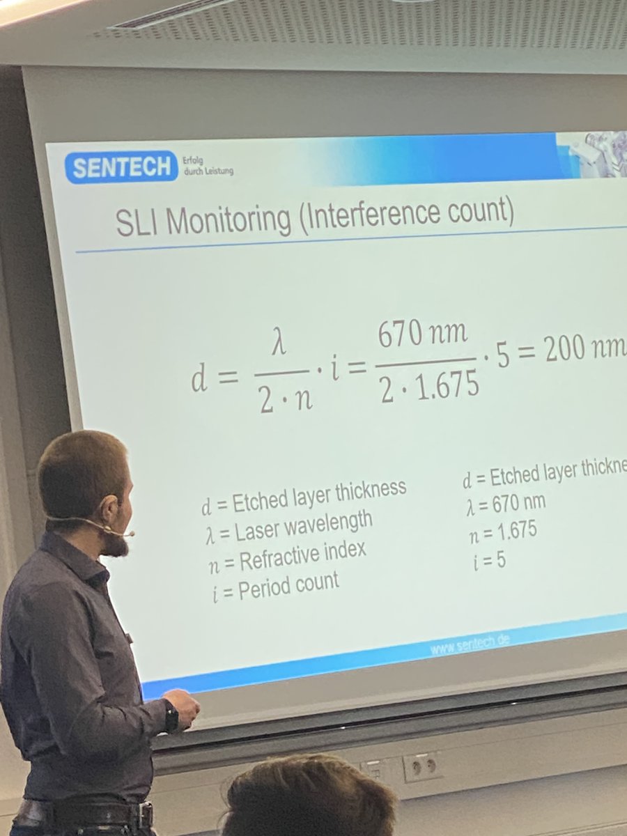
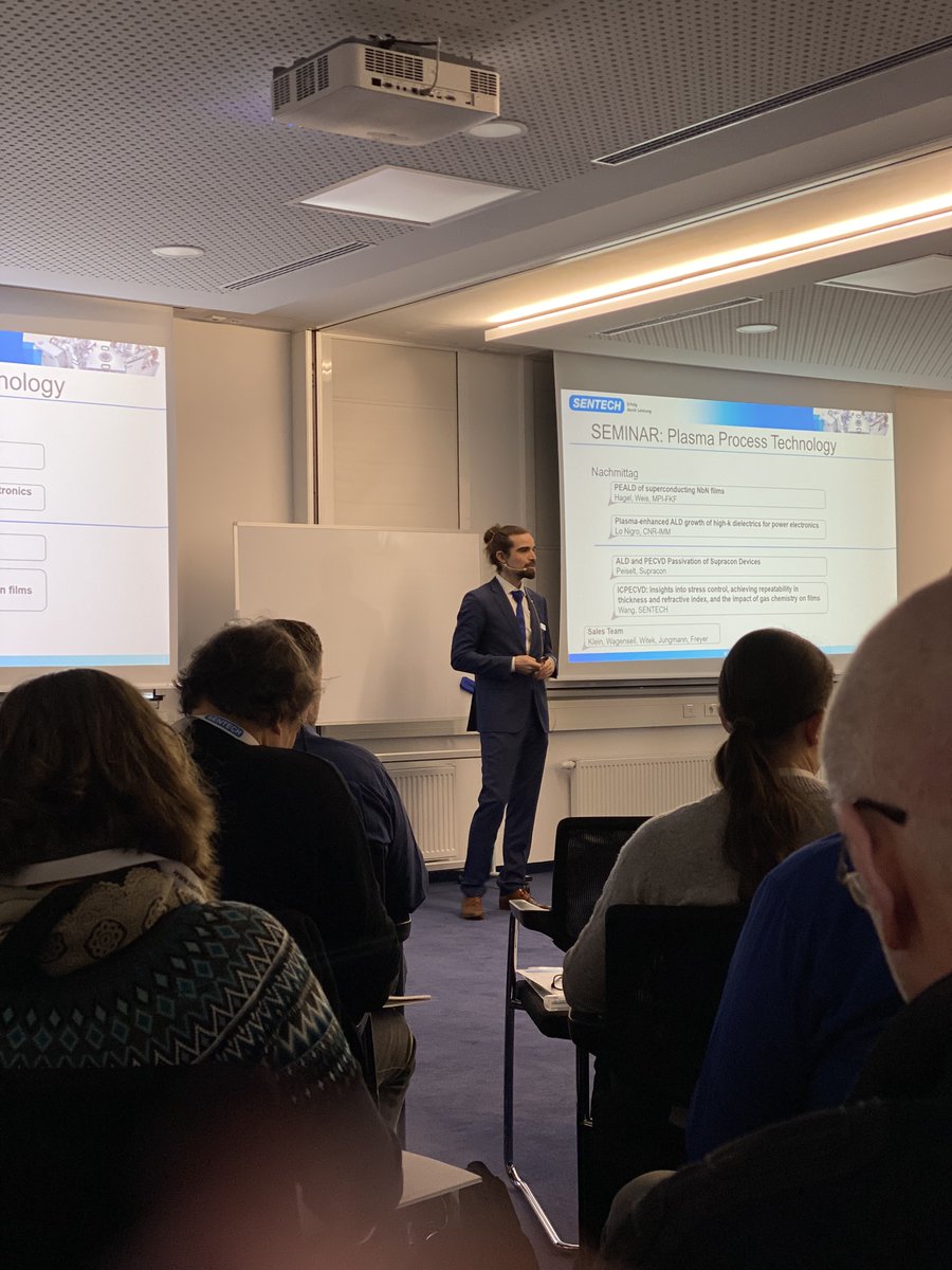
20 Mar 2023
The SENTECH Plasma Seminar #deposition topics-PEALD of superconducting NbN films from Max-Planck Institute for Solid State Research, Stuttgart, Germany, and PEALD growth of high-k dielectrics for power electronics from CNR-IMM
78
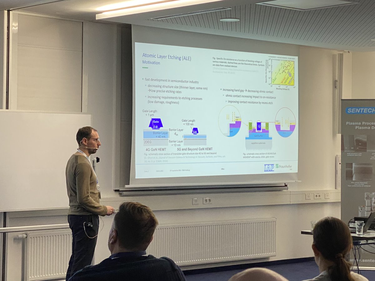
20 Mar 2023
The SENTECH Plasma Seminar with Fraunhofer IISB discussed low-damage atomic layer etching (ALE) for nitride semiconductors, and TU Chemnitz on, challenges from various applications of ICP-RIE.
#plasma #semiconductor
1
83
20 Mar 2023
The SENTECH Plasma Seminar 2023 began with an insight into AlScN and diamond etch from United Monolithic Semiconductors sharing results for different applications of the ICP etching of III/V semiconductors.
#etch #plasma #knowledge #science #semiconductors #reseaarch #industry
1
76
4 Jan 2023
SENTECH will be exhibiting and attending the 13th CS International conference. For more information about this event or to register, follow our website link bit.ly/3X2ov0j
#event #semiconductorindustry
63
15 Nov 2022
@SentechNews are at #semiconeuropa
You can visit us in Hall C1, on Strand 616
#semiconductors #exhibition #plasmatechnology #thinfilm
1
1
11 Nov 2022
SENTECH Instruments GmbH expands its sales and service offering in France. We are pleased to welcome Côme Chevailler. Read the full article bit.ly/3fUkBH9
#team #experience #france
2
8 Nov 2022
SENTECH will be exhibiting #SEMICONEuropa
(Hall C1, Stand 616). We have free day passes available, follow the link for info . bit.ly/3h8R4cU
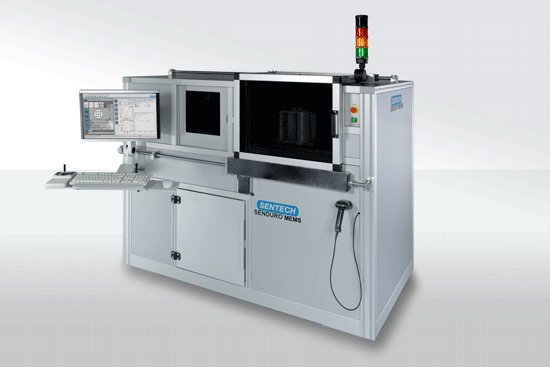
#semiconductorindustry #plasmatechnology #metrology #2dmaterials #powerelectronics #optics #sensors #led #lasers #mems
1
26 Oct 2022
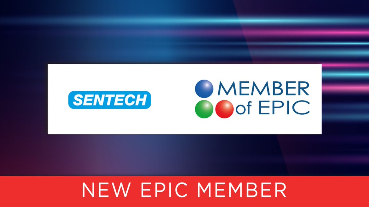
As experts in the areas of #plasmaprocesstechnology and #thinfilmmetrology, SENTECH are a proud member of @EPICassoc . We look forward to working with the team at EPIC and our fellow members to continue driving the sustainable advancement of the European photonics industry.
1
2
SENTECH Instruments retweeted

24 Oct 2022
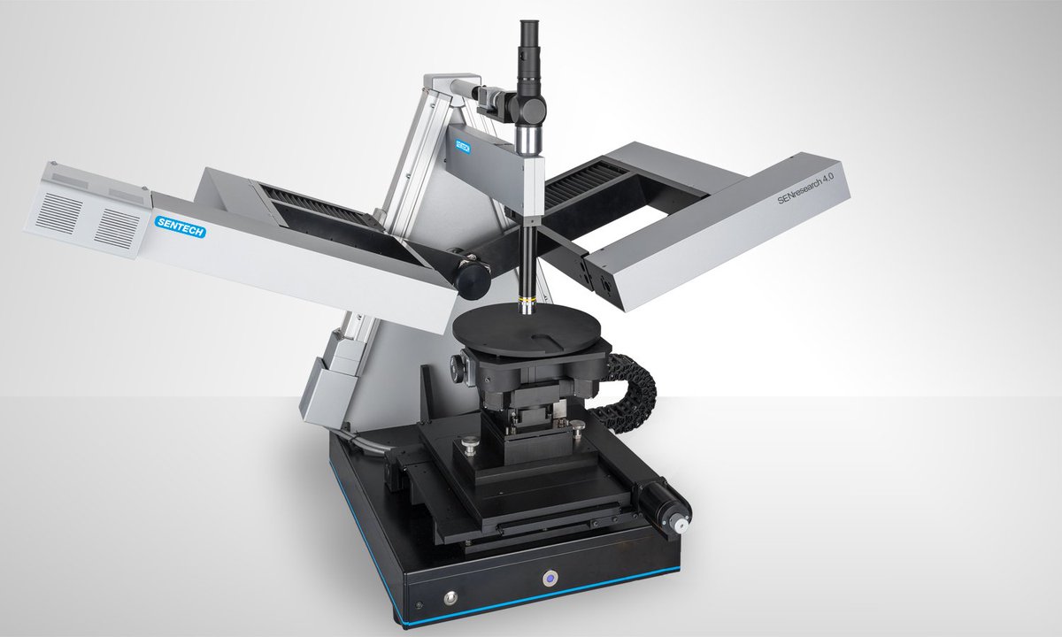
Join us in welcoming new EPIC member, @SentechNews, who develops, manufactures and sells advanced-quality instrumentation for Plasma Etching, PECVD, Atomic Layer Deposition, Thin Film Measurement, and Photovoltaics.
sentech.com
#EPICmembers #photonics #photovoltaic
1
2
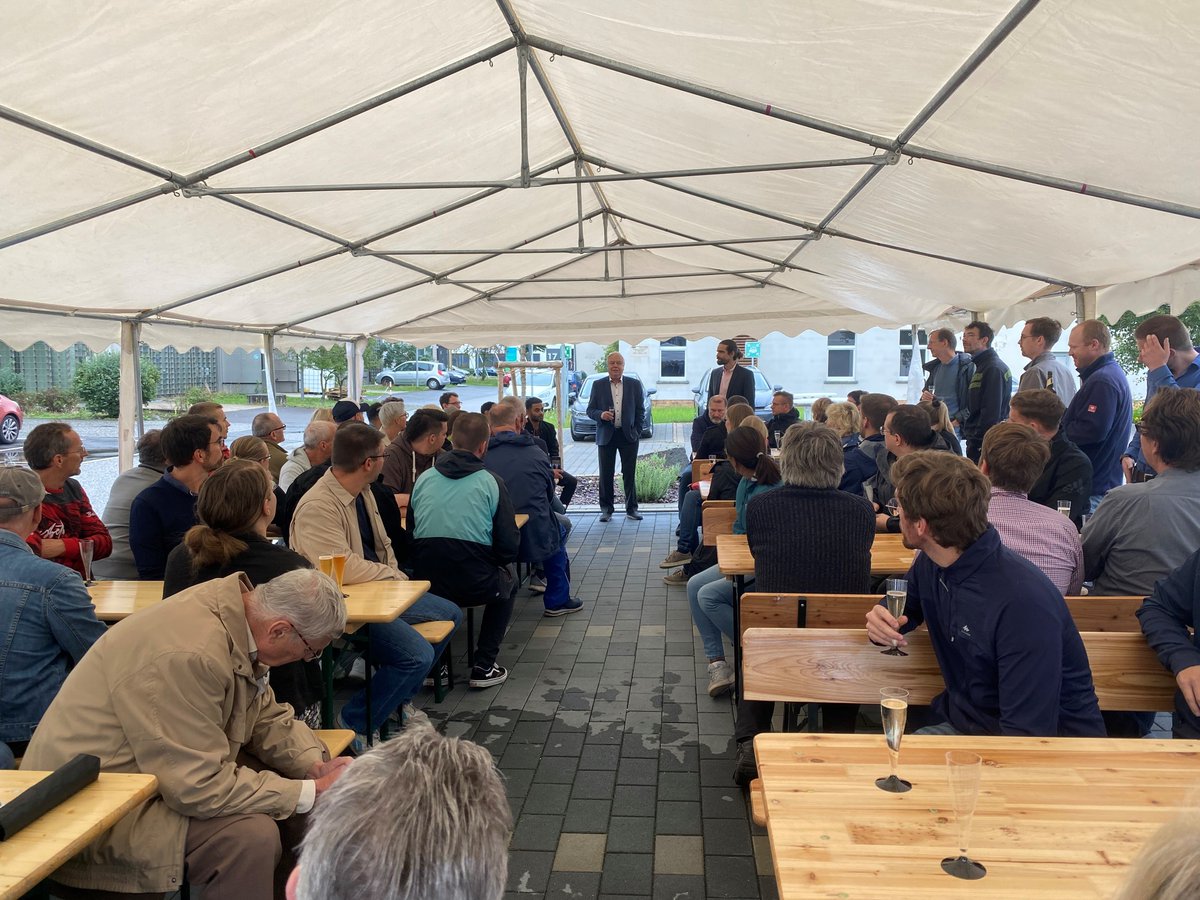
14 Sep 2022
The SENTECH Instruments team in Berlin came together yesterday to celebrate 32 years as a leading supplier of plasma process technology equipment spectroscopic ellipsometry instruments. #technology #business #team #success #scienceandtechnology #growth #work
1
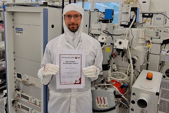
12 Sep 2022
During the GaN Marathon 2022, promising results for gallium nitride in microelectronics and optoelectronics were presented by Christian Miersch, PhD student at Fraunhofer IISB, who received a “Best Student Presentation Award” .
bit.ly/3eAL8YN.
#research #phd #award
1
1
2 Sep 2022
SENTECH are collaborators on this innovative and exciting research with the picT2DES #ForLab team #Mikroelektronik Bochum for 2-Electronics at the Ruhr University Bochum. Learn more about this novel, resource-saving electronic system. rb.gy/r4iy3j
SENTECH Instruments retweeted

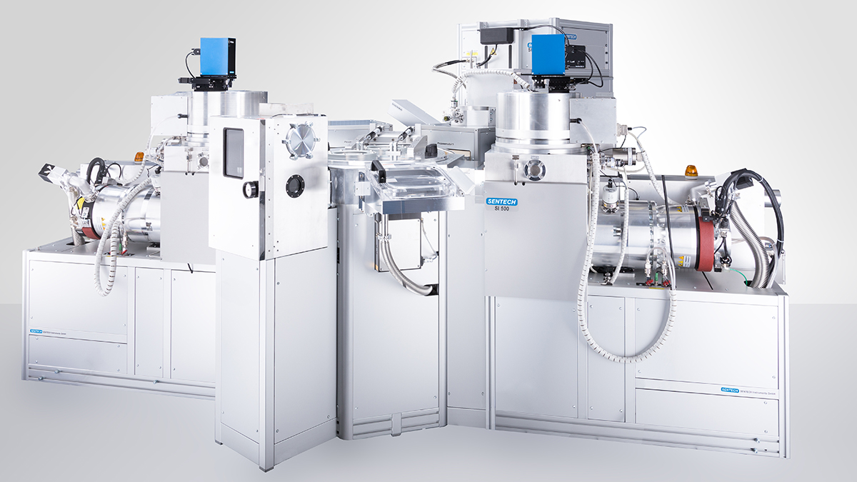
⚙️ #machinecloseup : For the development of novel device concepts like lateral metal-insulator semiconductor field-effect transistor #MISFETs and vertical #GaN-transistors, #FMD institute @FBH_News has put a new 4-chamber cluster tool manufactured by #SENTECH into operation 👇

Novel ALD-etch cluster #tool opens up new possibilities for highly integrated #device concepts. It allows to #etch, #anneal & deposit in one single tool, thus offering well-defined surface conditions & a low level of cross-contamination.👉fbhlink.de/tgsq
#semiconductor
1
4

Novel ALD-etch cluster #tool opens up new possibilities for highly integrated #device concepts. It allows to #etch, #anneal & deposit in one single tool, thus offering well-defined surface conditions & a low level of cross-contamination.👉fbhlink.de/tgsq
#semiconductor
2
2