
A real 6-layer high-frequency hybrid PCB build.
Material: RO4835 RO4350
Min. hole size: 0.25 mm
Hole density: about 113,900 holes / ㎡
#HighFrequencyPCB #HighSpeedPCB #RFPCB #RogersPCB #PCBManufacturing #MicrowavePCB #PCBPrototype #ElectronicsManufacturing #MCHDIPCB

2

Engineer:
“Signal integrity is complicated.”
Back-drilled PCB:
“Not after removing the giant copper antenna inside your via.”
#JLCPCB #HighSpeedPCB #Electronics #HardwareEngineering

3
20
11,105
High-speed PCB Stackup: 4 Layers vs 6 Layers
4 layers: Lower cost, simpler, limited routing/signal integrity. 6 layers: Better for high-speed signals, more routing, lower EMI (ideal for dense boards). Designed dense high-speed PCBs? Share your tips!
#HighSpeedPCB #6LayerPCB
2
6
1,042

Jan 21
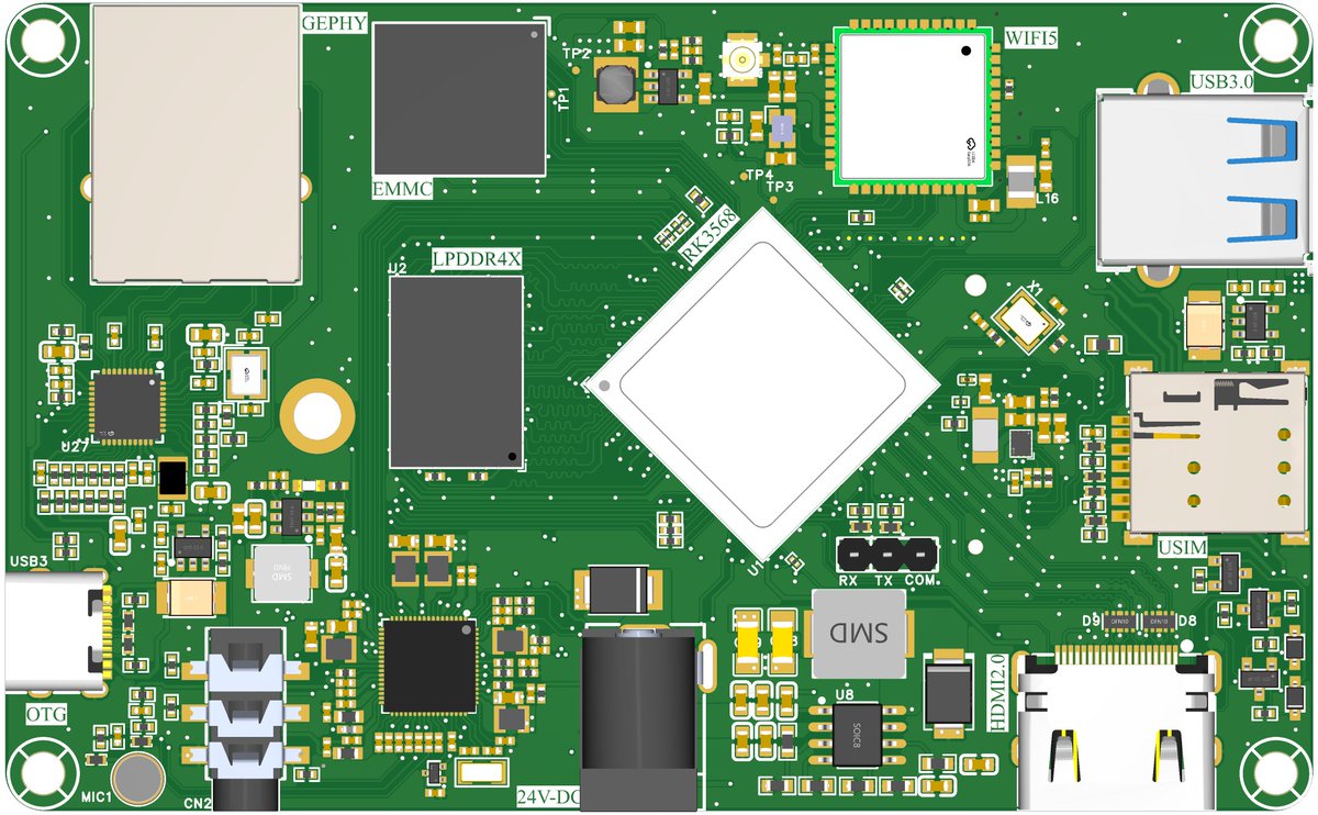
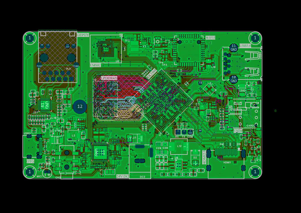
☘️RK3568 SBC Design with Quectel 5G Module
6-layer PCB layout, RK3568, LPDDR4X, Ethernet, USB3.0, USB2.0, Audio Codex, HDMI, SD Card, WiFi & BLE Module, and M2 Slot, Customized Android OS
#Rockchip #RK3568 #ARM #EasyEDA #HighspeedPCB #multiplelayers #Prototyping #sbc

1
62

30 Dec 2025
EMI issues aren’t random — they’re PCB layout mistakes.
9 essential EMI rules for high-speed PCB design: routing, return paths, impedance & more.
How many do you follow? 👀
#PCBDesign #EMI #HighSpeedPCB
1
1
179

17 Jul 2024
Trouble in Your Tank: Materials for PWB Fabrication—Drillability and Metallization. @IPCassociation consultant Mike Carano considers requirements for high-speed data transmission and the level of importance materials play. #highspeedpcb #signalintegrity bit.ly/3Sa3Pn2
1
2
74

3 Aug 2022
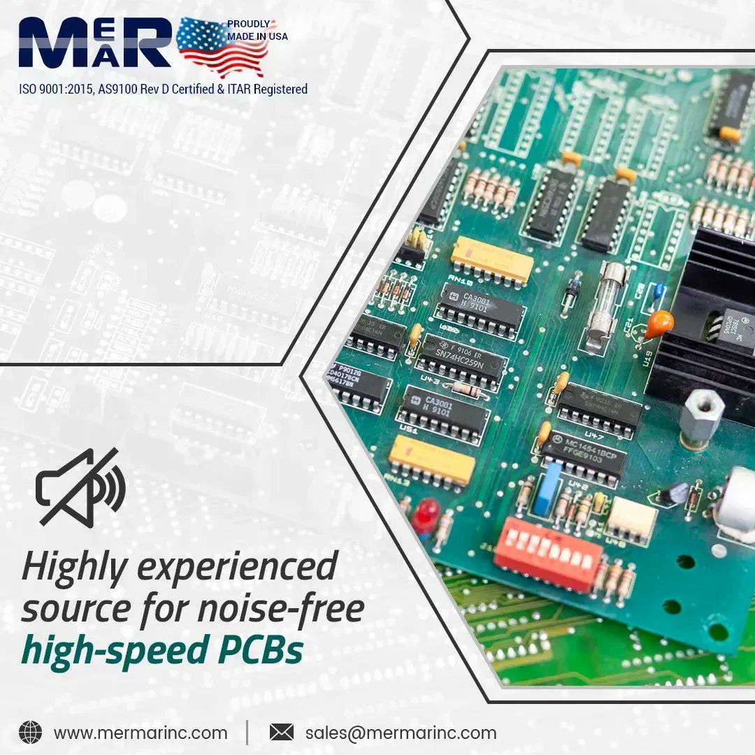
Our specialty is offering a noise-free, high-speed PCB manufacturing solution to satisfy the PCB needs of various industry verticals.
buff.ly/2ZeLFZq
#PCBs #HighSpeedPCB #PCBManufacturing #PrintedCircuitBoard #PCBManufacturer #USA #California
1
20 Jun 2022
Right from the schematic to the final Gerber files, we have robust experience in designing #HighSpeedPCBs. Send us an inquiry now!
buff.ly/3Qxzi0g
#PCB #PCBs #PCBA #HighSpeedPCB #PCBDesign #PCBManufacturing #HighSpeedPCBDesign #USA #California
3

16 Feb 2022
Designing Practices for Successful High-Speed PCB Assembly:bit.ly/36kNkjd
#HighSpeedPCB #PCBassembly
2

30 Sep 2020
Join us in supporting #IMAPS2020. Steven Watt presents how to choose the best SiP implementation options during the on-demand technical sessions available from 10/6-10/30. #speakingopportunity #gettoknowzuken #systeminpackage #highspeedpcb
okt.to/0nfi36

1

7 Aug 2020
If You Don't Know, Now You Know.
What is the purpose of nickel plating on PCB?
✅Learn more: bit.ly/31wFI7f
.
.
#MultiLayer #AdvancedPCB #HighSpeedPCB #PCBWay #PCB #MicroVia #BuriedVia #BlindVias #ENIG #ENEPIG #SurfaceFinish #nickel

2
17 Jul 2020
If You Don't Know, Now You Know.
The Formation and Prevention of Black Pad and Phosphorus-Rich Layers.
👉Learn more: bit.ly/32uCFyi
.
.
#MultiLayer #AdvancedPCB #HighSpeedPCB #PCBWay #PCB #MicroVia #BuriedVia #BlindVias #ENIG

3
10
25 Jun 2020
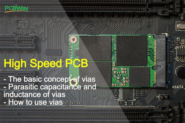
If You Don't Know, Now You Know.
- How to avoid the negative effects of vias in high-speed PCB design?
✅Learn from PCBWay: bit.ly/3hUDqWR
.
.
#MultiLayer #AdvancedPCB #HighSpeedPCB #PCBWay #PCB #MicroVia #BuriedVia #BlindVias
1
9