
Joined February 2018
- Tweets 4,703
- Following 948
- Followers 85,214
- Likes 281,074
82 Photos and videos


Pinned Tweet

23h
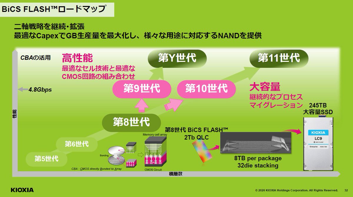
革ジャンが次の1兆ドル企業と名指ししたMarvellについてnoteを書きました。
ハードディスクから生まれ変わり、XPU Attach市場をどのように開拓するのか?
詳しく解説しています。
是非、読んでみてください。
note.com/paul1211/n/nd13fdfe…
9
19
239
97,152


51m
😎

9
7
10,537
1h
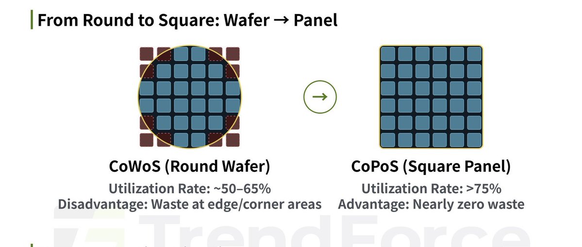
In terms of physical productivity, the square panel (CoPoS) is highly efficient as it leaves virtually no waste. However, the inability to utilize the existing 300mm wafer ecosystem, particularly for wafer-level testing, is expected to be a major challenge. Many companies will likely struggle with defect isolation and removal at the CoP (Chip on Panel) stage.
7
2
20
10,995
2h
既にAIの勃興が起きてしまった異常事態の中で過去の平均に回帰する、外れた異常値は元に戻るという前提がおかしいと思うんですよね
固定の箱の中の事象を観察している訳ではないのに、何かを異常値としてラベル付けすることがナンセンスだと思っています
最善は過去のバイアスを捨て現状を正しく認識することかなと

バブルであるか否か、
近く弾けるか否か
時間軸と規模含め、
現時点では「わからん」 ってのが
バイアスのない真っさらな目でみた感想だと思うんですが。
今どちらかに決めつけるのであればそれはバイアス入ってると思いますね。
16
5
87
22,024
3h
ありがとうございます
そう言って頂けると励みになります
質問などコメント欄にてどんどん書いてくださいっ

MRVLは気になってたので購読。
いつもながら内容素晴らしいです👏
9
1
24
16,134
3h
Yes, Glass carrier is just a carrier. Actually real CoPoS product should not have glass just under RDL.

Glass carrier should move out….🤣 and why are solder balls under glass carrier?
9
21
20,702
パウロ retweeted

4h
お褒めいただきありがとうございます🙌 利益成長、そしてマーケットの許容PER、そしてAI半導体が全て…🥹

ゆきママのすごいところは一貫してるところです
2020年のコロナショックの時から見てますが、目線がブレないのがリスペクト
10
6
103
32,757
4h
的確な考察ありがとうございますっ

この投稿の「関東電化・セントラル硝子が7月から恒久的に生産停止の見込み」、一次情報では裏付けが取れません。
①出所:この“恒久停止”はThe Elec原報になく、中国商品系メディア(ChemNet/财联社系)の二次報道。The Elec原文は「下半期の供給は不透明」までで、“7月恒久停止”の文言はなし。続く
4
1
31
28,600
4h
そうなんです。しかも中国でも大きな需要がある。

4
4
98
38,106
4h
RT @Biz_zatukora: いつのまにかアップル・マイクロソフトというアメリカ産業の頂点をAIの頂点Nvidiaが抜き去って行ったのと同じなんでしょうね。
そしてサムスン・SK・MUが揃って1兆ドルへ踏み入れたこの流れを見れば、
日本企業でそれに当たるキオクシアがAI代…
16
4h
昨日投稿しましたMarvellのnote大好評です
完全に生まれ変わった彼らの製品ポートフォリオを解説しています
是非、読んでみてください
note.com/paul1211/n/nd13fdfe…
5
2
48
21,872
4h
今年後半もCPUとメモリですかね
AI需要の高まりがCPU不足を引き起こす!サーバーの供給は需要を下回るものの、半導体市場の見通しは下半期も堅調だ。
工知能(AI)への需要は依然として高く、新華社、UMC、VISをはじめとする多くの国内半導体メーカーは、下半期の業界業績が上半期よりも改善すると楽観視している。半導体シリコンウェハーメーカーの泰盛科技も、下半期の見通しについて楽観的な見方を示している。
業界関係者の多くは、AIに対する旺盛な需要が、今年後半の業界繁栄の主要因であると考えている。特に、AI搭載デバイスの普及に伴い、従来型サーバーの需要が予想以上に高まり、中央処理装置(CPU)の需要が急増し、市場は供給不足の状態にある。
サーバー管理チップメーカーのASUSTechは、顧客需要は堅調だが、業績に影響を与える最大の要因は供給側だと指摘した。ASUSTechはパッケージングサプライヤーを追加しており、今年の業績は四半期ごとに成長すると見込んでいる。下半期の業績は上半期を上回り、第3四半期の業績は第2四半期を上回り、第4四半期の業績は第3四半期を上回る見込みだ。
ウェハー製造会社であるUMCは、電力管理チップ市場の旺盛な需要を主な要因として、今年後半に事業が徐々に回復すると見込んでいる。同社は、22nmプロセスが総売上高に占める割合が大きくなり、これが成長の主な原動力になると予想している。
半導体シリコンウェハーメーカーの泰盛科技(Taisheng Technology)の観察によると、顧客の在庫戦略は在庫削減から在庫補充へとシフトしている。半導体シリコンウェハー業界は底を脱し、受注見通しは大幅に改善しており、下半期の事業見通しは明るい。
RFチップメーカーのRichwaveは、メモリなどの原材料価格の高騰がネットワーク市場における受注見通しに影響を与えていると述べた。しかし、新規プロジェクトの継続的な進展により、下半期の売上高は上半期よりも改善すると見込んでいる。
高速伝送インターフェースチップメーカーのASMediaは、下半期の業績見通しについて比較的慎重な姿勢を示している。ASMediaは、メモリ価格の高騰とCPUの供給不足によりマザーボード顧客からの需要が減少しており、この傾向は下半期も続く可能性があると指摘。これによりASMediaの業績に影響が出ると見込んでおり、自社製品事業の拡大を加速させる方針だ。
11
7
141
20,719
4h
半導体インフレへ
やはりAIがすべてを食べて、インフレ率を引き上げる
ウェハー製造工場におけるコスト上昇は、さらなる価格上昇につながり、半導体インフレのサイクルを長期化させる可能性がある。
コスト上昇に直面し、ウェハー製造会社は製造価格の引き上げを継続する可能性があり、IC設計会社もそれに追随して価格を引き上げるだろう。半導体価格の高騰はさらに深刻化し、携帯電話をはじめとする端末市場に不確実性をもたらす可能性がある。
水、電気、原材料価格の高騰、労働力と生産能力への需要増加、そして地政学的要因による多様な地域での生産能力需要の高まりにより、ウェハー製造工場はコスト圧力の増大に直面している。
コスト上昇の影響を緩和するため、ファウンドリのパワーチップ・テクノロジーとVISは今年、相次いでファウンドリ価格を引き上げた。UMCも今年下半期に一部価格を引き上げる予定であり、来年には顧客と価格調整についてより包括的な協議を行うと発表した。
VISは将来的な価格調整の可能性を否定していません。VISは、コストの上昇や投資の継続が続く場合、市場の変化、競争環境、顧客ニーズを注視し、顧客と価格調整の範囲について検討すると述べています。
年次株主総会で、TSMCの会長兼社長である魏C.C.氏は、株主からの価格引き上げに関する質問に対し、「価格を引き上げたいと考えており、現在その取り組みを進めている」と回答した。さらに、TSMCの粗利益率は40%超から50%超に上昇し、現在は60%を超えているとし、これはTSMC従業員の努力の賜物だと述べた。そして、ウェハー価格はTSMCが本来持つべき価値を反映すべきだが、メモリメーカーとは異なり、価格が突然4倍になることはないと強調した。
IC設計会社のMediaTekは、AIコンピューティング能力に対する需要の急速な増加が、グローバルサプライチェーンにおける技術革新と構造変化を促していると述べた。業界チェーンにおける価格上昇は、今後常態化すると見込まれる。MediaTekは今後もサプライチェーンとの連携を継続するとともに、高騰するサプライチェーンコストを適切に転嫁できるよう価格調整も検討していく。
ウェハー製造サービスの価格上昇に加え、後工程のパッケージングおよびテスト会社も価格を引き上げている。センシングチップメーカーのPixArt ImagingとパネルドライバICメーカーのAtomiumは、粗利益率の安定を確保するため、価格上昇の可能性について情報を発表した。
半導体チップなどの部品価格の高騰は、携帯電話をはじめとする端末製品市場に不確実性をもたらしている。携帯電話メーカー各社は、ハイエンド製品市場に注力する一方で、製品価格の調整を行うなど、製品市場戦略の見直しを進めている。しかし、これは消費者の購買意欲に影響を与え、結果として売上減少につながる可能性がある。
6
5
107
22,348
5h
そんなことがあるんか!
7月24日に10%の暫定関税が失効し、ハイテク製品の出荷が急増したことを受け、北米の航空貨物運賃は10%上昇した。
米国が輸入商品に課していた10%の暫定関税が7月24日に期限切れとなるため、世界のサプライチェーン全体で早期出荷が急増している。最新の市場価格によると、台湾から北米への航空貨物運賃は再び約10%上昇し、1キログラムあたり約330台湾ドルに達し、今年最高値を更新した。これは、航空貨物市場が予定より早くピークシーズンに突入したことを示している。
業界関係者は、航空貨物運賃の値上げの背景には主に2つの要因があると指摘している。1つ目は、米国の関税政策が世界中の貨物所有者による出荷ラッシュを引き起こしたこと、2つ目は、AIサーバーや半導体製造装置といったハイテク製品の大規模輸送が需要を押し上げ、貨物スペースの供給を増加させたことである。
コンテナ輸送価格も回復しており、台湾や中国本土から東南アジアへの海上・航空貨物輸送は「出荷ラッシュ」モードに入っている。最新のコンテナ輸送運賃は、極東から米国西海岸への輸送で前週比12.1%、米国東海岸からの輸送で10.1%上昇している。
航空物流業界のアナリストによると、パンデミック以前は、台湾から米国西海岸への航空貨物運賃が1キログラムあたり100台湾ドルを超えることは、非常に魅力的だと考えられていた。市場は2025年に上昇に転じ、平均価格は200台湾ドル以上を維持した。2026年に入っても、閑散期でも価格は200台湾ドルで安定していたが、旧正月の輸送需要の急増により、米国西海岸ルートでは220台湾ドル、米国東海岸ルートでは約240台湾ドルまで価格が上昇した。
真の転換点は5月に訪れた。米国の関税期限が近づくにつれ、世界の貨物輸送業者は出荷を加速させ、航空貨物運賃は6月に300ドル台に迫った。現在、北米路線の運賃は1キログラムあたり約330ドルに達しており、以前と比べて約10%上昇していることから、市場の強い需要がうかがえる。
商品の輸送ラッシュに加え、AI産業もこの需要急増の大きな原動力となっている。近年、世界のテクノロジー大手はAIへの投資を拡大し続けており、サーバー、半導体製造装置、ハイエンド部品の需要が急増している。台湾は世界のAIサーバーサプライチェーンにおいて重要な位置を占めており、主要な輸送拠点となっている。
AIを活用した貨物輸送手段が次々と登場する中、チャイナエアライン(2610)とエバー航空(2618)は貨物事業で大きな恩恵を受けている。両社は中国国内最大の貨物機保有数を誇り、貨物に対する持続的な高需要は収益成長の重要な原動力となっている。
航空物流大手CLSA (5609)は、世界のサプライチェーンが現在、海上輸送から航空輸送への異例のシフトを経験していると指摘する。不安定な原材料供給、AI業界における資材争奪戦、納期プレッシャーの影響を受け、多くの高付加価値商品が航空輸送への切り替えを選択している。輸送能力の逼迫と割増料金の増加が相まって、運賃の上昇が市場トレンドとなっている。
7
4
44
14,169