
Mapping macro trends into value chains, bottlenecks, and tickers
Joined June 2025
- Tweets 460
- Following 17
- Followers 216
- Likes 73
84 Photos and videos


Pinned Tweet

I turn messy industries into a clean structure.
Every week:
• the mega catalyst shaping an industry
• the value chain: who gets paid, who gets squeezed
• the bottleneck: where pricing power concentrates
• the tickers and catalysts: the practical takeaway
Research you can actually use.
Full research: link in bio
5
1,261
$MRVL and $AVGO just committed to a combined ~$35B in custom silicon by FY2029.
Nobody has modeled the packaging.
Every custom AI chip requires $TSM CoWoS.
Current throughput covers roughly one-third of what these two vendors alone have committed.
Marvell: ~$1B in annual TSMC prepayments.
Broadcom proportionally: ~$3B. That $4B/year is the hidden funding for a CoWoS build that hasn't been announced.
Either TSMC announces the largest packaging expansion in semiconductor history,
$INTC Foundry wins overflow, or a major program slips.
One of those three happens by 2028.
1
374
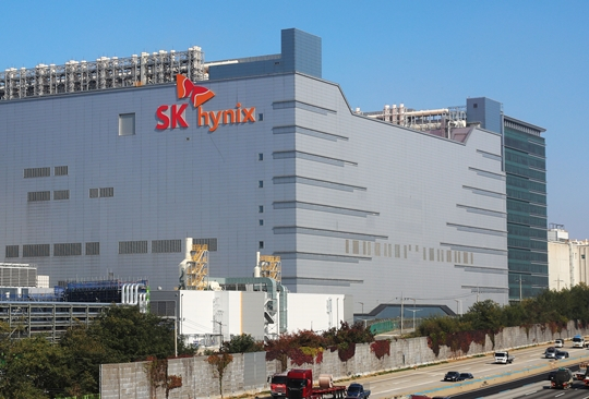
$BESI is simultaneously in evaluation at Samsung, SK Hynix, and a third memory maker, likely $MU.
That's the entire HBM supply chain.
One cycle.
If all three qualify in Q2 2026: sole-source across 100% of HBM production.
No other equipment company has a binary event this large sitting on a single decision window.

Netherlands' BESI: Samsung's Hybrid Bonding Adoption Decision Coming Soon
Samsung Electronics is expected to introduce hybrid bonding technology — projected to be at the heart of next-generation semiconductor production — around the middle of this year.
Dutch back-end equipment company BE Semiconductor Industries (BESI) stated during its Q1 earnings conference call on April 23 that "we should see more definitive news around the middle of this year regarding Samsung Electronics' (hybrid bonder adoption)." This is largely consistent with the outlook shared during the Q4/full-year 2025 earnings call in February, which indicated Samsung would adopt hybrid bonding in Q2.
Unlike conventional thermo-compression (TC) bonding, hybrid bonding does not use fine metal bumps to connect stacked semiconductor dies. Instead, it is an advanced packaging technology that directly connects the copper (Cu) surfaces of two chips. When applied to High Bandwidth Memory (HBM) and new high-layer-count NAND flash, it can deliver performance improvements, reduced power consumption, and cost savings — because the direct copper-to-copper connection enables higher integration density and shorter interconnect lengths.
That said, some observers suggest that hybrid bonding adoption could be delayed as the Joint Electron Device Engineering Council (JEDEC) moves to relax packaging height limits for next-generation HBM. On this point, BESI CEO Richard Blickman explained, "The only reason (JEDEC) is looking to relax HBM thickness specifications is because one of the three memory companies needs that height for its process," adding that "the other two are not affected by this change." The major HBM players are Samsung Electronics, SK Hynix, and Micron. The implication is that two of these three are pursuing hybrid bonding adoption for reasons beyond height considerations.
Hybrid bonding produces chip-to-chip gaps of around 7 micrometers (㎛), which makes it advantageous for reducing the total thickness (height) of HBM packages. JEDEC is reportedly considering raising the height limit from the current 775㎛ to either 825㎛ or 900㎛. Analysts argue that if the package height limit is relaxed, the lifespan of existing TC bonding technology would be extended, while the introduction of hybrid bonding could be delayed — since hybrid bonding would no longer be required simply to reduce thickness.
Blickman emphasized, "The advantages of hybrid bonding over conventional TC bonding — faster circuit speeds, lower power consumption, and reduced heat — are being increasingly clearly demonstrated," and "as Samsung Electronics has publicly disclosed, because of these technical benefits, (the relaxation of HBM thickness limits) has not changed the pace or rate of hybrid bonding adoption."
Samsung Electronics introduced its hybrid bonding technology for HBM at NVIDIA's annual developer conference, GTC 2026, last March. At the time, Samsung stated that hybrid bonding improves thermal resistance by more than 20% versus TC bonding and supports 16-high and higher stacks. Interconnect density is also higher. According to BESI, hybrid copper bonding (HCB) offers 15× the interconnect density of TC bonding and more than 100× the energy-efficiency performance (EEP).
BESI expects mass production of hybrid-bonding-based HBM to begin next year. Blickman explained, "All three manufacturers are conducting equipment evaluations against the same criteria set by a specific end customer," and "that end customer has asked the memory makers to secure hybrid-bonded stacked products by the end of this year, with the goal of bringing finished products to market next year." The end customer in question is most likely NVIDIA.
BESI is regarded as the global leader in the hybrid bonding equipment market. It holds a technological edge in both precision and throughput, particularly in die bonding equipment. Applied Materials, the world's largest semiconductor equipment company, holds a 9% stake, making it BESI's largest shareholder.
1
2
346
Every analyst is modeling agentic AI as a GPU story.
It's also a storage story, and a much less crowded one.
Agentic AI doesn't make one model call. It makes dozens, writing state to storage between each one.
That's a demand that doesn't exist in single-shot inference.
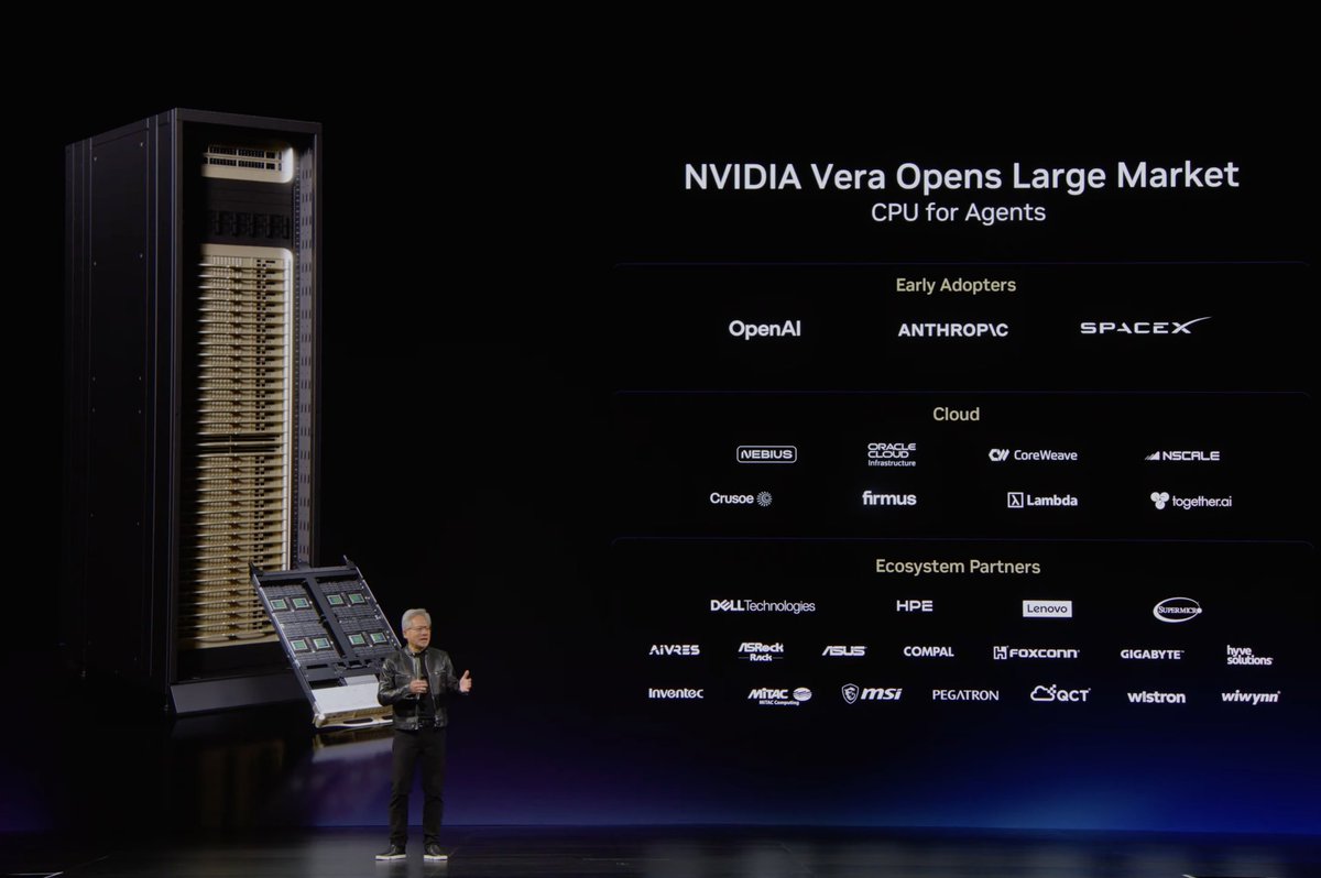
Jensen named OpenAI, Anthropic, and SpaceX as early Vera adopters. Storage scales with every rack they deploy.
$SNDK: 78% gross margin, $42B in committed contracts, enterprise SSD now 25% of portfolio.
The market is pricing NAND as a commodity.
Agentic workloads aren't.
Jun 1

Nvidia $NVDA CEO Jensen Huang just said we are at the beginning of a new market
CPUs FOR AGENTS
Here's who is already signed up to use Nvidia's new Vera CPU:
EARLY ADOPTERS:
- OpenAI
- Anthropic
- SpaceX $SPCX
CLOUD PARTNERS:
- Nebius $NBIS
- Oracle Cloud $ORCL
- CoreWeave $CRWV
- Nscale
- Crusoe
- Firmus
- Lambda
- Together AI
ECOSYSTEM PARTNERS:
- Dell Technologies $DELL
- HPE $HPE
- Lenovo
- Super Micro Computer $SMCI
- Aivres
- ASRock Rack
- Asus
- Compal
- Foxconn
- Gigabyte
- Hyve Solutions
- Inventec
- Mitac Computing
- MSI
- Pegatron
- QCT
- Wistron
- Wiwynn
122
$MRVL confirmed: 1.6T products in production delivery, not qualification.
Two T&M markets exist in optics.
$KEYS earns high-ASP revenue when a bandwidth generation is being certified; the 1.6T qualification cycle ran through 2025.
$VIAV earns production-floor revenue when the same generation ships at volume 4 test insertions per production line, scaling with every unit.
Keysight's 1.6T cycle is over. Viavi's just started.
$LITE, $COHR, $AAOI , $FN are all ramping 1.6T now. Every unit flows through Viavi instruments.
Viavi's Q4 2026 inflection is the readthrough nobody modeled.
27 May 2025

JPMorgan Reiterates Overweight Rating on $MRVL, Maintains PT at $130
Analyst comments: "Marvell is set to report earnings Thursday, and we expect a continued volume ramp of its two large AI ASIC programs (Amazon Trainium 2 ASIC/Google Axion ARM CPU), strong demand for its 800G products, and the initial ramp of 1.6T optical DSPs. This is combined with a continued cyclical recovery in its enterprise and carrier segments. Overall, we expect April-quarter results (we estimate $1.875 billion, up 3% quarter-over-quarter) and July-quarter guidance (we expect $2.00 billion , up 7% quarter-over-quarter) to be in line with JPMorgan and consensus estimates, with solid datacenter growth led by its AI ASIC ramps, growth in 800G/1.6T AI optical shipments, 400ZR shipments, and HDD/SSD controllers. The remainder of its business should also show sequential growth driven by cyclical improvements and new product cycles.
Recall that the team reaffirmed its April-quarter revenue outlook in early May. Since then, we believe accelerated compute demand remains strong, as indicated during earnings season from cloud and hyperscaler capex spending and AI infrastructure beneficiaries (e.g., MTSI, ALAB). On custom ASICs, the team continues its production ramp at Amazon with the Trainium 2 AI XPU ASIC, and as we recently highlighted, we believe Marvell’s Trainium 3 (3nm) program at AWS is progressing well and is on track to ramp in calendar year 2026 in high volumes. We also believe Marvell’s Microsoft AI ASIC MAIA Gen 2 (3nm) program is on track for a CY26 ramp, and Marvell has already won the Gen 3 MAIA (2nm/3nm chiplet – 3DSOIC) program, with production planned for a CY27/28 ramp.
Within the optical business, 800G PAM4 optical DSP orders and shipments remain solid, with an increasing ramp of next-gen 1.6T DSP into the second half of the year. Overall, we estimate the team will drive $4 billion in total AI ASICs and networking revenues this year. In the cyclical business, demand from enterprise networking (Cisco) remains healthy, and demand in carrier infrastructure is stabilizing. In automotive, the divestiture of the auto business, expected to close in CY25 ($225–$250 million revenue in FY26), is a revenue headwind but should be accretive to earnings by $0.05–$0.10, assuming proceeds are used for share repurchases.
More importantly, we see the team’s custom datacenter and AI ASIC pipeline continuing to expand (SmartNIC/DPU ASIC chips, HBM4 base die controller ASICs, eSSD controller ASICs, follow-on AI accelerator ASIC wins). We maintain our Overweight rating, as we see the team’s AI ASIC, optical, cloud, and storage segments continuing to drive solid growth while cyclical 5G and enterprise businesses recover."
Analyst: Harlan Sur
425
$MRVL: pluggable 70% YoY, data center interconnects doubling to $1B, cluster optics tripling to >$300M.
All simultaneously.
This isn't three tailwinds. It's one.
Traditional AI: one query, one response.
Agentic AI: plan → tools → memory → sub-agents → synthesis.
That's 10-50 model calls per task, many crossing data centers.
Every optical demand line is downstream of that multiplier.
The laser supply behind all three: $LITE, $COHR,
$AAOI.
Already sold out.
194
Every time $NVDA drops an open-weights model, the conversation is about the model.
The money is in the infrastructure.
550 billion parameters. Every enterprise that wants a custom version fine-tunes it on its own data.
That takes a real cluster, not a consumer GPU, not a cloud API.
That demand flows to $IREN $CRWV $NBIS.
Open weights enterprise fine-tuning = structural GPU rental demand that doesn't get priced at launch.
Watch neo-cloud utilization in earnings. That's where Nemotron shows up.
72
The AI silicon war has exactly one company with no losing scenario: $MRVL
Custom ASIC wins: Marvell designed them. $NVDA GPUs win: Marvell XPUs run inside the same NVLink clusters.
Either way, every optical module connecting to any of them runs Marvell's DSP at ~70% market share.
The duopoly with $AVGO in custom silicon design services isn't a competition; both are fully booked across all four hyperscalers simultaneously.
More total AI silicon investment expands both businesses in parallel.
120
Samsung has no reason to fix the conventional DRAM shortage. Here's why.
At 90-95% DRAM prices, Samsung's semiconductor business runs at peak margins. Samsung's mobile business absorbs the higher memory cost, but at the corporate level, the two roughly offset.
Adding supply would compress the pricing that makes the semiconductor unit profitable. Withholding it keeps the margin premium intact.
The world's largest DRAM producer is also the world's largest DRAM buyer. That's not a supply relief valve. That's a structural ceiling. Other producers benefit from Samsung's rational inaction.
110
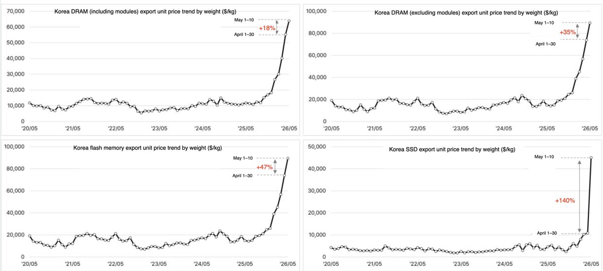
DRAM contracts 90-95% QoQ.
Who captures that pricing without spending billions converting to HBM?
Nanya Technology.
Pure-play conventional DDR4/DDR5. No HBM exposure. No TSV CapEx.
Just a DRAM producer in a market that repriced 90-95% because its three largest competitors allocated capacity to AI instead.
$SNDK invested $1B in Nanya in 2026. That position is now sitting inside one of the most favorable conventional DRAM pricing environments in history.
1
140
Conventional DRAM prices just became one of the best real-time AI capex indicators available.
GPU production pulls HBM capacity from shared DRAM fabs.
Less capacity for conventional → prices spike.
The conventional DRAM price sits downstream of the HBM allocation decision, which sits downstream of GPU production rates.
When it reverses, it won't read as "consumer electronics softness." It'll be an early signal that $NVDA or $AMD shipment velocity is slowing weeks before sell-side picks it up.
90-95% QoQ says AI production is still running full.
92
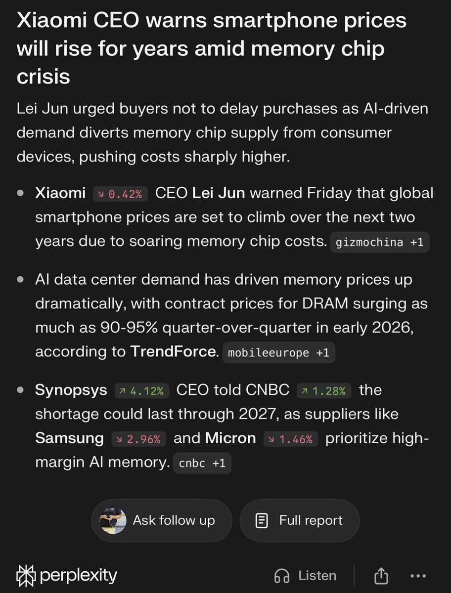
DRAM contract prices 90-95% QoQ. Xiaomi just raised phone prices by $29.
This isn't a consumer demand story.
Every $NVDA Rubin NVL72 rack contains 72 GPUs × 12-16 HBM dies. Each die requires a Through-Silicon Via etch on $LRCX Syndion systems.
That fab time doesn't simultaneously produce LPDDR5X for smartphones.
AI is diverting the memory supply.
The capacity that was used to build handset DRAM now builds HBM for data centers.
Xiaomi absorbs the cost at the other end.
The constraint lives in $LRCX lead times, not in consumer spending.
May 23
XIAOMI CEO WARNS SMARTPHONE PRICES WILL KEEP RISING
Lei Jun says smartphone prices are likely to climb over the next two years as memory chip costs rise.
The pressure is coming from AI data-center demand pulling supply toward higher-margin memory products.
TrendForce says conventional DRAM contract prices rose 90%-95% QoQ in Q1 2026.
NAND flash prices rose 55%-60% in the same period.
Xiaomi already raised prices on several handset models earlier this year by about $29.
The AI memory shortage is no longer just a data-center problem.
It is starting to show up in phones, PCs, consoles and other consumer electronics.
2
200
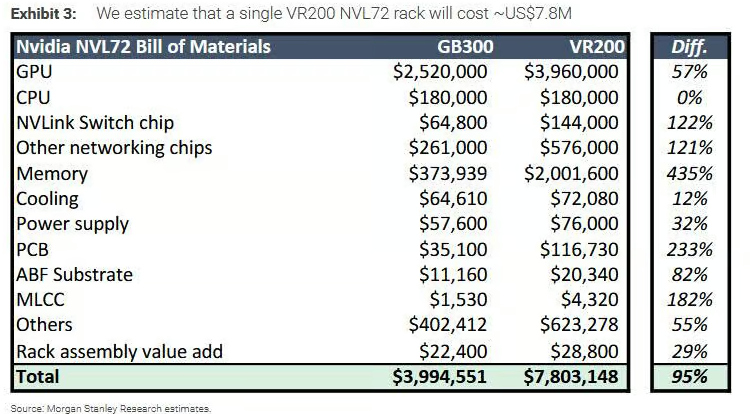
$TTMI is the most overlooked name in the Rubin NVL72 story.
The 44-layer midplane didn't exist in the previous GPU generation. $27K per rack.
New product class. $DELL can't ship an NVL72 without it.
$46K of the per-rack PCB uplift is structural new categories, not a price increase on existing boards. Revenue that was zero in GB300.
Aerospace qualification heritage puts you at the front of the line for new product classes.
Dell just ran L11 stress tests on these boards. They passed.
$51B in AI server backlog. This math is quiet. That's the point.
Too many people have been asking me why TTMI is up in pre-market, so I’ll answer it this one time. Next time, please look it up yourselves.
PCB stocks surged sharply in the Chinese market today.
The reason PCB names rallied in China is that Morgan Stanley analyzed NVIDIA’s next-generation Rubin rack and found that the rack ASP could reach roughly $7.8 million, almost doubling from GB300. More importantly, Morgan Stanley argued that this value uplift does not mainly come from the GPU itself, but from components such as PCBs ( 233%), MLCCs ( 182%), and ABF substrates ( 82%), which are expected to be the biggest beneficiaries.
As a result, several PCB supply-chain names rallied sharply, including:
Ding Tai Gao Ke (301377.SZ): 20%, limit-up
The global No. 1 player in micro-drills and routers used in the drilling process, a critical step in PCB manufacturing.
Shenghong Technology (300476.SZ): 13.3%
and other PCB supply-chain companies.
385
$INTC now has $MSFT (Maia 2 committed), $AMZN (early), $AAPL (preliminary), $NVDA / $AVGO (evaluation), and xAI/ $TSLA exposure.
This is the strongest external customer pipeline Intel Foundry has shown since the pivot.
Intel is slowly turning the foundry story from hope into reality.
May 8
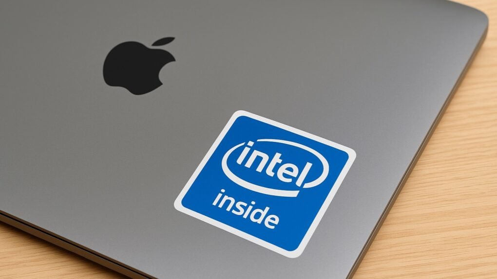
APPLE AND INTEL REACH PRELIMINARY CHIP-MAKING AGREEMENT
WSJ reports $AAPL and $INTC have reached a preliminary agreement for Intel to manufacture some chips for Apple devices.
It is still unclear which Apple products Intel would make chips for.
The Trump administration reportedly pushed for the deal, with Commerce Secretary Howard Lutnick meeting Apple, Nvidia, Musk, and others to bring them into Intel’s ecosystem.
Intel now has partnerships with Apple, Nvidia, and Musk-linked companies.
Washington is trying to turn Intel Foundry into a U.S. chipmaking platform for America’s biggest tech companies.
638
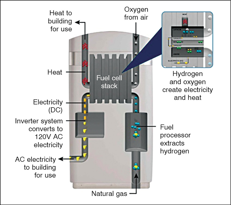
The full AI infrastructure chain just closed in one event.
$BE powers $CRWV with on-site SOFC fuel cells. $2.6B supply agreement.
$DELL just delivered Rubin NVL72 racks at CoreWeave. 72 Rubin GPUs.
Liquid-cooled. L11 stress-tested.
→ On-site SOFC power
→ Liquid-cooled GPU racks
→ AI inference revenue
This is what the grid bypass thesis looks like when it materializes. Grid queue too slow. SOFC in 55 days. Rubin deployed.
May 31

$DELL delivered the world’s first $NVDA Vera Rubin NVL72 rack to $CRWV marking the first confirmed shipment of Nvidia’s next-gen AI rack system.
The system includes 72 Rubin GPUs, 36 Vera CPUs, 3.6 exaFLOPS of FP4 inference, 75TB of fast memory and 260TB/s of NVLink bandwidth.

1
1,224
The Nexus program uses $TSM CoWoS advanced packaging and high-speed optical interconnects.
This adds another large, committed demand layer for $BESI hybrid bonding and die-attach tools, as well as $LITE / $COHR InP EML lasers and $FN CPO assembly.
The advanced packaging and optical bottleneck just got wider and longer.
May 7
"The companies are negotiating an agreement for $AVGO to finance the first phase of chip production, which would consume 1.3 GW of data center capacity and would cost around $18B. At that rate, the full 10 GW program, code-named Nexus, could cost $180B in chip production alone before factoring in data center construction and other costs."
2
604
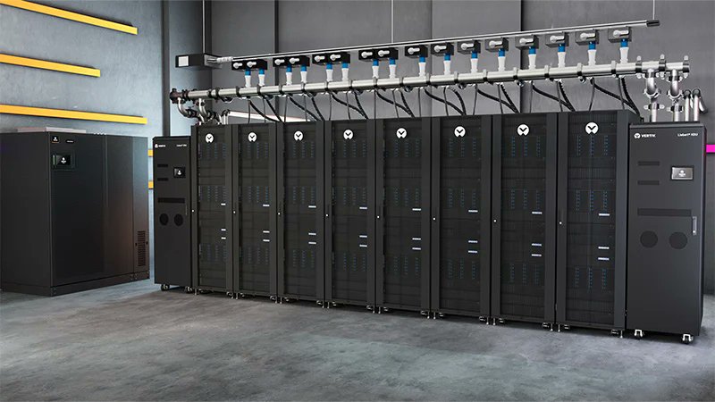
AI servers now require dedicated CPU racks for agentic orchestration.
This creates an entirely new demand layer for power and cooling infrastructure.
$VRT is one of the clearest beneficiaries of this shift.
The AI power infrastructure thesis just got another strong, named corroboration.
1
344
$ARM delivered the strongest confirmation yet for its data center CPU business.
$2B committed demand for AGI CPUs, “4× CPU capacity” for agentic AI, and management openly admitting they “under-called” the demand.
ARM is no longer a mobile royalty company.
It is becoming a core structural beneficiary of the entire AI buildout.
2
533
$NVDA partnered with $GLW to build 10x US optical connectivity capacity for AI data centers.
This is a massive, named commitment to US-made optics.
$AAOI is the only TAA-compliant US manufacturer of 800G/1.6T transceivers at scale.
The US optical supply chain just got NVIDIA’s direct endorsement and AAOI sits right at the center of it.
1
8
1,311