
Total Investment Reaches €1.5–2.0 Billion! AMD and Global Substrate Major Expand AI Substrate Project in Southeast Asia...ic-pcb.com/total-investment-…
@ATS_AG #AMD #AISubstrate #ICSubstrate #AdvancedPackaging #SemiconductorIndustry #AIHardware #MalaysiaManufacturing #PCBIndustry

1

$ONTO | Morgan Stanley Initiates Overweight – PT $371
Key Points:
Morgan Stanley initiates coverage on Onto Innovation
Rating: Overweight
Price target: $371
Analyst sees potential for earnings upside and valuation re-rating
Growth Drivers:
Advanced Node Exposure:
Revenue growth estimated at 30% (2026) and 39% (2027), outpacing WFE growth
Advanced Packaging:
Strong growth in Specialty Device & packaging segment
Expansion driven by Dragonfly G5 and Semilab integration
High-Margin Expansion:
Gross margin projected to rise from ~54.6% → ~58% by 2027–2028
Supported by manufacturing shift and higher software mix
Additional Upside Optionality:
“Moonshot” products (Echoscan, 3Di, PLP) each potentially becoming meaningful revenue contributors
Takeaway:
Morgan Stanley views Onto Innovation as a high-growth semiconductor process control beneficiary of AI-driven leading-edge manufacturing, with both earnings acceleration and multiple expansion potential.
#ONTO #OntoInnovation #Semiconductors #AI #WFE #AdvancedPackaging #MorganStanley
26
Samsung Electronics is considering Saemangeum for a massive advanced packaging plant to scale HBM capacity and challenge TSMC. Front-end logic node scaling is zero-sum without physical back-end packaging on domestic soil. #AdvancedPackaging Source: kedglobal.com/korean-chipmak…
14
1/ Nobody talks about the real bottleneck in advanced AI packaging. It is not what you think. It's the physical construction of back-end facilities. @Samsung mulls a massive chip packaging plant on Saemangeum to scale HBM4 capacity. #AdvancedPackaging
1
4
Google is reportedly in talks with Samsung to make its next-gen 'Icefish' TPU to break TSMC's packaging monopoly. Silicon dominance is no longer gated by design, but by who controls advanced HBM and substrate integration. #AdvancedPackaging Source: forbes.com/sites/johnwerner/…
8
5/ Design is useless if you cannot package and measure your custom silicon. Fabs are a paper victory if you don't secure the advanced material deposition, sub-nanometer metrology, and the packaging lines on regional soil. #AdvancedPackaging
1
1

TSMC's advanced packaging capacity has become one of the AI industry's most binding constraints, with demand so far ahead of supply that the chip giant is now routing overflow orders to Taiwanese partners — most notably ASE Technology Holding and Powertech Technology — who are racing to scale up alongside TSMC to capture growth from AI and high-performance computing.
TSMC CEO C.C. Wei has publicly acknowledged that CoWoS capacity remains extremely tight and is effectively sold out through 2026. Analysts project TSMC's monthly CoWoS capacity will roughly expand from 70,000 wafers at the end of 2025 to 115,000 wafers by the end of this year, with TSMC reportedly converting some of its older 8-inch wafer fabs in Taiwan into advanced packaging facilities to help close the gap. As its most advanced packaging lines run at full capacity, TSMC has shifted part of its advanced packaging orders to outsourced semiconductor assembly and test (OSAT) firms rather than letting customer demand go unmet.
ASE is a major beneficiary of this spillover. Beyond expanding its own CoWoS back-end packaging capacity, ASE has the potential to secure direct front-end CoW process orders from Broadcom, NVIDIA, AMD, and Amazon this year, with its CoWoS capacity target expected to double. ASE itself is projecting its advanced packaging sales to double in 2026 as TSMC continues offloading sub-steps of the CoWoS process to relieve its own backlog.
Powertech, meanwhile, is positioning a proprietary alternative technology to capture demand directly. The company has developed PiFO, an advanced packaging technology benchmarked against TSMC's CoWoS-L, which has already won large orders from multiple U.S. AI chip firms — with most of its 2026 advanced packaging capacity already booked and strong demand expected to continue through 2027. Unlike CoWoS's round silicon interposer, PiFO uses a square panel-level design with a glass substrate, offering better heat dissipation and roughly 30% lower production costs. To meet this demand, Powertech plans to nearly double its capital spending to a record NT$40 billion in 2026, and its position as the world's leading memory packaging and testing provider gives it strong ties across major DRAM and NAND manufacturers — a strategic advantage for next-generation AI packaging.
The bigger picture is one of structural realignment across the supply chain. The concentration of advanced packaging capacity in Taiwan represents a significant systemic risk for the global AI industry, and the overflow from TSMC has created a meaningful opportunity for OSAT providers like Powertech and ASE to step in with CoWoS-like solutions. The surge in demand is being driven in part by major tech firms such as OpenAI and Amazon, who are partnering with Broadcom and other ASIC designers to develop in-house AI chips — further intensifying competition for both advanced process and packaging capacity.
#TSMC #ASE #Powertech #CoWoS #AdvancedPackaging #AIChips #HPC #Semiconductor #NVIDIA #AMD #ChipShortage #TaiwanTech #AIInfrastructure #ChipManufacturing
1
1
57

20h
AI COMPONENT TRIPLE PLAY: iM SECURITIES RAISES SAMSUNG ELECTRO-MECHANICS TARGET 28%
TLDR: Samsung Electro-Mechanics is gaining upside across three AI hardware bottlenecks at once — MLCC pricing, fully utilized FC-BGA capacity and new silicon-capacitor demand from advanced packaging.
iM Securities raised its target price by 28% and lifted 2027–2028 operating-profit estimates to 3.3 trillion won and 4.3 trillion won. MLCC pricing could beat the assumed 20% increase as Yageo pushes general-purpose hikes, Apple sustains stronger production and Nvidia’s Vera Rubin raises MLCC content per NVL72 rack to 500,000–600,000 units from 440,000. FC-BGA utilization is expected to hit 100% in the second half of 2026, while additional cloud-provider silicon-capacitor orders could trigger further earnings upgrades.
#SamsungElectroMechanics #Samsung #MLCC #FCBGA #SiliconCapacitors #AdvancedPackaging #NVIDIA #VeraRubin #Apple #Yageo #AIInfrastructure #Semiconductors #KoreaStocks #KoreaMarkets $SSNLF $NVDA $AAPL $EWY $KORU

1
2
13
1,049
20h
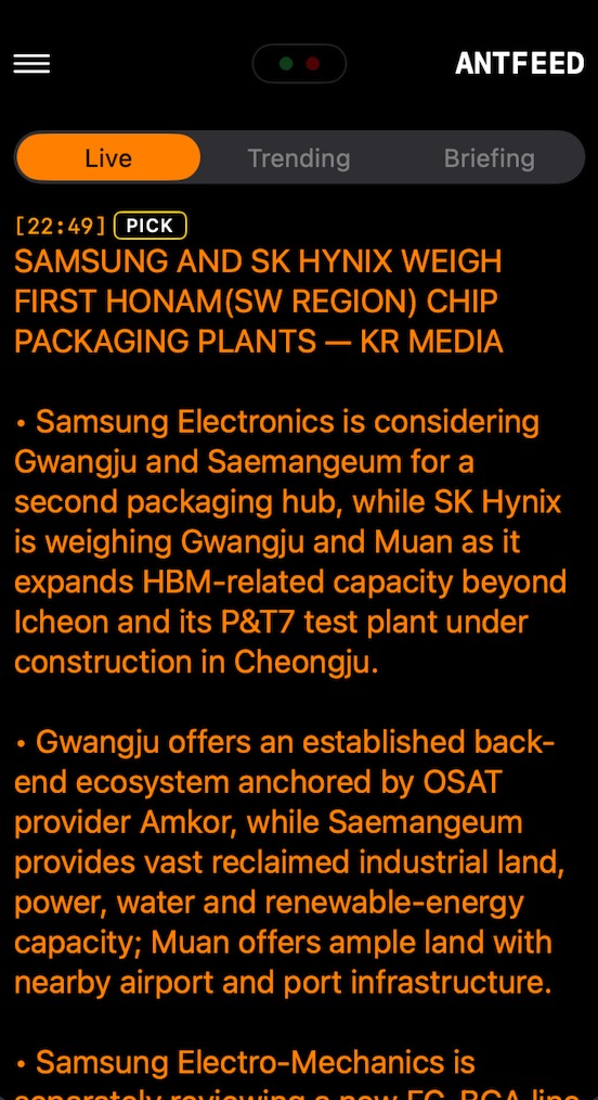
HONAM CHIP LAND GRAB: SAMSUNG AND SK HYNIX EYE FIRST PACKAGING HUBS IN SOUTHWEST KOREA
TLDR: Korea’s next semiconductor expansion may shift toward regional packaging clusters, with Samsung and SK Hynix weighing new Honam hubs while Samsung Electro-Mechanics considers an FC-BGA line in Sejong for a "North American Big Tech" customer.
Samsung Electronics is considering Gwangju and Saemangeum for a second packaging hub, while SK Hynix is weighing Gwangju and Muan as it expands HBM-related backend capacity beyond Icheon and Cheongju. Separately, Samsung Electro-Mechanics is reviewing a new FC-BGA line in Sejong for a "North American Big Tech customer", reinforcing the broader push into advanced packaging and substrates.
#Samsung #SamsungElectronics #SKHynix #SamsungElectroMechanics #Gwangju #Saemangeum #Muan #Honam #AdvancedPackaging #ChipPackaging #HBM #FCBGA #Amkor #KoreaSemis #KoreaMarkets $SSNLF $HXSCF $AMKR $NVDA $EWY $KORU $SMH $SOXX
135
Jun 14
AI PACKAGING GOLD RUSH: SAMSUNG ELECTRO-MECHANICS WINS $1B COMPONENT ORDER
TLDR: As AI packages become denser and lower-voltage, silicon capacitors are emerging as a new bottleneck component where Samsung Electro-Mechanics can expand beyond traditional MLCCs.
Samsung Electro-Mechanics secured a 1.5T won($1.0B) contract from a major global customer for silicon capacitors used to stabilize power and suppress noise inside GPU and HBM packages, targeting ultra-compact spaces where conventional MLCCs cannot fit.
#Samsung #SamsungElectroMechanics #SiliconCapacitors #MLCC #GPU #HBM #AIChips #AdvancedPackaging #Semiconductors #MemoryChips #KoreaSemis #KoreaMarkets #Nvidia $SSNLF $NVDA $HXSCF $MU $DRAM $EWY $KORU $SMH $SOXX

1
1
109

Jun 13
ASE Technology raised its 2026 LEAP advanced packaging outlook to over $3.5B, while Lam Research expects packaging revenues to surge over 50% in 2026. Design is useless without physical advanced packaging capacity. @semianalysis @ASML_News #AdvancedPackaging Source: au.finance.yahoo.com/news/as…
1
17
Jun 13
4/ To support this, ASE is investing an additional $600M in machinery for advanced wafer sorting. This matches Lam Research’s announcement today that it anticipates advanced packaging revenue growth to exceed 50% in calendar year 2026. #AdvancedPackaging
1
8
Jun 13
Park Systems secured KRW 100 billion to scale Atomic Force Microscopy (AFM) manufacturing. As advanced 3D packaging and 2nm nodes grow more complex, sub-nanometer surface metrology is the ultimate yield gatekeeper. #AdvancedPackaging Source: azonano.com/news.aspx?newsID…
13
Jun 13
1/ As advanced semiconductor nodes shrink to 2nm and adopt complex 3D-IC packaging, traditional optical inspection is hitting a hard physical wall. You cannot yield what you cannot measure. Sub-nanometer metrology is the hidden gatekeeper. @semianalysis #AdvancedPackaging
1
14

Jun 13
$MU HBM ほとんど知られていない事実:マイクロンのAIメモリはボイシからアジアへ世界的なルートを取る
TLDR:マイクロンのHBM戦略は地理的に分かれている — 米国のR&D、日本でのウェハ製造、アジアのバックエンド生産能力 — これにより、すべてのボトルネックを一国に集中させることなくスケールアップが可能。
マイクロンはボイシで次世代HBMアーキテクチャとプロセスを開発、広島で先進メモリウェハを製造し、組み立て、先進パッケージング、テストの多くを台湾に依存している。東広島の新しい96億ドルのHBM施設とシンガポールの70億ドルの先進パッケージング工場が、フロントエンド製造とバックエンド生産能力の両方を拡大する。
#Micron #HBM #HBM3E #HBM4 #MemoryChips #DRAM #Semiconductors #AdvancedPackaging #Boise #Hiroshima #Taiwan #Singapore #AIChips #AIInfrastructure $MU $NVDA $AMD $AVGO $TSM $SMH $SOXX $DRAM
Jun 13

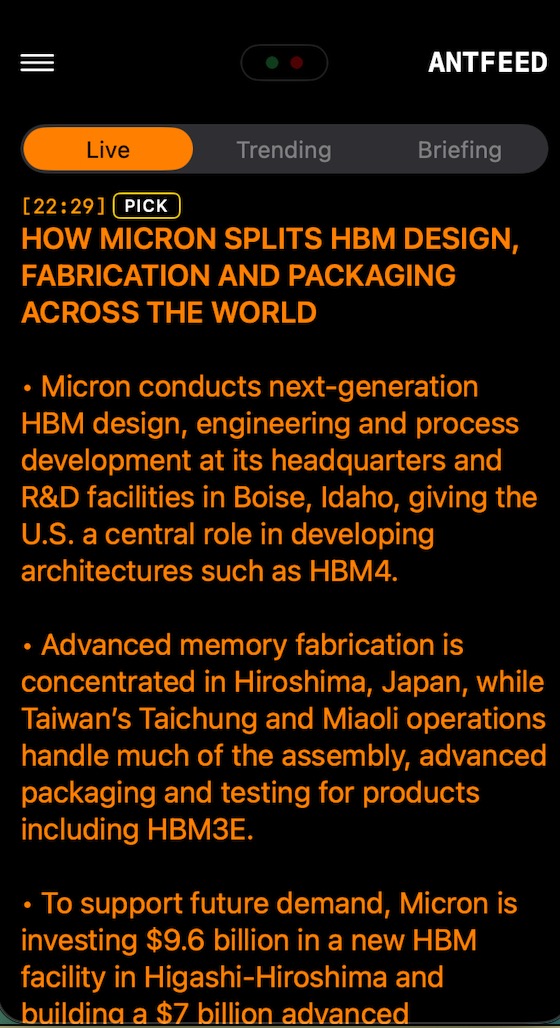
$MU HBM FACT FEW PEOPLE KNOW: MICRON’S AI MEMORY TAKES A GLOBAL ROUTE FROM BOISE TO ASIA
TLDR: Micron’s HBM strategy is geographically split — U.S. R&D, Japanese wafer fabrication and Asian backend capacity — allowing it to scale without concentrating every bottleneck in one country.
Micron develops next-generation HBM architectures and processes in Boise, fabricates advanced-memory wafers in Hiroshima, and relies on Taiwan for much of the assembly, advanced packaging and testing. A new $9.6B HBM facility in Higashi-Hiroshima and a $7B advanced-packaging plant in Singapore will expand both front-end fabrication and backend capacity.
#Micron #HBM #HBM3E #HBM4 #MemoryChips #DRAM #Semiconductors #AdvancedPackaging #Boise #Hiroshima #Taiwan #Singapore #AIChips #AIInfrastructure $MU $NVDA $AMD $AVGO $TSM $SMH $SOXX $DRAM
1
914
Jun 13
$MU HBM FACT FEW PEOPLE KNOW: MICRON’S AI MEMORY TAKES A GLOBAL ROUTE FROM BOISE TO ASIA
TLDR: Micron’s HBM strategy is geographically split — U.S. R&D, Japanese wafer fabrication and Asian backend capacity — allowing it to scale without concentrating every bottleneck in one country.
Micron develops next-generation HBM architectures and processes in Boise, fabricates advanced-memory wafers in Hiroshima, and relies on Taiwan for much of the assembly, advanced packaging and testing. A new $9.6B HBM facility in Higashi-Hiroshima and a $7B advanced-packaging plant in Singapore will expand both front-end fabrication and backend capacity.
#Micron #HBM #HBM3E #HBM4 #MemoryChips #DRAM #Semiconductors #AdvancedPackaging #Boise #Hiroshima #Taiwan #Singapore #AIChips #AIInfrastructure $MU $NVDA $AMD $AVGO $TSM $SMH $SOXX $DRAM
13
142
17,684

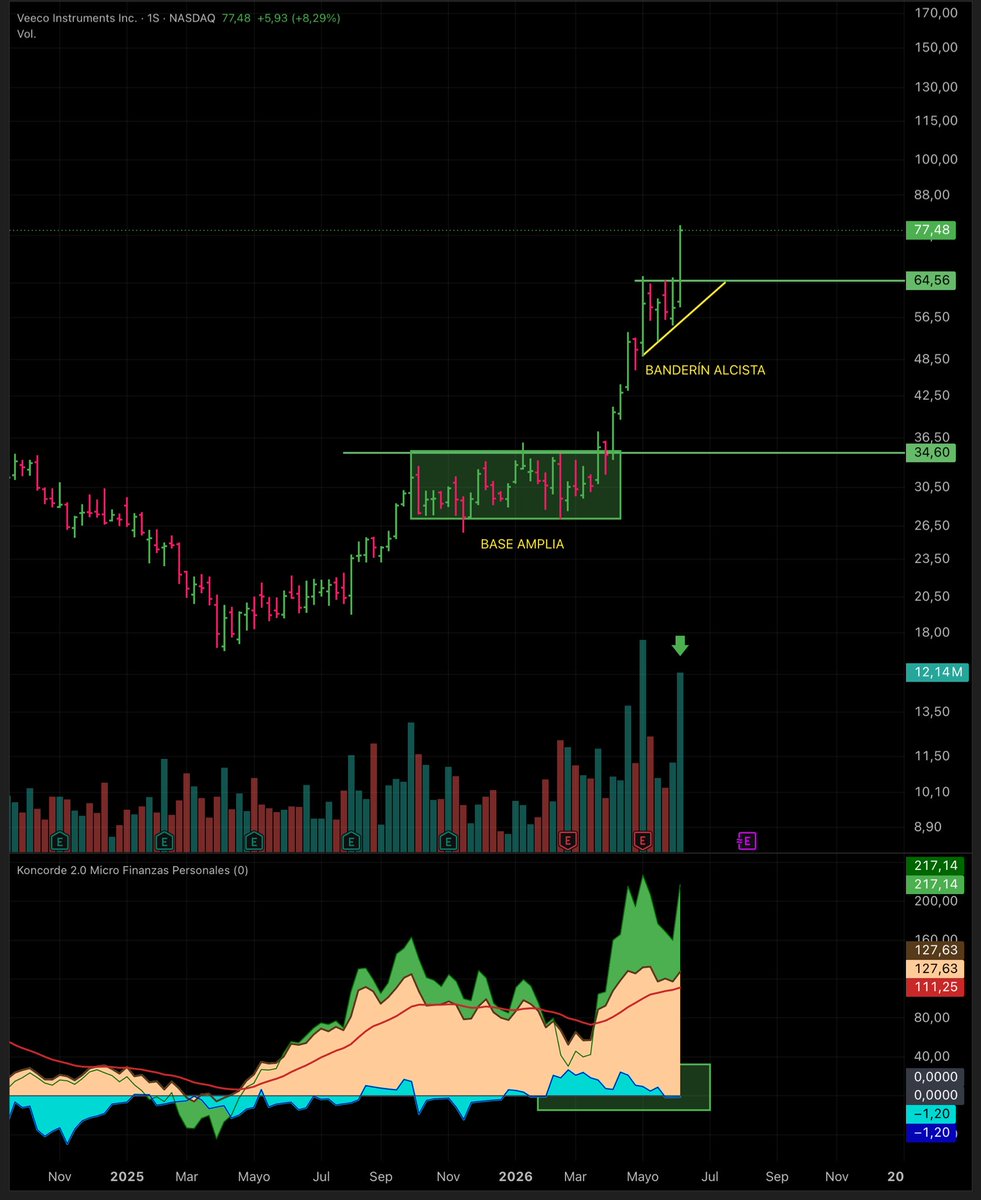
Jun 13
$VECO Buena semana para esta empresa del sector de semiconductores, rotura del banderín con casi el doble de volumen de la semana anterior, muy buen aspecto a nivel semanal, se nota que hay interés
#Semiconductors $NVDA #Microchips #AdvancedPackaging
43

Shape the future of tech! We’re excited to launch our PG Diploma in Semiconductor Device Packaging. Equip yourself with industry-ready skills to power the next gen of AI, smartphones & microelectronics. 💻🔬
#Semiconductors #AdvancedPackaging #Engineering

1
24

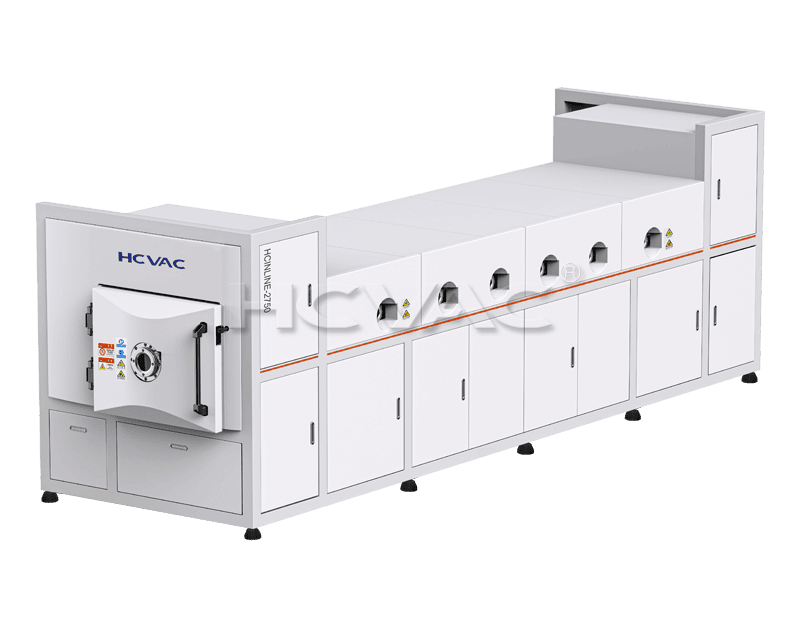
HCVAC's Deep Via Glass Sputtering technology supports seed layer deposition in TGVs with aspect ratios up to 15:1, helping enable next-generation glass substrate applications.
Learn more: hcvacuum.com/tgv-tcv-sputter…
#ThroughGlassVia #AdvancedPackaging #Chiplet #HBM #PVD #HCVAC

42
Jun 13
TSMC TAIWAN FORTRESS: 2NM, 3NM AND COWOS EXPANSION LOCKS IN THE AI CHIP CORE
TLDR: TSMC is widening capacity across leading-edge logic and advanced packaging at the same time, making Taiwan even harder to displace as the central production hub for the AI semiconductor stack.
TSMC is expanding 2nm capacity in Hsinchu and Kaohsiung, 3nm production at Tainan Fab 18, and CoWoS and SoIC packaging at Chiayi AP7 and Southern Taiwan Science Park AP8 to meet demand from Nvidia, AMD, Broadcom and custom-ASIC cloud providers, while Marketech International and other suppliers build out the supporting equipment, materials, engineering, substrate and testing ecosystem in Pingtung.
#TSMC #TaiwanSemis #2nm #3nm #CoWoS #SoIC #AdvancedPackaging #AIChips #Semiconductors #Nvidia #AMD #Broadcom #CustomASIC #CloudAI #MarketechInternational $TSM $NVDA $AMD $AVGO $SMH $SOXX

1
173