

Jun 12
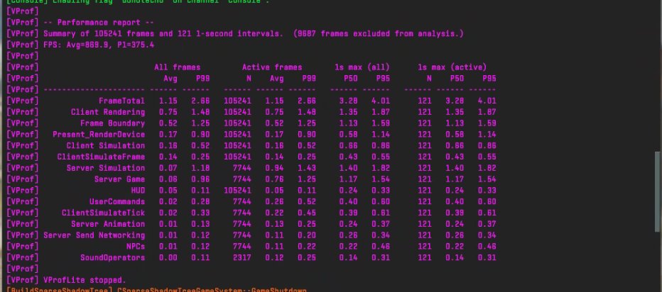
CS2 loves higher negative CO values.
This is a 9800X3D with -20 offset and further BIOS/OS tuning BUT higher CO values will throw FCLK instability very quickly.
You must re-validate with linpack and y-cruncher again.
A good reminder that you must not rely on a benchmark result because it looks good!
19
3
145
19,297

Jun 8
Let's see...
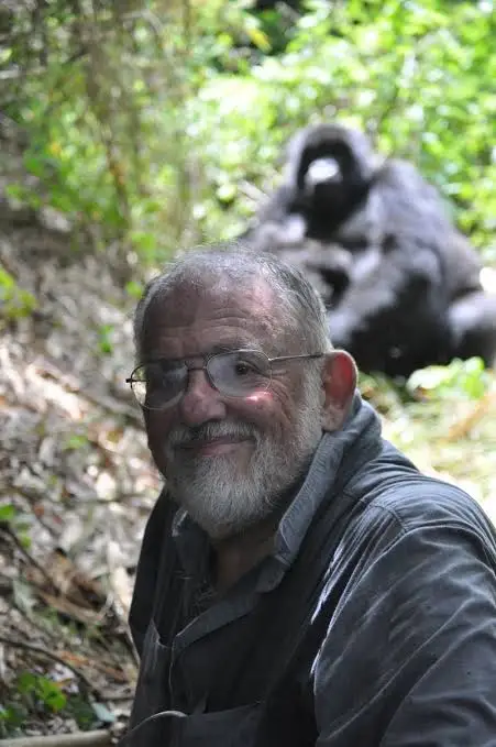
California is home to Lawrence Livermore National Laboratory. They have El Capitan, currently the world's fastest supercomputer.
As of the latest TOP500 rankings (November 2025 data), it achieves an Rmax of 1.809 exaFLOPS on the High Performance Linpack (HPL) benchmark.
That's roughly 1.8 quintillion calculations per second.
Yet, somehow, LA takes a month to count votes.
Sounds legit. 🤬
1
29

Bitcoin is also backed by specialized supercomputing. I estimate that the world's fastest computer, El Capitan at the Department of Energy's Lawrence Livermore Laboratory, used for nuclear weapons stockpile stewardship but also fusion power research, astrophysics research, and materials science research,
and
possessing a peak floating rate of 1.7 Exaflops on Linpack (matrix multiplication mostly) and consuming 30 Megawatts,
by my estimate would only produce of order a couple of Petahashes/sec for Bitcoin mining, or less than 4 state of the art ASIC mining rigs.
Bitcoin ASICs are multi-module, highly pipelined, and very highly parallel in replicating functional units, and also gain enormous advantage because they:
* hardwire the exact dataflow,
* eliminate instruction decode,
* eliminate caches,
* eliminate memory hierarchy overhead,
* eliminate branch/control logic,
* deeply pipeline the exact rotate/XOR/add structure,
and maximize hashes/Joule rather than generic ops/sec.
El Capitan would be a smallish fraction of 1% of the Zettahash/s produced by the world's largest decentralized supercomputing network.
@ShahinKhan
Jun 4

"Bitcoin isn't backed by anything."
Let me stop you right there.
Bitcoin is backed by energy. Real energy. Kilowatts. Heat. Physics.
The kind of backing you can't print, fake, or vote into existence at an emergency Fed meeting.
Every block mined is a thermodynamic proof of work. Not a promise. Not a policy. Proof.
The issuance schedule has never been amended by a committee. Not once. Not ever. Because there is no committee.
There's just math. Cold, indifferent, and immune to political theater.
The network is secured by more raw computing power than anything humanity has ever built. Hundreds of exahashes per second standing guard. Every single day.
Now let's talk about what is backed by nothing.
The dollar.
It's is backed by confidence. Specifically, confidence in the institution that printed $6 trillion in two years while telling you 3% inflation was healthy and you should be grateful for the soft landing.
In the same people who can't pass an audit.
Who fund wars with a credit card.
Who promise solvency while sitting on $39 trillion in debt and accelerating.
"Backed by nothing" isn't an attack on Bitcoin.
It's a confession about the dollar.
Follow if you're serious about building wealth they can't print away.
4
7
53
7,920

Lowkey if it passes 20 runs of Linpack it's probably stable
1
5
312

May 28
Cleve Moler博士が2026年5月20日、86歳で逝去されました。心よりご冥福をお祈りいたします。彼はFortranが科学技術計算の絶対的標準だった1970年代後半、学生たちがLINPACKやEISPACKを「プログラミングせずに」簡単に使えるようにという思いから、MATLABの原型をFortranで作りました。それが後に「計算の民主化」を象徴するツールへと育っていきます。1984年、Jack Littleらと共にMATLABをC言語で全面的に書き直し、MathWorksを設立。PC時代に対応した商用版をリリースしたことで、世界中の研究者・エンジニアが行列演算や数値解析を直感的に扱える環境が広がりました。以降、ツールボックス、Simulink、グラフィックス、さらには現代のNumPy/SciPyやJuliaにも影響を与えるほどの巨大なエコシステムへと発展。プログラミングの専門家でなくても科学を加速できる「道具」を提供し続けた功績は計り知れません。Cleve Moler博士の遺した哲学——「コードを書く手段ではなく、発見を加速させる道具」——は今も生き続けています。本当にありがとうございました。安らかにお眠りください。#CleveMoler #MATLAB #数値計算 #科学技術計算 #NumericalComputing
2
3
1,693


RIP Cleve Moler. His LINPACK code died some time ago, but his decisions about Matlab were inherited in Torch and are thus reified thousands of times per second.
1
2
23
1,309

May 26
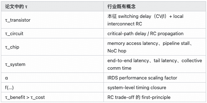
Huawei’s “Tao / τ Law”: Tech Paper, White Paper, or Strategic Manifesto? 🧠🚀
🌟Insights from Zhihu contributor 无我梦中
Huawei’s new paper, “A Time Scaling Theory for Multi-Layer Electronic Systems” by Tingbo He, is better read as a semi-technical white paper strategic declaration, not as a pure theoretical research paper.
The core idea is powerful:
Replace “transistor size in nm” with “time constant τ” as the unified progress metric for semiconductors.
In plain English:
The future of chips is not only about making transistors smaller. It is about making the whole system wait less.
📌 What the Paper Is Really Saying
The paper’s logic can be summarized like this:
1️⃣ Moore’s Law was never just about space.
Smaller transistors mattered because they reduced time: faster switching, shorter wires, fewer boundaries, lower system delay.
2️⃣ After 7nm, geometric scaling gets weaker.
Intrinsic device delay no longer improves as easily. Local interconnect RC delay becomes more important. EUV depreciation, mask cost, verification, and design cost rise sharply. The cost-per-transistor curve is flattening or even turning upward.
3️⃣ So the industry should scale time directly.
Huawei defines τ across 12 orders of magnitude — from transistor picoseconds to data-center seconds — as a shared optimization target.
4️⃣ Huawei gives three major proof points:
• LogicFolding on Kirin 2026: 55% density, 41% energy efficiency, 13% frequency at the same node
• Unified Bus for AI data centers: remote access latency from tens of μs to ~100 ns
• Hi-ONE optical I/O 3D Folding: solve the 2.5D packaging “N² vs N” bottleneck
5️⃣ Long-term roadmap:
• by 2031: “equivalent 1.4nm” density, 400 MTr/mm²
• by 2035: 100× AI hardware integration
The direction is meaningful. But the details need careful reading.
1️⃣ The End of the Geometric Era
The paper starts with a familiar claim: geometric scaling is reaching its limit.
This is mostly true.
Cost-per-transistor no longer reliably falls. EUV depreciation eats a large share of wafer cost. High-end chip design budgets can approach or exceed $1B. IRDS, Hennessy & Patterson, and Horowitz have all made similar arguments.
For a company like Huawei, restricted by advanced lithography access, this wall arrives earlier and hits harder.
But here the paper mixes two things:
• the global slowdown of Moore-style economics
• Huawei’s own manufacturing constraints
TSMC N3/N2, Intel 18A, and Samsung GAA are still improving transistor density. The physical path is not fully broken. What is broken is the old economic contract: new node = better cheaper.
So the paper’s framing is selective.
It uses an industry consensus to make Huawei’s own solution look like the inevitable path forward.
That is understandable as strategy. But as pure industry analysis, it goes a bit too far.
2️⃣ Time, Not Space ⏱️
This is the most philosophical part of the paper.
Huawei argues that Moore’s Law benefited users not because chips became “smaller,” but because systems became faster.
So metrics like:
• frequency
• latency
• bandwidth
• throughput
are all treated as different expressions of τ at different layers.
This framing is useful. It gives process, circuit, architecture, system, and software teams a shared language.
But academically, it is not completely new.
Hennessy & Patterson’s “A New Golden Age for Computer Architecture,” Horowitz’s energy-per-operation work, and IRDS “More than Moore” roadmaps have all pushed the same direction: transistor shrinking alone is not enough; system-level optimization matters.
So τ scaling is more like a new name for an old system-level idea, not a new physical discovery.
There is also some looseness in the math.
Bandwidth is not a time constant. It is bits per time. Throughput is not simply 1/τ either; it should be closer to:
throughput = 1 / τ_per_op × parallelism
Parallelism gets quietly absorbed.
For management narrative, that simplification is fine.
For a paper claiming a Dennard-level full-stack target, it feels light.
The real value of this section is not theory. It is language. It gives the whole industry stack one number to talk about: time.
3️⃣ LogicFolding: The Most Concrete Part 🏗️
This is the section most likely to go viral.
Huawei uses Kirin 2026 as proof that LogicFolding can deliver big gains without changing the process node:
• transistor density: 155 → 238 MTr/mm²
• performance-core energy efficiency: 41%
• peak frequency: 13%
• SRAM frequency: 40%
• clock buffers: -50%
• clock skew: -25%
• wire length: -30%
On paper, this looks almost like gaining a full process generation.
The engineering details are also specific:
• hybrid bonding pitch: 1.5 μm
• overlay: under 0.5 μm
• TSV CD / KOZ: under 1.5 μm
• TSV pitch: under 6 μm
• failure rate: under 100 ppm
• with repair, yield close to 100%
None of these numbers are impossible. But each sits close to today’s hybrid-bonding limits.
The bigger issue is methodology.
The paper does not provide:
• die photos
• SEM images
• wafer-level yield curves
• clear PPA baselines
• workload details for energy efficiency
• test corner / voltage / temperature conditions
So the headline numbers are attractive, but hard to independently verify.
There is also an important density caveat.
The formula counts both active tiers into one footprint. So 238 MTr/mm² is package-footprint density, not true silicon-area density.
That is normal in 3D integration. It is not deception. But readers must understand what “density” means here.
It measures how efficiently packaging uses 3D space, not how small the transistor is.
What is LogicFolding really?
It is not just process innovation.
It is not just packaging innovation.
It is not a brand-new theory either.
It is a combined design methodology:
sub-2 μm hybrid bonding cross-die logic partitioning custom EDA flow
The direction is physically sound: shorten critical interconnects, improve density, frequency, and efficiency.
But before third-party measurement appears, it is safer to discount the exact numbers.
Believe Huawei probably built something real.
Do not treat every number like audited silicon data yet.
4️⃣ AI Data Centers: Unified Bus, Hi-ONE, 3D Folding 🌐
The paper then moves from one chip to AI clusters.
Unified Bus
Unified Bus tries to collapse today’s complex data-center communication stack.
Traditional AI clusters rely on layers like:
• PCIe
• NVLink or private fabrics
• Ethernet / InfiniBand
• RDMA software stack
• DMA buffers and handshakes
Every layer adds latency and copying.
Huawei’s Unified Bus wants to expose memory semantics across chassis, with hardware-managed consistency. The paper claims remote access latency improves from tens of microseconds to about 100 ns, or roughly 500× τ reduction.
This number needs caution.
“Tens of μs” sounds like a TCP/IP baseline. But modern AI clusters using RoCEv2 or InfiniBand already reach the 1–3 μs range across racks, and NVLink can go below 1 μs inside a rack.
So the chosen baseline is favorable.
The “~100 ns” claim is also unclear.
If it refers to on-package or rack-local fabric protocol latency, it may be reasonable. But if it refers to cross-rack physical distance, it violates basic propagation delay. Light in fiber needs about 500 ns one-way for 100 meters.
So the most reasonable reading is:
100 ns refers to rack-local fabric/protocol latency, not full cross-rack physical latency.
The paper does not clarify this enough.
Hi-ONE Optical I/O
Hi-ONE is Huawei’s near-package optical engine.
The paper mentions:
• 8 Tb/s per module
• electrical SerDes distance reduced from 100 cm to 5 cm
• optical path extended from under 1 m to 100 m
Technically, this direction is credible.
Broadcom CPO, TSMC COUPE, Ayar Labs, Lightmatter, and others are all moving in the 4–8 Tb/s range around this timeline.
Huawei’s choice of near-package optics is also practical. It is less aggressive than full co-packaged optics, but likely easier to engineer.
The missing pieces are key parameters:
• BER target
• pJ/bit
• thermal reliability
• laser MTBF
• single-mode vs multi-mode fiber
• cost structure
So the direction is industry-aligned. It is not obviously behind, but not clearly ahead either.
3D Folding and the N² vs N Problem
This is one of the strongest arguments in the paper.
In a traditional 2.5D AI chip:
• logic die sits in the center
• HBM, SerDes, and power delivery enter from the edge
If die side length is N:
Compute ∝ N²
because compute grows with area.
But:
Bandwidth / I/O / Power ∝ N
because they enter from the perimeter.
That creates a topology deficit. Compute grows faster than the ability to feed it.
This is not a Huawei-only observation. NVIDIA Blackwell, Marvell, TSMC, Apple, and others are all dealing with the same bottleneck. But Huawei explains it very clearly.
The 3D Folding solution is natural:
Move constrained resources from the edge to the surface:
• backside power
• integrated voltage regulation
• hybrid-bonded memory
• near-package optical I/O
• 3D stacking
Then bandwidth, I/O, and power can scale more like area.
I fully agree with the direction.
But the paper underplays the cost.
Stacking active tiers creates hard problems:
• lower-tier heat removal
• bond yield × known-good-die yield × bond yield
• hard post-bond fault diagnosis
• limited repairability
• hybrid bonding equipment cost
• CTE mismatch reliability
• TSV stress affecting channels
The paper lists these challenges later, but treats them optimistically. Thermal, yield, and test remain the hardest parts.
5️⃣ Logic and Memory Re-Fusion 🧠
This section is more industrial than academic.
For decades, logic and memory were deliberately separated. CPU focused on compute. DRAM focused on storage. Standard buses connected the two.
That worked well in the PC era.
But AI changes everything.
Model parameters, KV Cache, activations, and gradients make data movement as important as compute. HBM, hybrid bonding, 3D SRAM, near-memory compute, and in-memory compute all point to the same trend:
logic and memory must get closer again.
This is not new. AMD 3D V-Cache is already in production. HBM4 is coming. CXL explores memory pooling. Samsung, SK Hynix, Sony, and others are all moving in related directions.
The paper does not add much academic novelty here.
But the strategic message is strong.
When the paper says long-term success belongs to those who can fuse logic and memory technologically and economically, it is effectively calling upstream partners:
• CXMT
• YMTC
• Hua Hong
• SMIC
• Huawei’s own packaging ecosystem
The message is:
AI hardware winners must integrate logic, memory, packaging, and economics together. No one can optimize alone anymore.
6️⃣ Open Challenges: The Best Section ⚠️
This is the most credible part of the paper because it openly admits what is not solved.
EDA is the first bottleneck
Current EDA tools optimize area, timing, and power mostly in 2D.
LogicFolding needs tools that treat stacked dies as one continuous 3D design object:
• cell-level cross-die partitioning
• 3D placement
• cross-die timing closure
• vertical interconnect parasitics
• KOZ modeling
• wafer-to-wafer process variation
Traditional 2D EDA cannot handle this well.
The paper says Huawei has preliminary internal tools, but also clearly implies:
τ-native EDA may be the single most important investment of the next decade.
Cross-wafer variation is hard
LogicFolding may bond wafers from different lots or nodes. Vth, drive current, and interconnect RC can vary more between wafers than inside one die.
Clock distribution and hold margins are hit first.
Adaptive compensation and τ-aware signoff may help, but this is engineering, not theory.
Vertical interconnect has its own τ cost
Every hybrid bond and TSV has R and C. TSV KOZ also pushes standard cells away.
So folding cannot be blind.
It must satisfy:
τ_benefit > τ_cost
This is a healthy self-constraint. The paper admits the threshold depends on workload and bonding pitch.
Energy is separate
τ is a time law, not a joule law.
If a super-node runs 10× faster but also consumes 10× power, τ scaling itself does not object — but the power grid will.
So τ optimization must be paired with:
• memory-semantic fabrics
• CPO / NPO
• backside power
• near-memory compute
• data-center DVFS
The paper also makes a useful point: τ headroom can be traded back into energy savings, just like smartphones used performance headroom to improve battery life.
Benchmarks must change
Linpack, MLPerf, and SPEC come from a world of single scalar scores.
τ scaling needs a τ-profile: a vector showing dominant τ and remaining headroom at each layer.
This is a good idea, but benchmark standardization requires industry cooperation. One company cannot do it alone.
The irony is clear:
The paper is honest in Section 6.
But this honesty also weakens the certainty of earlier claims.
If EDA, cross-wafer variation, energy, and benchmark standards are not mature yet, then numbers like 41%, 500×, 100×, and 1.4nm equivalent should be read with caution.
7️⃣ Roadmap and Future Claims 🗺️
This section is clearly a roadmap, not a research conclusion.
It projects:
• density from 155 MTr/mm² to 400 MTr/mm² by 2031
• Kirin performance-core frequency to 4 GHz by 2029
• AI hardware integration up 100× by 2035
• “the next dollar should follow τ, not nodes”
The message is strong. But the evidence varies.
The frequency table is eye-catching:
• Kirin 9000s: 2.6 GHz
• Kirin 9020: 2.65 GHz
• Kirin 9030 Pro: 2.75 GHz
• Kirin 2026 with LogicFolding: 3.1 GHz
• 2028: 3.71 GHz
• 2029: 4.0 GHz
But later rows are marked Pre-silicon, likely from STA simulation and experience-based extrapolation, not measured silicon.
Putting pre-silicon estimates next to mass-product data is common in corporate roadmaps, but academically it is weak.
The “2031 equivalent 1.4nm” phrase is also easy to misread.
It means density equivalent by package footprint, not true process-node equivalence.
It does not mean:
• equal frequency
• equal energy efficiency
• equal cost
• Huawei catches TSMC N1.4 in all dimensions
Media translating it as “Huawei catches TSMC by 2031” would be wrong.
The “100× by 2035” claim is the loosest. The baseline and unit are unclear: bandwidth? transistors? FLOPS? HBM capacity? rack-scale compute?
Without a clear unit, it is vision language, not engineering data.
The most important sentence is:
“The next dollar should follow τ, not nodes.”
This is not a technical proof. It is positioning for investors, regulators, and supply-chain partners.
It says: advanced packaging, memory bandwidth, fabrics, and system design now deserve the strategic weight that advanced lithography once monopolized.
τ Scaling Itself: Useful, But Overpackaged
τ scaling does not introduce a new physical quantity.
Every item maps to existing concepts.
Its real value is the unified scale.
That is useful. It lets process, circuit, architecture, system, and software teams talk about one shared optimization target.
But it is not Dennard scaling.
Dennard gave a stronger quantitative framework. τ scaling is closer to a cross-layer engineering KPI.
Useful? Yes.
A new law of physics? No.
Final Assessment 🧾
As an academic paper, it is not top-tier.
τ lacks a strict mathematical definition. The function:
τ = f(τ_transistor, τ_circuit, τ_chip, τ_system)
is more diagram than formula. The paper does not define whether f is additive, max-based, path-based, or something else.
The generational formula:
τᵢ₊₁ = τᵢ / α
looks like Dennard scaling, but α is empirical, not derived from physics.
Key numbers also lack methodology:
• 55% density
• 41% energy efficiency
• 13% frequency
• 500× τ reduction
• 100× integration
There is no die photo, SEM, third-party test, or full baseline.
As a research-track paper at ISCA or ISSCC, it would likely struggle. As an IEEE Micro perspective or CACM-style viewpoint, it makes more sense.
As an engineering roadmap, it is much stronger.
LogicFolding gives concrete parameters. The N² vs N packaging argument is clean and powerful. Section 6 is unusually honest about EDA, variation, vertical interconnect cost, energy, and benchmarks.
As an industrial strategy paper, it is excellent.
It connects process, packaging, interconnect, AI, and SoC into one story. It speaks to supply chains, capital markets, regulators, and partners at the same time.
Its message is clear:
Huawei’s next decade is not only about catching up on nodes. It is about building a full-stack system path around τ.
As an external communication text, it is almost perfect.
“τ, not nm” is a slogan that can last ten years.
“1.4nm equivalent” is a media hook.
“100× by 2035” creates imagination space.
LogicFolding, Unified Bus, and Hi-ONE are product names that can each become a story.
The biggest value of this paper is that it puts:
advanced packaging design methodology optical interconnect system fabric
into one unified framework, and gives China’s semiconductor industry a public methodology for moving forward even under EUV constraints.
The biggest weakness is overpackaging.
τ scaling is not mathematically as strong as Dennard scaling, but the paper places it in that role. The “100 ns remote access” claim is ambiguous. Key numbers are not third-party verified. Pre-silicon estimates enter the conclusion. “1.4nm equivalent” is easy to misinterpret if the equivalence dimension is not clarified.
So the right reading is:
not a pure theory paper, not just marketing, but a strategic engineering manifesto with real technical direction and unverified headline numbers.
It is worth taking seriously.
But not worth reading like a final verdict.
🔗 read more: zhihu.com/question/204217604…
#Huawei #Semiconductor #ChipDesign #AdvancedPackaging #EDA #AIInfrastructure #OpticalInterconnect #ChinaTech #TechLiberty
1
4
21
5,542

May 25
Tfw you realise you overlooked something when implementing the Linpack test in your automation meaning that whilst everything on sbc.compare is comparable with each other, it's not compatible with @geerlingguy's Ansible runs.. Frickedy frick
1
7
780


Rest in Peace 💐 the legend Cleve Moler, thank you for all your contribution to numerical computing. One of the crucial authors of LINPACK and EISPACK, two foundational Fortran libraries for numerical computing and co-founded MathWorks. I cherish my interaction with you 1/2
1
4
13
1,539

May 22
MATLAB的发明者去世.
R.I.P
---
来自维基百科:
克利夫·巴里·莫勒(Cleve Barry Moler,1939年8月17日-2026年5月20日)是一位美国数学家和计算机程序员,专攻数值分析。
20世纪70年代中后期,他是LINPACK和EISPACK(用于数值计算的Fortran库)的作者之一。他创建了数值计算软件包MATLAB,以便新墨西哥大学的学生无需编写Fortran代码即可轻松使用这些库。
1984年,他与杰克·利特尔(Jack Little)共同创立了MathWorks公司,以实现MATLAB的商业化。

4
5
411

严肃问了一下 AI 这个问题:
单就算力而言,现在超算中心和 AI 集群是一个什么情况?
以下是它的回答:
传统超算榜单还在,但算力权力的主战场已经换了。
如果按传统超算口径,也就是 FP64 / HPL Linpack,超算中心依然有明确排名。
比如 Top500 2025 年 11 月榜:
第一名 El Capitan:1.809 exaFLOPS
第二名 Frontier:1.353 exaFLOPS
第三名 Aurora:1.012 exaFLOPS
第四名 JUPITER Booster:1.000 exaFLOPS
整个 Top500 合计 HPL 算力大约 14.99 exaFLOPS。
这个榜单衡量的是公开提交、可复验、高精度科学计算能力。气候模拟、核模拟、流体力学、材料科学、地震建模、PDE 这类任务,依然需要这种机器。
所以传统超算没有消失。
但问题在于,AI 集群用的是另一套算力语言。
大模型训练和推理主要吃的是 BF16、FP16、FP8,甚至 FP4 的张量计算能力;它关心的东西是 Tensor Core、HBM、NVLink / InfiniBand、all-reduce、MoE routing、checkpoint、训练稳定性、MFU、每瓦 token、每美元 token。
这已经和传统 Top500 的 FP64 Linpack 口径分开了。
拿 H100 举个例子。
NVIDIA 官方规格里,H100 SXM 的 FP64 大约是 34 TFLOPS,FP64 Tensor Core 是 67 TFLOPS。
但它的 FP16 / BF16 Tensor Core 峰值可以到 1,979 TFLOPS,FP8 Tensor Core 峰值可以到 3,958 TFLOPS。
这些高数值里有 sparsity 口径,dense 口径大约取一半。可即使这样,数量级也已经变了。
粗略算:
1 万张 H100:
BF16 / FP16 dense 峰值约 9.9 EFLOPS
FP8 dense 峰值约 19.8 EFLOPS
FP64 Tensor Core 峰值约 0.67 EFLOPS
10 万张 H100:
BF16 / FP16 dense 峰值约 99 EFLOPS
FP8 dense 峰值约 198 EFLOPS
FP64 Tensor Core 峰值约 6.7 EFLOPS
20 万张 H100 / H200 级别:
BF16 / FP16 dense 峰值约 198 EFLOPS
FP8 dense 峰值约 396 EFLOPS
FP64 Tensor Core 峰值约 13.4 EFLOPS
这些当然是芯片理论峰值,实际训练要被网络、并行策略、软件栈、故障率、存储、调度、数据吞吐、checkpoint 吃掉很多。
但数量级迁移已经发生了。
万卡级 AI 集群,在 AI 低精度口径下,已经能打穿传统超算榜单给人的数字直觉。
十万卡、二十万卡 AI 集群,在低精度张量算力上,已经让 Top500 的 FP64 榜单无法描述前沿 AI 算力格局。
这就是为什么现在“超算中心排名”突然显得没那么性感了。
因为最强的 AI 算力,很多已经藏在公司机房里。
OpenAI、Google、Meta、Anthropic、xAI、Amazon、Microsoft 这些公司,没有义务把自己的训练集群拿去跑 HPL,也没有动力公开 GPU 数量、机房拓扑、网络架构、功耗、故障率、利用率、训练效率。
对它们来说,这些是战略资产。
不是学术荣誉。
比如 xAI 的 Colossus。
xAI 官方称 Colossus 已经扩到 200,000 GPUs,还列出了 194 PB/s 总内存带宽、单服务器 3.6 Tb/s 网络带宽、超过 1 exabyte 存储,并且路线图通向 1M GPUs。
Epoch AI / Georgetown 2025 年论文估计,Colossus 级别系统硬件成本约 70 亿美元,功耗约 300MW。
这已经不是传统意义上的“买一台超算”。
这是能源工程、供应链工程、芯片工程、网络工程、资本开支工程。
再看 OpenAI 的 Stargate。
OpenAI 2025 年披露,Stargate 多个站点规划接近 7GW 容量,未来三年投资超过 4000 亿美元,并朝此前宣布的 5000 亿美元、10GW 承诺推进。
注意这个口径:
7GW
10GW
4000 亿美元
5000 亿美元
单位已经从 “多少 FLOPS” 变成 “多少 GW 电力 多少加速器 多少站点 多少资本开支”。
这就是 AI 工厂。
Meta 也一样。
Meta 2024 年公开过两个 24,576 张 H100 的训练集群,并说到 2024 年底基础设施组合会包括 350,000 张 H100,以及接近 600,000 张 H100 等效算力。
到这个尺度,算力竞争已经不是“谁有一台排名第一的超算”。
而是:
谁能拿到 GPU / ASIC
谁能拿到 HBM
谁能拿到电
谁能建数据中心
谁能组织网络拓扑
谁能让几十万张卡稳定训练
谁能把推理成本打下来
谁能把每美元 token 做到更低
谁能让模型迭代周期更短
传统 Top500 依然有意义,但它描述的是公开、FP64、科学计算的世界。
前沿 AI 的主战场,已经转移到私有 AI 工厂。
所以今天如果问:
谁有最强的公开 FP64 科学计算机器?
看 Top500。
如果问:
谁最有能力训练下一代大模型?
看 GPU / TPU / ASIC 数量、HBM、网络、功耗、资本开支、软件栈、训练稳定性。
如果问:
现在算力权力在哪里?
答案很清楚:
从国家超算中心的一张公开榜单,转向 Big Tech 和少数 AI Lab 背后的机房、电网、芯片供应链和数十亿美元级部署能力。
超算中心没有被取消。
但“算力”这个词的中心,已经被 AI 集群改写了。
5
22
10,169

May 10
5950X のレビュー記事で負荷テストした時、IntelBurnTest という Linpack 系負荷を掛けたとき、Corsair H150i PRO で Peak 68.4 度だったんが Steel Legend Dark 360 LCD では 67.4 度だった。室温書いてなかったのがアレだけど。
2
293

Apr 28
AIトレンドニュース要点
AIトレンドへの影響が大きい順に整理すると、
最重要は
「OpenAIの成長・資金繰りに対する市場の疑念」
「OpenAIとMicrosoftの独占関係終了」
「NVIDIAのAgentic AI向けオープン・マルチモーダルモデル」
「HBM・DRAM・先進パッケージ制約」です。
1. OpenAI関連:AI投資ブームの前提が再点検され始めた
Tom’s Hardwareは、WSJ報道を基に、
OpenAIがアクティブユーザー数と複数の売上目標を下回り、
CFOのSarah Friar氏が
将来の大規模コンピュート契約を
賄えるか懸念していると報じています。
Nvidia、AMD、Oracle、CoreWeave、SoftBankなどOpenAIエコシステムへのエクスポージャーが大きい銘柄が売られた、という文脈です。
ただし、これは報道ベースであり、OpenAI側の内部数値を独立検証できるわけではないため、成長鈍化の程度は不確かです。
AIトレンド上の意味は、AIインフラ投資が
「需要が無限に伸びる」という前提から、
「投資回収・利用率・収益化スピード」を問われる段階へ移ったことです。
OpenAIはOracleとの大規模クラウド契約やNVIDIAハードウェア調達を進める一方、
競争相手として
AnthropicやGoogle Geminiが台頭している、
という原文のニュアンスが重要です。
また、OpenAIとMicrosoftの関係見直しは構造的に重要です。OpenAIとMicrosoftの公式発表では、MicrosoftはOpenAIの主要クラウドパートナーであり続ける一方、OpenAIは全製品を任意のクラウドプロバイダー経由で提供可能になり、MicrosoftのOpenAI IPライセンスは2032年まで継続するが非独占化されます。
MicrosoftはOpenAIへの収益分配を停止し、
OpenAIからMicrosoftへの収益分配は2030年まで継続します。
この変更は、
Azure一極依存の緩和、
AWS/Google/Oracle等への分散、
OpenAIの資本市場・IPO準備、
Microsoft側の収益性管理を同時に示します。
AIインフラの勝者が単一クラウドではなく、GPU、ASIC、クラウド、電力、データセンターを横断したマルチベンダー構造へ移る可能性が高まっています。
2. NVIDIA Nemotron 3 Nano Omni:Agentic AIは「巨大モデル単体」から「軽量・高効率な知覚サブエージェント」へ
NVIDIAのNemotron 3 Nano Omniは、視覚・音声・画像・テキストを単一モデルで扱うオープンなマルチモーダルモデルとして発表されています。
NVIDIA公式ブログでは、従来の視覚・音声・言語の分離モデル構成による遅延や文脈断絶を減らし、同等のインタラクティブ性で他のオープンOmniモデル比9倍のスループットを達成すると説明されています。
Wccftech記事では、
Foxconn、Palantirなどが採用、
Dell、DocuSign、Infosys、Oracleなどが評価中とされています。
ここで重要なのは
「NVIDIAが単にGPUを売る企業」ではなく、
Agentic AI向けのモデル、NIM、推論最適化、エンタープライズ導入基盤を一体で押し出している点です。
AIトレンドへの影響は大きいです。
企業向けAIエージェントでは、
画面操作、文書理解、音声・動画理解が統合されるほど実用性が上がります。
Nemotron 3 Nano Omniは
「大型汎用モデルだけで全てを処理する」のではなく、計画モデル・実行モデル・知覚モデルを分けるモジュール型エージェント構成を後押しします。
3. HBM・先進パッケージ:HBM4以降はハイブリッドボンディングと基板革新が焦点
SK hynixの記事では、
同社が12ダイHBMスタックのハイブリッドボンディングを検証した一方、量産適用に足る歩留まり向上に取り組んでおり、具体的な歩留まり数値は公表していないとされています。
ハイブリッドボンディングはバンプを介さずメモリダイ同士を接合し、速度・効率・熱面で有利になる可能性があります。
ただし、SK hynixは
当面MR-MUFを継続利用する方針も示されています。
したがって、
「HBM4で即座に全面的にハイブリッドボンディングへ移行」と断定するのは不確かです。
原文ニュアンスは、技術進展は大きいが、量産歩留まりはまだ非開示、というものです。
Amkor/Intel系のガラス基板記事も重要です。
Wccftechは、
Amkor幹部がガラス基板について3年以内の商用化を見込むと報じ、TSMCのCoWoSやSoW-XがHBM搭載数・レチクルサイズを拡大する一方、複雑性、コスト、熱・機械ストレス、反り、RDL工程時間の長期化が課題になっていると説明しています。
AIトレンド上は、
GPU/ASICの性能競争が「ロジック単体」ではなく、HBM積層、インターポーザ、基板、熱、電源、データ伝送まで広がっていることを示します。
恩恵が及ぶ領域は、
HBM、
先進封装、
基板材料、
検査、
ボンディング、
熱管理です。
4. メモリ不足:AIサーバー需要が民生機器・ネットワーク機器価格へ波及
Tom’s Hardwareは、
Ubiquitiが一部製品に最大5.8%の「Memory Surcharge」を導入したと報じています。
背景は、
世界的なメモリ・ストレージ市場の変動であり、
企業がコスト吸収から価格転嫁へ移り始めたという内容です。
WccftechのSteam Machine/Steam Frame記事は噂扱いで、同サイトの評価は80%「Probable」です。Valve関連のRAM搭載製品で内部価格目標が上昇したとされますが、公式価格ではないため、価格水準は不確かです。
Tom’s HardwareのRTX 5070 Laptop GPU記事では、NVIDIAが12GB版RTX 5070 mobile GPUを投入し、従来8GB版に対して50%多いVRAMを持つ一方、帯域改善は公式には示されていないとされています。これはAI起点のメモリ逼迫下でも、ミドルレンジGPUにVRAM容量増加ニーズが出ていることを示します。
総合すると、
AIサーバー向けHBM/DRAM需要が、
PC、ゲーム機、VR、ネットワーク機器、ストレージ、スマホへ価格波及している構図です。
投資テーマとしては、
DRAM/HBMメーカー、メモリテスター、基板、部材、熱管理には追い風ですが、
民生機器メーカーにはマージン圧迫要因です。
5. 中国のCPU専用エクサスケール計画:技術主権の主張だが、実現性は不確か
Tom’s Hardwareは、
中国・深圳の国家スーパーコンピューティングセンターが、
GPUなし・外国部品なし・47,000個のプロセッサで2 ExaFLOPS超を目指す「Lingshen」計画を発表したと報じています。
ただし記事は、まだ構築済みではなく、Linpack等の実測ベンチマークも存在しないため、中国側の主張は疑わしいとも指摘しています。
AIトレンドへの直接的影響は、
短期的なNVIDIA代替というより、中国が輸出規制下で「GPU依存を避けた国産計算基盤」を政治・産業戦略として打ち出している点です。
性能実現性は不確かですが、
国産CPU、Arm/x86互換、液冷、インターコネクト、国産ストレージへの投資継続を示す材料です。
6. AIデータセンター:電力・水・土地をめぐる地域反発がボトルネック化
Tom’s Hardwareは、
人口約7,000人のペンシルベニア州Archbaldで、6つのAIデータセンターキャンパス、計51棟のデータウェアハウスが提案され、
町の17平方マイルの
約14%を占める可能性があると報じています。
近隣には500kV送電線、原発、土地、水資源があり、AIデータセンター立地として合理性がある一方、
電気料金、電力品質、騒音、光害をめぐり
住民反発が強まっています。
これはAIインフラ投資の制約が、
GPU不足から電力・送電網・水・地域政治へ拡大していることを示します。
今後のAI CapEx評価では、
チップ調達額だけでなく、
電力接続、許認可、地域合意、冷却水、送電容量をセットで見る必要があります。
7. AIと情報信頼性:ボット記者問題は規制・世論リスク
Tom’s Hardwareは、
OpenAI系スーパーPACと関係があるとされるニュースサイトが、架空の記者名で実在人物に取材し、AI生成記事を公開していたと報じています。
記事では、
94本の記事のうち69%が完全に機械生成、
28%が部分的に機械生成と判定され、
42本は同サイトの自動レビューで
「要修正」とされながら公開されたとされています。
AIトレンド上の影響は、モデル性能ではなく、
AI生成コンテンツの信頼性・政治利用・開示義務・規制論にあります。
短期の半導体需要には直結しませんが、
AI企業への社会的許容、政治ロビー、規制議論にはマイナス材料です。
統合結論
今回の記事群は、
AIトレンドが「モデル性能競争」から
「実装コスト・供給制約・資本効率・電力制約」へ移行していることを示しています。
最も重要なのは、
OpenAI関連の2本です。
OpenAIの成長鈍化報道と
Microsoft独占関係終了は、
AI CapExが無条件に評価される局面から、
投資回収とクラウド分散を問われる局面への転換点です。
次に重要なのは、
NVIDIA Nemotron 3 Nano Omniと
HBM/ガラス基板です。
Agentic AIの実用化には、
軽量・高効率なマルチモーダル推論と、
HBM/先進封装/基板/熱管理の進化が不可欠です。
メモリ不足は、
AIサーバーだけでなく民生機器・ネットワーク機器まで価格転嫁され始めており、DRAM/HBM供給側には追い風、消費者向けハードウェア企業には逆風です。
中国Lingshenや米国地方都市のデータセンター反発は、AIインフラ競争が地政学と地域政治の問題になっていることを補強しています。
1
2
5
1,952

Apr 25
Oh my god, no one is claiming there is one max OC that works on all platform, OC is one system specific thing being unstable just proofing my point, OC needs to be tested with proper tools like, ycruncher, tm5, karhu, prime95, linpack, etc
5
6
1,995

Apr 15
気象庁に設置されたSR11000-K1/80(2005年稼働)のLINPACK実測性能(Rmax)は9.04 TFLOPS、理論ピーク性能(Rpeak)は10.75 TFLOPSです。
Intel Core i7-14700Kは20コア(Pコア×8 Eコア×12)搭載のCPUで倍精度浮動小数点演算の理論ピーク性能は約1.1〜1.4 TFLOPS程度です。スパコンの約1/8以下です。
4
37
2,759