
Optical interconnect is moving closer to the compute engine.
From FRO and TRO to LPO, LPO with CPC, and ultimately CPO, the direction is clear: reduce electrical signal distance, remove unnecessary DSP overhead, and improve power efficiency.
At 1.6T, power can potentially drop from 25W in full-retimed optics to around 7W with co-packaged optics.
For AI data centers, optics is no longer just a connectivity layer. It is becoming a core part of compute infrastructure.
#AI #DataCenter #OpticalInterconnect #CPO #LPO #Semiconductors

1
14
38
3,729

AI Networking Is Exploding: $30,000 GPUs Sit Idle While Interconnect Stocks Grow 262%
#theexpme #AISupplyChain #Networking #OpticalInterconnect #Nvidia #Innolight
27
AI Networking Is Exploding: $30,000 GPUs Sit Idle While Interconnect Stocks Grow 262%
#theexpme #AISupplyChain #Networking #OpticalInterconnect #Nvidia #Innolight
25

Jun 8
“x”PO Technologies Accelerate Evolution, Reshaping the Optical Interconnect Landscape for AI Data Centers
👇 Read more:cioe.cn/en/news/2853_info.ht…
#CIOE2026 #ICT #OpticalCommunication #CPO #LPO #XPO #NPO #AI #DataCenter #OpticalInterconnect

20

May 31
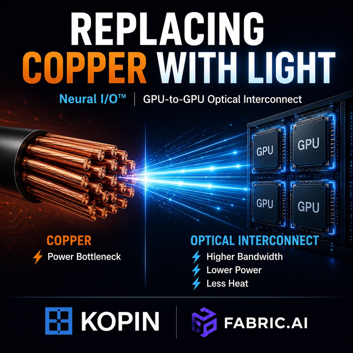
AI infrastructure is running into two major constraints:
Power. Bandwidth.
Neural I/O™ is targeting both through MicroLED-based optical interconnect technology designed for GPU-to-GPU communication.
If successful, it could expand $KOPN far beyond defense optics and FPV systems.
Early days. Massive opportunity.
$KOPN #AI #OpticalInterconnect #NeuralIO $FABC
3
19
45
1,985

May 26
Huawei’s “Tao / τ Law”: Tech Paper, White Paper, or Strategic Manifesto? 🧠🚀
🌟Insights from Zhihu contributor 无我梦中
Huawei’s new paper, “A Time Scaling Theory for Multi-Layer Electronic Systems” by Tingbo He, is better read as a semi-technical white paper strategic declaration, not as a pure theoretical research paper.
The core idea is powerful:
Replace “transistor size in nm” with “time constant τ” as the unified progress metric for semiconductors.
In plain English:
The future of chips is not only about making transistors smaller. It is about making the whole system wait less.
📌 What the Paper Is Really Saying
The paper’s logic can be summarized like this:
1️⃣ Moore’s Law was never just about space.
Smaller transistors mattered because they reduced time: faster switching, shorter wires, fewer boundaries, lower system delay.
2️⃣ After 7nm, geometric scaling gets weaker.
Intrinsic device delay no longer improves as easily. Local interconnect RC delay becomes more important. EUV depreciation, mask cost, verification, and design cost rise sharply. The cost-per-transistor curve is flattening or even turning upward.
3️⃣ So the industry should scale time directly.
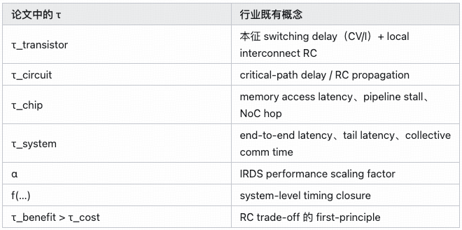
Huawei defines τ across 12 orders of magnitude — from transistor picoseconds to data-center seconds — as a shared optimization target.
4️⃣ Huawei gives three major proof points:
• LogicFolding on Kirin 2026: 55% density, 41% energy efficiency, 13% frequency at the same node
• Unified Bus for AI data centers: remote access latency from tens of μs to ~100 ns
• Hi-ONE optical I/O 3D Folding: solve the 2.5D packaging “N² vs N” bottleneck
5️⃣ Long-term roadmap:
• by 2031: “equivalent 1.4nm” density, 400 MTr/mm²
• by 2035: 100× AI hardware integration
The direction is meaningful. But the details need careful reading.
1️⃣ The End of the Geometric Era
The paper starts with a familiar claim: geometric scaling is reaching its limit.
This is mostly true.
Cost-per-transistor no longer reliably falls. EUV depreciation eats a large share of wafer cost. High-end chip design budgets can approach or exceed $1B. IRDS, Hennessy & Patterson, and Horowitz have all made similar arguments.
For a company like Huawei, restricted by advanced lithography access, this wall arrives earlier and hits harder.
But here the paper mixes two things:
• the global slowdown of Moore-style economics
• Huawei’s own manufacturing constraints
TSMC N3/N2, Intel 18A, and Samsung GAA are still improving transistor density. The physical path is not fully broken. What is broken is the old economic contract: new node = better cheaper.
So the paper’s framing is selective.
It uses an industry consensus to make Huawei’s own solution look like the inevitable path forward.
That is understandable as strategy. But as pure industry analysis, it goes a bit too far.
2️⃣ Time, Not Space ⏱️
This is the most philosophical part of the paper.
Huawei argues that Moore’s Law benefited users not because chips became “smaller,” but because systems became faster.
So metrics like:
• frequency
• latency
• bandwidth
• throughput
are all treated as different expressions of τ at different layers.
This framing is useful. It gives process, circuit, architecture, system, and software teams a shared language.
But academically, it is not completely new.
Hennessy & Patterson’s “A New Golden Age for Computer Architecture,” Horowitz’s energy-per-operation work, and IRDS “More than Moore” roadmaps have all pushed the same direction: transistor shrinking alone is not enough; system-level optimization matters.
So τ scaling is more like a new name for an old system-level idea, not a new physical discovery.
There is also some looseness in the math.
Bandwidth is not a time constant. It is bits per time. Throughput is not simply 1/τ either; it should be closer to:
throughput = 1 / τ_per_op × parallelism
Parallelism gets quietly absorbed.
For management narrative, that simplification is fine.
For a paper claiming a Dennard-level full-stack target, it feels light.
The real value of this section is not theory. It is language. It gives the whole industry stack one number to talk about: time.
3️⃣ LogicFolding: The Most Concrete Part 🏗️
This is the section most likely to go viral.
Huawei uses Kirin 2026 as proof that LogicFolding can deliver big gains without changing the process node:
• transistor density: 155 → 238 MTr/mm²
• performance-core energy efficiency: 41%
• peak frequency: 13%
• SRAM frequency: 40%
• clock buffers: -50%
• clock skew: -25%
• wire length: -30%
On paper, this looks almost like gaining a full process generation.
The engineering details are also specific:
• hybrid bonding pitch: 1.5 μm
• overlay: under 0.5 μm
• TSV CD / KOZ: under 1.5 μm
• TSV pitch: under 6 μm
• failure rate: under 100 ppm
• with repair, yield close to 100%
None of these numbers are impossible. But each sits close to today’s hybrid-bonding limits.
The bigger issue is methodology.
The paper does not provide:
• die photos
• SEM images
• wafer-level yield curves
• clear PPA baselines
• workload details for energy efficiency
• test corner / voltage / temperature conditions
So the headline numbers are attractive, but hard to independently verify.
There is also an important density caveat.
The formula counts both active tiers into one footprint. So 238 MTr/mm² is package-footprint density, not true silicon-area density.
That is normal in 3D integration. It is not deception. But readers must understand what “density” means here.
It measures how efficiently packaging uses 3D space, not how small the transistor is.
What is LogicFolding really?
It is not just process innovation.
It is not just packaging innovation.
It is not a brand-new theory either.
It is a combined design methodology:
sub-2 μm hybrid bonding cross-die logic partitioning custom EDA flow
The direction is physically sound: shorten critical interconnects, improve density, frequency, and efficiency.
But before third-party measurement appears, it is safer to discount the exact numbers.
Believe Huawei probably built something real.
Do not treat every number like audited silicon data yet.
4️⃣ AI Data Centers: Unified Bus, Hi-ONE, 3D Folding 🌐
The paper then moves from one chip to AI clusters.
Unified Bus
Unified Bus tries to collapse today’s complex data-center communication stack.
Traditional AI clusters rely on layers like:
• PCIe
• NVLink or private fabrics
• Ethernet / InfiniBand
• RDMA software stack
• DMA buffers and handshakes
Every layer adds latency and copying.
Huawei’s Unified Bus wants to expose memory semantics across chassis, with hardware-managed consistency. The paper claims remote access latency improves from tens of microseconds to about 100 ns, or roughly 500× τ reduction.
This number needs caution.
“Tens of μs” sounds like a TCP/IP baseline. But modern AI clusters using RoCEv2 or InfiniBand already reach the 1–3 μs range across racks, and NVLink can go below 1 μs inside a rack.
So the chosen baseline is favorable.
The “~100 ns” claim is also unclear.
If it refers to on-package or rack-local fabric protocol latency, it may be reasonable. But if it refers to cross-rack physical distance, it violates basic propagation delay. Light in fiber needs about 500 ns one-way for 100 meters.
So the most reasonable reading is:
100 ns refers to rack-local fabric/protocol latency, not full cross-rack physical latency.
The paper does not clarify this enough.
Hi-ONE Optical I/O
Hi-ONE is Huawei’s near-package optical engine.
The paper mentions:
• 8 Tb/s per module
• electrical SerDes distance reduced from 100 cm to 5 cm
• optical path extended from under 1 m to 100 m
Technically, this direction is credible.
Broadcom CPO, TSMC COUPE, Ayar Labs, Lightmatter, and others are all moving in the 4–8 Tb/s range around this timeline.
Huawei’s choice of near-package optics is also practical. It is less aggressive than full co-packaged optics, but likely easier to engineer.
The missing pieces are key parameters:
• BER target
• pJ/bit
• thermal reliability
• laser MTBF
• single-mode vs multi-mode fiber
• cost structure
So the direction is industry-aligned. It is not obviously behind, but not clearly ahead either.
3D Folding and the N² vs N Problem
This is one of the strongest arguments in the paper.
In a traditional 2.5D AI chip:
• logic die sits in the center
• HBM, SerDes, and power delivery enter from the edge
If die side length is N:
Compute ∝ N²
because compute grows with area.
But:
Bandwidth / I/O / Power ∝ N
because they enter from the perimeter.
That creates a topology deficit. Compute grows faster than the ability to feed it.
This is not a Huawei-only observation. NVIDIA Blackwell, Marvell, TSMC, Apple, and others are all dealing with the same bottleneck. But Huawei explains it very clearly.
The 3D Folding solution is natural:
Move constrained resources from the edge to the surface:
• backside power
• integrated voltage regulation
• hybrid-bonded memory
• near-package optical I/O
• 3D stacking
Then bandwidth, I/O, and power can scale more like area.
I fully agree with the direction.
But the paper underplays the cost.
Stacking active tiers creates hard problems:
• lower-tier heat removal
• bond yield × known-good-die yield × bond yield
• hard post-bond fault diagnosis
• limited repairability
• hybrid bonding equipment cost
• CTE mismatch reliability
• TSV stress affecting channels
The paper lists these challenges later, but treats them optimistically. Thermal, yield, and test remain the hardest parts.
5️⃣ Logic and Memory Re-Fusion 🧠
This section is more industrial than academic.
For decades, logic and memory were deliberately separated. CPU focused on compute. DRAM focused on storage. Standard buses connected the two.
That worked well in the PC era.
But AI changes everything.
Model parameters, KV Cache, activations, and gradients make data movement as important as compute. HBM, hybrid bonding, 3D SRAM, near-memory compute, and in-memory compute all point to the same trend:
logic and memory must get closer again.
This is not new. AMD 3D V-Cache is already in production. HBM4 is coming. CXL explores memory pooling. Samsung, SK Hynix, Sony, and others are all moving in related directions.
The paper does not add much academic novelty here.
But the strategic message is strong.
When the paper says long-term success belongs to those who can fuse logic and memory technologically and economically, it is effectively calling upstream partners:
• CXMT
• YMTC
• Hua Hong
• SMIC
• Huawei’s own packaging ecosystem
The message is:
AI hardware winners must integrate logic, memory, packaging, and economics together. No one can optimize alone anymore.
6️⃣ Open Challenges: The Best Section ⚠️
This is the most credible part of the paper because it openly admits what is not solved.
EDA is the first bottleneck
Current EDA tools optimize area, timing, and power mostly in 2D.
LogicFolding needs tools that treat stacked dies as one continuous 3D design object:
• cell-level cross-die partitioning
• 3D placement
• cross-die timing closure
• vertical interconnect parasitics
• KOZ modeling
• wafer-to-wafer process variation
Traditional 2D EDA cannot handle this well.
The paper says Huawei has preliminary internal tools, but also clearly implies:
τ-native EDA may be the single most important investment of the next decade.
Cross-wafer variation is hard
LogicFolding may bond wafers from different lots or nodes. Vth, drive current, and interconnect RC can vary more between wafers than inside one die.
Clock distribution and hold margins are hit first.
Adaptive compensation and τ-aware signoff may help, but this is engineering, not theory.
Vertical interconnect has its own τ cost
Every hybrid bond and TSV has R and C. TSV KOZ also pushes standard cells away.
So folding cannot be blind.
It must satisfy:
τ_benefit > τ_cost
This is a healthy self-constraint. The paper admits the threshold depends on workload and bonding pitch.
Energy is separate
τ is a time law, not a joule law.
If a super-node runs 10× faster but also consumes 10× power, τ scaling itself does not object — but the power grid will.
So τ optimization must be paired with:
• memory-semantic fabrics
• CPO / NPO
• backside power
• near-memory compute
• data-center DVFS
The paper also makes a useful point: τ headroom can be traded back into energy savings, just like smartphones used performance headroom to improve battery life.
Benchmarks must change
Linpack, MLPerf, and SPEC come from a world of single scalar scores.
τ scaling needs a τ-profile: a vector showing dominant τ and remaining headroom at each layer.
This is a good idea, but benchmark standardization requires industry cooperation. One company cannot do it alone.
The irony is clear:
The paper is honest in Section 6.
But this honesty also weakens the certainty of earlier claims.
If EDA, cross-wafer variation, energy, and benchmark standards are not mature yet, then numbers like 41%, 500×, 100×, and 1.4nm equivalent should be read with caution.
7️⃣ Roadmap and Future Claims 🗺️
This section is clearly a roadmap, not a research conclusion.
It projects:
• density from 155 MTr/mm² to 400 MTr/mm² by 2031
• Kirin performance-core frequency to 4 GHz by 2029
• AI hardware integration up 100× by 2035
• “the next dollar should follow τ, not nodes”
The message is strong. But the evidence varies.
The frequency table is eye-catching:
• Kirin 9000s: 2.6 GHz
• Kirin 9020: 2.65 GHz
• Kirin 9030 Pro: 2.75 GHz
• Kirin 2026 with LogicFolding: 3.1 GHz
• 2028: 3.71 GHz
• 2029: 4.0 GHz
But later rows are marked Pre-silicon, likely from STA simulation and experience-based extrapolation, not measured silicon.
Putting pre-silicon estimates next to mass-product data is common in corporate roadmaps, but academically it is weak.
The “2031 equivalent 1.4nm” phrase is also easy to misread.
It means density equivalent by package footprint, not true process-node equivalence.
It does not mean:
• equal frequency
• equal energy efficiency
• equal cost
• Huawei catches TSMC N1.4 in all dimensions
Media translating it as “Huawei catches TSMC by 2031” would be wrong.
The “100× by 2035” claim is the loosest. The baseline and unit are unclear: bandwidth? transistors? FLOPS? HBM capacity? rack-scale compute?
Without a clear unit, it is vision language, not engineering data.
The most important sentence is:
“The next dollar should follow τ, not nodes.”
This is not a technical proof. It is positioning for investors, regulators, and supply-chain partners.
It says: advanced packaging, memory bandwidth, fabrics, and system design now deserve the strategic weight that advanced lithography once monopolized.
τ Scaling Itself: Useful, But Overpackaged
τ scaling does not introduce a new physical quantity.
Every item maps to existing concepts.
Its real value is the unified scale.
That is useful. It lets process, circuit, architecture, system, and software teams talk about one shared optimization target.
But it is not Dennard scaling.
Dennard gave a stronger quantitative framework. τ scaling is closer to a cross-layer engineering KPI.
Useful? Yes.
A new law of physics? No.
Final Assessment 🧾
As an academic paper, it is not top-tier.
τ lacks a strict mathematical definition. The function:
τ = f(τ_transistor, τ_circuit, τ_chip, τ_system)
is more diagram than formula. The paper does not define whether f is additive, max-based, path-based, or something else.
The generational formula:
τᵢ₊₁ = τᵢ / α
looks like Dennard scaling, but α is empirical, not derived from physics.
Key numbers also lack methodology:
• 55% density
• 41% energy efficiency
• 13% frequency
• 500× τ reduction
• 100× integration
There is no die photo, SEM, third-party test, or full baseline.
As a research-track paper at ISCA or ISSCC, it would likely struggle. As an IEEE Micro perspective or CACM-style viewpoint, it makes more sense.
As an engineering roadmap, it is much stronger.
LogicFolding gives concrete parameters. The N² vs N packaging argument is clean and powerful. Section 6 is unusually honest about EDA, variation, vertical interconnect cost, energy, and benchmarks.
As an industrial strategy paper, it is excellent.
It connects process, packaging, interconnect, AI, and SoC into one story. It speaks to supply chains, capital markets, regulators, and partners at the same time.
Its message is clear:
Huawei’s next decade is not only about catching up on nodes. It is about building a full-stack system path around τ.
As an external communication text, it is almost perfect.
“τ, not nm” is a slogan that can last ten years.
“1.4nm equivalent” is a media hook.
“100× by 2035” creates imagination space.
LogicFolding, Unified Bus, and Hi-ONE are product names that can each become a story.
The biggest value of this paper is that it puts:
advanced packaging design methodology optical interconnect system fabric
into one unified framework, and gives China’s semiconductor industry a public methodology for moving forward even under EUV constraints.
The biggest weakness is overpackaging.
τ scaling is not mathematically as strong as Dennard scaling, but the paper places it in that role. The “100 ns remote access” claim is ambiguous. Key numbers are not third-party verified. Pre-silicon estimates enter the conclusion. “1.4nm equivalent” is easy to misinterpret if the equivalence dimension is not clarified.
So the right reading is:
not a pure theory paper, not just marketing, but a strategic engineering manifesto with real technical direction and unverified headline numbers.
It is worth taking seriously.
But not worth reading like a final verdict.
🔗 read more: zhihu.com/question/204217604…
#Huawei #Semiconductor #ChipDesign #AdvancedPackaging #EDA #AIInfrastructure #OpticalInterconnect #ChinaTech #TechLiberty
1
4
21
5,538

May 22
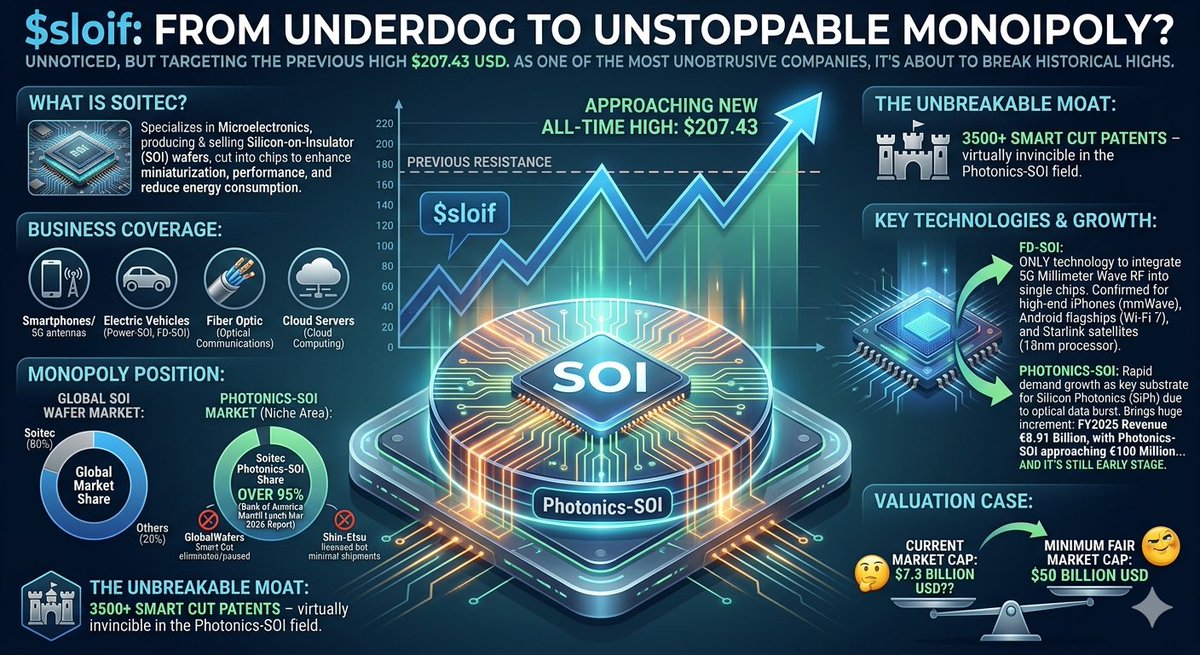
貌似在大家没注意的时候, $sloif也悄悄靠近了前高 $207.43 美金,作为当时最不起眼的公司,现在又要突破历史新高了:
或许你们都忘了 $sloif是一家什么公司:
1. Soitec是一家专注于微电子领域,主要生产和销售绝缘体上硅(SOI)晶圆,其产品被切割成芯片用于制造电子元件,目标是实现芯片小型化、提升性能、降低能耗。
他的业务也覆盖很多方面:
1. 他们可以给智能手机前端什么做模块和5G基础设施
2. 汽车方面他们有Power-SOI、FD-SOI,可以用来做电动车和自动驾驶雷达
3. 光通信方面他们则可以将光子器件集成在SOI基板上,以此来增加光通信能力。
4. 他们也做云计算
但我最看好的是他们是唯一获得主要硅光子晶圆厂认证的光子级SOI量产供应商。
这意味着什么?你要知道全球SOI晶圆市场只有10-12家主要玩家,然后Soitec一家就占了全球约80%的SOI晶圆供应量。
这已经趋向于垄断了……
而接下来可能会震惊你,在光子SOI这个细分领域里,美银美林2026年3月的光互联报告里表示Soitec在Photonics-SOI领域的市占率超过95%。
他的竞争对手GlobalWafers的Smart Cut则直接被淘汰暂停,而信越化学有授权但几乎没有实质性出货量。
他的护城河很自然的就是他那3500 项Smart Cut专利,在Photonics-SOI领域他几乎是无敌手。
另外他的FD-SOI是唯一能将5G毫米波射频集成进单芯片的晶圆技术,已确认用于高端iPhone(毫米波)、Android旗舰(Wi-Fi 7)以及Starlink卫星(18nm处理器)。
并且在光学爆发的情况下他的Photonics-SOI作为硅光子(SiPh)的关键基材需求快速增长,这给他们公司带来了巨大增量,单FY2025财年营收就达到8.91亿欧元,其中Photonics-SOI接近1亿欧元规模,而我们要注意的是现在还处于早期阶段………
所以,一个有着难以跨越的护城河,并且在光子SOI领域有着垄断地位的公司你告诉我只值73亿美金市值?
如果我们做一个简单的对比:
我们就拿同为半导体关键材料垄断供应商的 $ENTG , 他们的TTM营收约32亿美元,当前市值约220亿美元,对应PS约6.9x。
但问题来了Entegris是卖耗材的,可替换性远高于Soitec,而Soitec在Photonics-SOI领域市占率超95% 三大晶圆厂唯一认证供应商,这个溢价我认为还没被充分定价,并且客户认证壁垒几乎无法复制。
如果CPO/1.6T放量推动这块到5亿欧元,整体营收重回增长,PS扩张 收入增长双击,这些都实现的话……
我认为最少都是500亿美金的市值………
#SiliconPhotonics #CPO #AIDataCenter #Semiconductor #Photonics #SOIWafer #SmartCut #AIInfrastructure #OpticalInterconnect #1point6T
May 16

这周也算完满结束了,这周我关注的股票表现如何: 数据来自 Futubull
1. $AXTI
2. $sloif
3. $lite
4. $COHR
5. $aaoi
6. $sivef
7. $towa
8. $INDO
9. $DDOG
10. $RDDT
11. $RKLB
首先, $AXTI 这周涨幅度6.38%,稳健上升中,今天上涨7.65%回收了前俩日的部分跌幅。 公司本身于5月14日股东大会因法定人数不足休会,延至6月4日,这可能也有一定影响。
$AXTI 的上涨源自于背后强劲的Q1, 当然也不能缺少Wedbush,Northland和B. Riley等机构上调目标价的影响。
中美会谈中未提及磷化铟(InP)基板的出口管制, 这导致磷化铟出口许可证管控维持不变。
第二, $sloif本周下跌 15.15%, 他的下跌属于上周上涨34.25%的获利回吐 这周光学回调。
本周并无特大新闻出现。各位一个关注5.27号的全年财报。
第三, $lite这周涨幅达到 7.4%,最高触及1085.68美金。
$lite 本周能一度突破 $1000 美金源自于被纳入Nasdaq-100指数,生效时间为5月18日,资金在生效时间开启前提前入场。
另外, 一位Lumentum董事在5月12日进行了大额内部增持交易,市场认为这是公司管理层对于公司的高度自信的行为。
第四, $cohr本周涨幅高达14.08%, 属于关注公司中涨幅最高之一了。
本周5月13号,BofA证券将COHR目标价从365美元上调至400美元,维持中性评级,原因是因为他们看好800G和1.6T高速光学产品出货量持续增长。 这也能视为光学行业的加速发展。
另外,公司董事会内部在5.11和5.12出售2千股,但对于市场影响有限。同时,Coherent高管是此次特朗普访华代表团成员之一。
$aaoi 这家在本周涨幅27.81%, 本身公司股票曾一度突破$230美金,但由于公司在5.14号与Raymond James和Needham公司签署股权分配协议,建立最高6亿美元的随时增发(ATM)计划,市场在当天下跌8.75%。 本人认为是公司为了高速扩展而必须要进行的步骤。
5.12号AAOI宣布与美国第五大有线运营商Mediacom合作。
$sivef这周上涨23.83%, 本周在5.13号提前发布25年修正后的全年财报,而其中芬兰地区的营收暴涨引起大家猜想“ $NOK 是不是其重要合作伙伴之一”。 股价涨超$6.75美金。
另外, $sivef 5月11号通过了临时股东大会的批准完成了股票定向增发,认购方包括DNB Disruptive Opportunities、DNB Nordic Small Cap、Storebrand Sverigefond、Hudson Bay Capital Management等机构投资者。
这一次增发对公司而言是为了完成纳斯达克上市的预备工作。另外,公司为了防止这一次增发影响各位恐慌:公司承诺在增发完成后180天内不再发行新股,CEO、CFO及董事会成员承诺90天内不减持。
其次,公司董事会缩减至5人,新加入俩位:
Joakim Nideborn — 提议担任副主席: HMS Networks的CFO兼副CEO,工业自动化和工业ICT背景
Helena Svancar — 新董事:前爱立信全球M&A负责人。更多的负责Nasdaq上市服务。
$towa表现很差,下跌23.7%。 下跌幅度如此巨大是因为财报太差了H1净销售额小幅增长1.7%至544亿日元,但营业利润大跌22.1%,最糟糕的是EPS仅26.20日元,而市场预期90.90日元,相差3倍。唯一的亮点是股息从¥20提升至¥24,这说明公司财务不吃紧,反而增加股息,看来公司对于未来的订单很有信心。
财报那么差也有原因: 客户消减投资 公司成本增加 大多数产能要到h2才能实现。
$INDO 本周上涨13.21%,公司本周新签一家大型科技公司合同,预计2026年带来约5100万美元收入,这带来巨大增量。
$DDOG 本周上涨3.91%,5月12日高盛上涨其目标价到139美金,同时Datadog宣布管理层将出席即将举行的三场投资者会议:摩根大通全球科技媒体通信会议、战略决策会议(SDC),以及美国银行全球科技会议。
$rddt 本周很稳定,上涨1.52%。本周遭Phillip Securities下调评级,理由担心他们ai规模化发展不稳定………我其实不太了解。
$RKLB 本周上涨18.3% ,美国太空军司令Saltzman将军亲赴Rocket Lab参观。 个人很看好。
11家公司2家下跌,我想说本周现在都比较不错吧! 恭喜大家! 期待下周表现。
$AXTI $AAOI $COHR $LITE $SIVEF $SLOIF $TOWA $INOD $DDOG $RDDT $RKLB #AI #Semiconductors #Photonics #OpticalNetworking #SpaceTech

1
4
23
14,011

[Part 1. Japan’s Photonics-Electronics Convergence Stack]
Why Japan is not merely building optical components, but trying to reorganize the infrastructure of data movement
The most expensive thing in a data center is not always the computation itself.
As AI systems scale, data has to move constantly — from memory to compute, chip to chip, server to server, rack to rack. This invisible movement consumes power, creates heat, adds latency, and limits real performance.This is where photonics-electronics convergence matters.
It is not about replacing electrons with light everywhere. Logic and most computation stay electronic. The real question is simpler: at what point does electrical interconnect become too expensive, and optical transmission become the cheaper system-level choice?
1. PETRA is a map, not proof of a master plan
Look at PETRA (Photonics Electronics Technology Research Association). Its members include AIO Core, OKI, Sumitomo Electric, NEC, Fujikura, Fujitsu, Furukawa Electric, Mitsubishi Electric, NTT, NTT Innovative Devices, and 1Finity Inc.
This list is not a national command center. It is an industrial map. It shows which players are gathering around the same problem — the rising cost of data movement.
It does not prove market dominance or unified execution. It only shows alignment across layers.
2. The governing variable is the break-even point
Photonics is often called faster or lower-power. Those statements are directionally true, but too broad.The real governing variable is not raw speed.
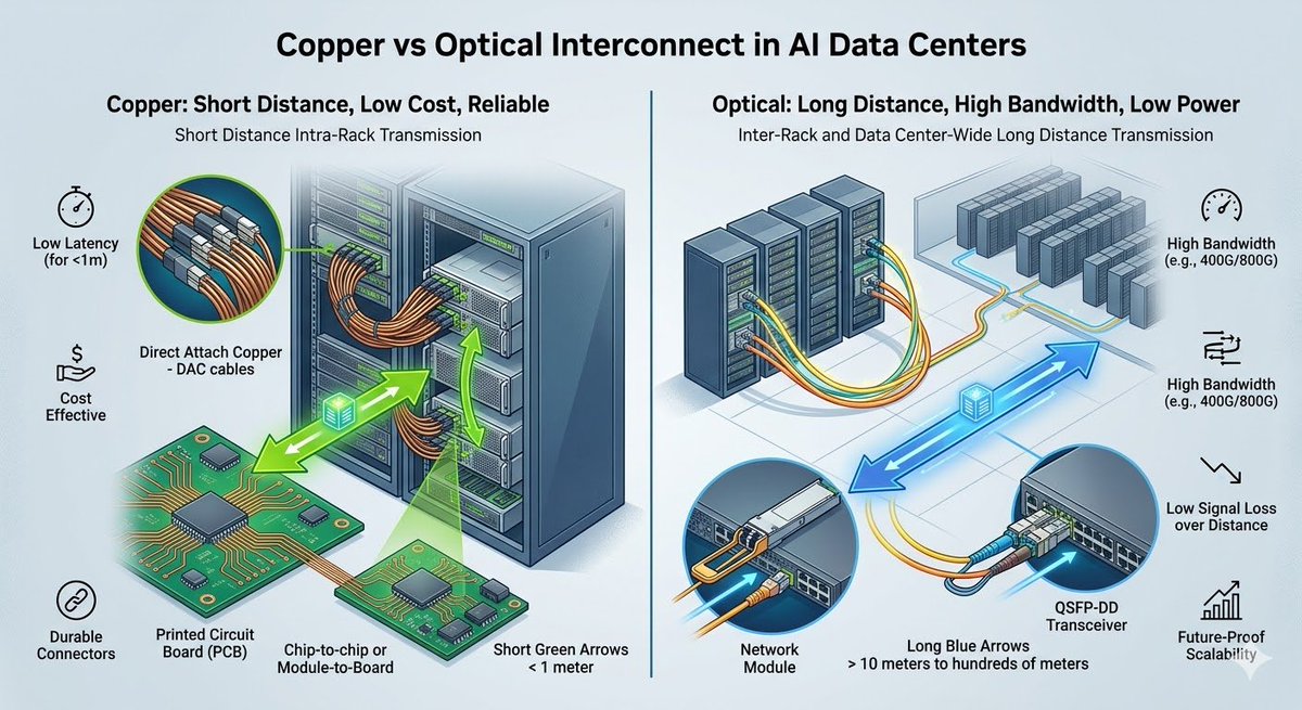
It is the economic break-even point where the total cost of scaling electrical interconnect (power, heat, retimers, board complexity) exceeds the overhead of optical conversion (laser, coupling loss, packaging, test).Electrical interconnect wins at short, simple distances.
Optics becomes compelling when distance and bandwidth make electrical scaling too expensive.This is a system-economics problem, not just an optical story.
#PhotonicsElectronics #IOWN #APN #SiliconPhotonics #JapanTech #DataCenter #CPO #OpticalInterconnect #AIInfrastructure

3
7
54
11,723

May 15
🏗️ AI Architect’s Daily Briefing: May 15, 2026
I see today’s news as the emergence of the "Silicon-to-Strategy" layer, where we finally reconcile hardware bottlenecks with global regulatory and economic frameworks.
1. Cisco Declares AI "Networking Supercycle" with Massive $9B Guidance Shift
Surging demand for hyperscaler infrastructure has pushed Cisco to lift its AI forecast by nearly 80%, signaling a fundamental re-architecture of the global data center backbone.
Architect's Take: We are moving from the "Compute Bottle" to the "Interconnect War", if your fabric isn't designed for the massive east-west traffic of distributed training, your GPU clusters are just expensive space heaters.
2. OpenAI Proposes US-Led Global AI Oversight Body Including China
The move toward an international regulatory framework aims to set safety benchmarks for frontier models, acknowledging that AI risk management requires a unified global security protocol.
Architect's Take: Governance is finally catching up to the API; we are transitioning from "Move Fast and Break Things" to a "Zero Trust" architectural mindset for foundational intelligence.
3. Korea’s KOSPI Breaches 8,000 Milestone on Semiconductor and AI Rally
Driven by high-bandwidth memory (HBM) demand and a tripling of national AI spending, the Seoul market’s historic run underscores AI as the primary driver of 21st-century equity.
Architect's Take: This is the capital markets pricing in the reality that silicon production capacity is now the ultimate proxy for national GDP.
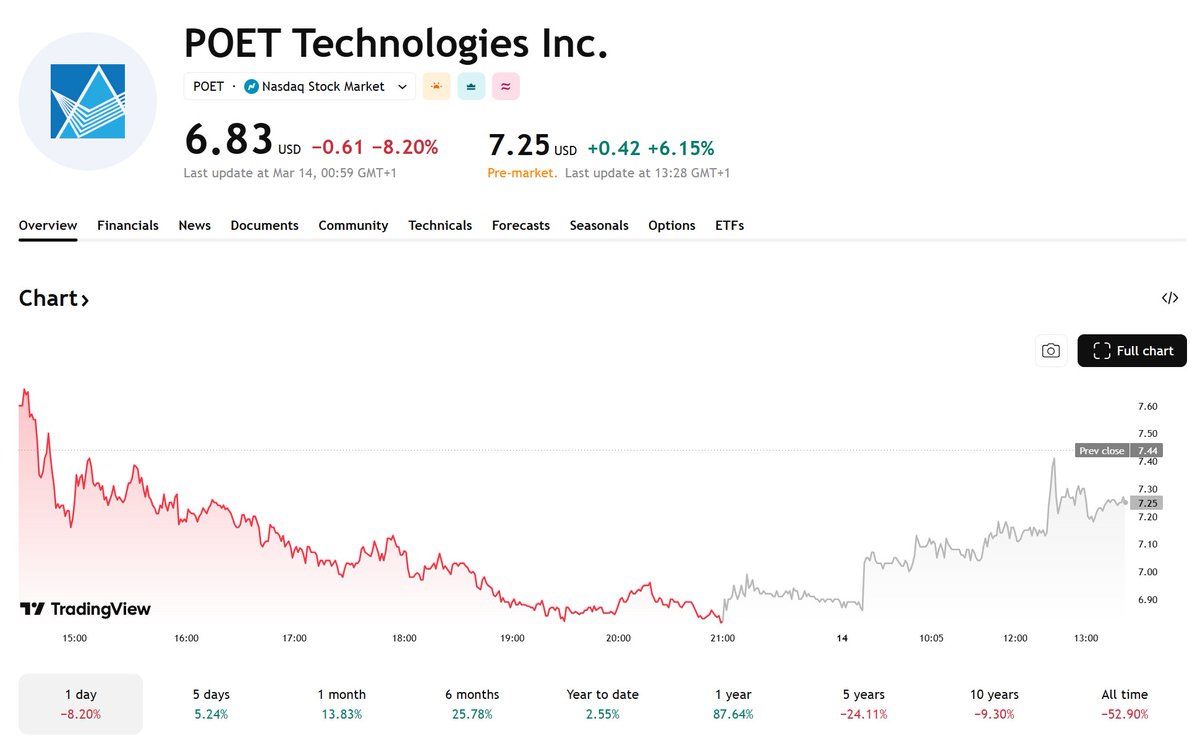
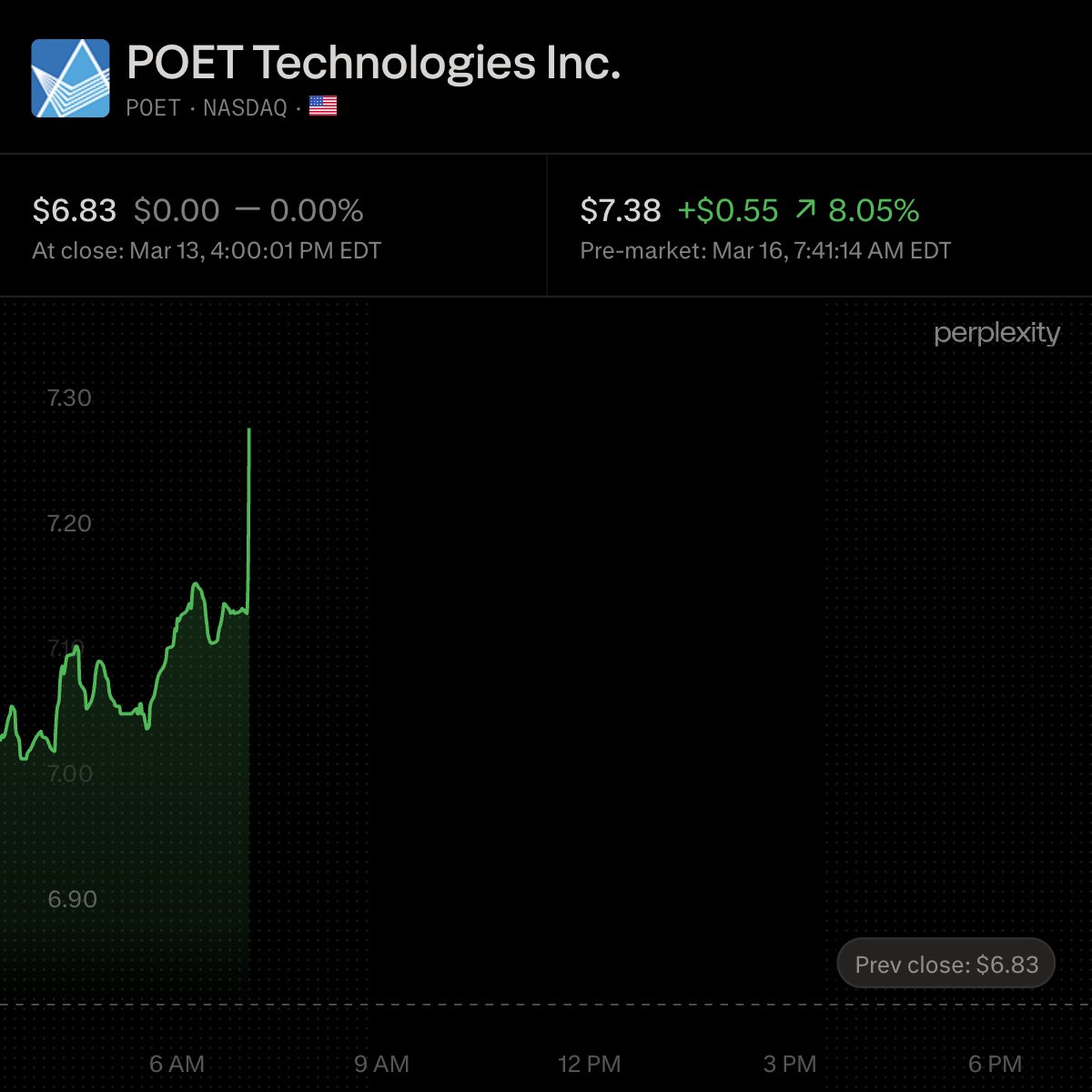
4. POET and Lumilens Unveil Electrical-Optical Interposer (EOI) for Next-Gen AI
This breakthrough in wafer-level photonic integration aims to eliminate the optical bottleneck, enabling higher density and bandwidth for frontier AI workloads.
Architect's Take: The laws of physics are the final frontier; shifting from electrons to photons at the interposer level is the only way we maintain the "Performance-per-Watt" curve required for AGI.
5. Apple Signals Massive Strategy Shift with "Extensions" for Third-Party AI
Reports indicate iOS 27 will allow users to swap Apple Intelligence for providers like Google or Anthropic, breaking the traditionally closed ecosystem for the first time.
Architect's Take: Modularity always wins in the long run, even for Apple, the "Single Vendor" approach can’t keep pace with the hyper-specialization occurring at the model layer.
#AIArchitecture #Infrastructure #Semiconductors #GlobalGovernance #OpticalInterconnect #AppleIntelligence #Cisco #Nvidia #SystemsDesign #TechStrategy

58

May 14
L’AI sta iniziando a scontrarsi con un limite fisico che pochi fuori dal settore vedono:
non i GPU, non i transistor, ma le interconnessioni.
Ogni nuovo cluster AI aumenta enormemente traffico dati, latenza, consumo energetico e complessità del networking. Ed è qui che Marvell sta spingendo sulla photonic fabric.
L’idea è semplice ma enorme: usare connessioni ottiche integrate vicino al package per spostare dati tra rack AI con molta meno energia rispetto al rame tradizionale.
Questo comporta, meno perdita, meno calore, più distanza, più scala.
Il dato interessante non è il marketing “4x efficiency”, é il fatto che il settore sta iniziando a trattare il networking come un collo di bottiglia energetico, non solo computazionale.
Per anni il focus era “più FLOPS”, ora il problema è: come muovi petabyte tra acceleratori senza trasformare il datacenter in un reattore termico?
La fotonica integrata potrebbe diventare una delle tecnologie chiave della prossima generazione AI infrastructure.
Perché il futuro dell’AI non dipende solo da quanto calcolo generi, dipende da quanto efficientemente riesci a collegarlo.
#Semiconductors #Photonics #AIInfrastructure #Datacenter #Marvell #OpticalInterconnect #AIChips
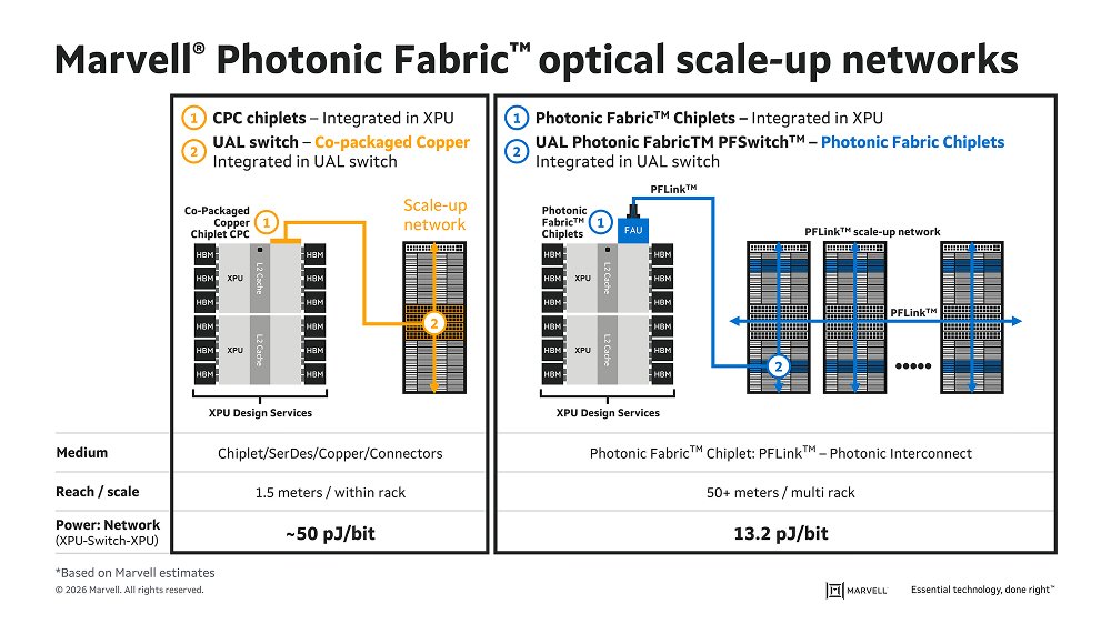
May 14

Marvell Photonic Fabric: 4x better energy efficiency, lower latency, and multi-rack reach.
2
38

May 13
🔥 $POET x Lessengers (Korean startup)
• POET invested $3M as strategic partner
• Joint 1.6T optical module — sample by H1 2026
• 2 major North American companies in talks
• LG Group, SK, Furiosa AI partnerships confirmed
#POET #Lessengers #OpticalInterconnect #1point6T
3
1
4
552

May 12
$KOPN is targeting the next one.
GPU-to-GPU communication.
What makes it different from other optical?
Others: one-directional / serial
Kopin NeuralI/O™: Bi-directional Parallel
GPUs talk AND listen at the same time.
The entire data center operates like a single brain. 🧠
✅ Copper wiring → MicroLED optical replacement
✅ Bi-directional parallel transmission → bandwidth explosion
✅ Zero signal loss. Zero heat waste.
✅ Only U.S. manufacturer of 4 microdisplay types
✅ Exclusive collaboration with Fabric.AI
If NVIDIA revolutionized compute,
can Kopin revolutionize connection?
The next GPU moment
might not come from silicon.
It might come from light. 💡
Still early stage. But the architecture is right.
And the moat is being built quietly.
$NVDA $FABC $KOPN
#Kopin #MicroLED #OpticalInterconnect
2
104
May 7
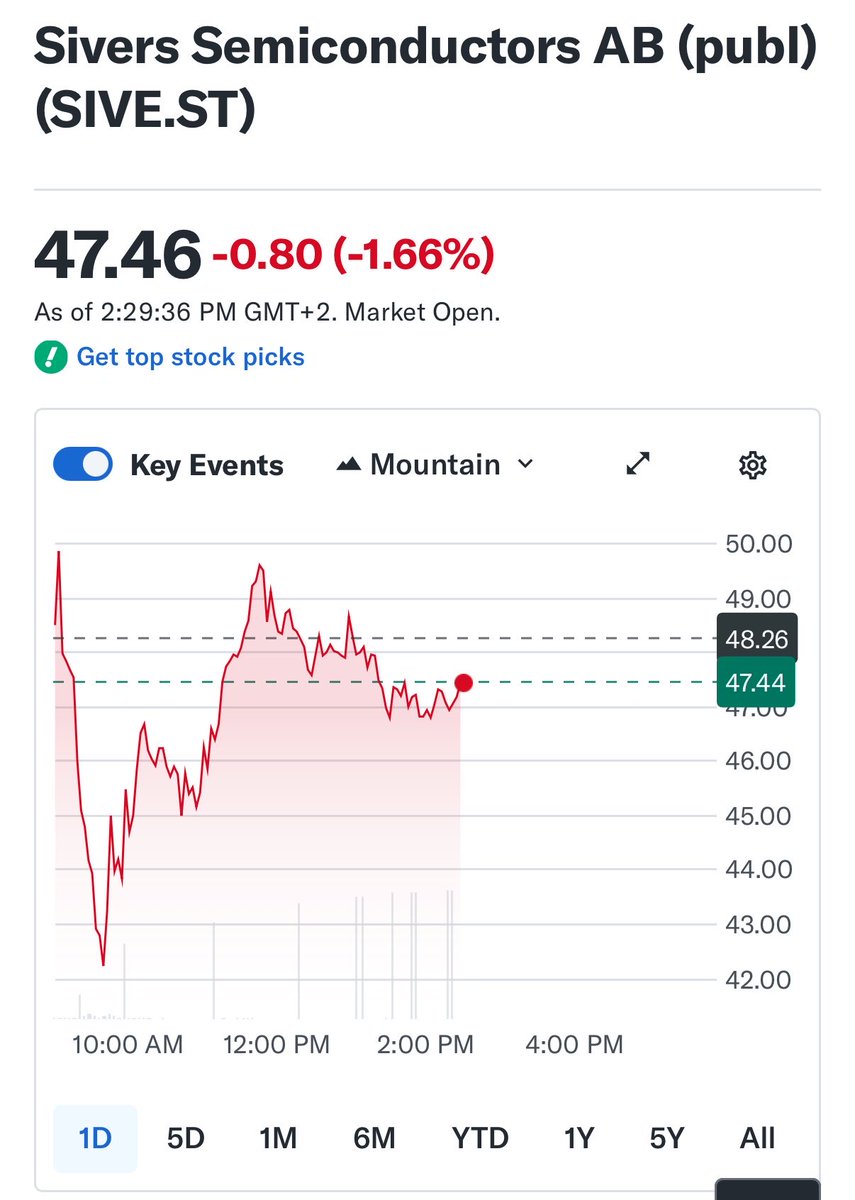
今天的剧情还是太熟悉了,瑞典从早上就开始砸盘到下跌10%,现在接近美股开盘 $sive 只下跌了2%。 看来他们也清楚地知道不论他们卖的有多严重,美国人都会买起来。
为了新粉丝们知道 $sive 这一家公司有多大的潜力,我和各位简单的总结一下:
首先公司在光子和无线领域有着接近60年的研究,然后公司通过两大业务板块运营——无线(Wireless)和光子(Photonics),开发、制造并销售芯片、组件、模块和子系统,面向北美、欧洲和亚洲市场。
🤝 已确认合作(现有)
📡 光子 / AI 数据中心方向
Ayar Labs(美国):
Sivers 的激光阵列集成于 Ayar Labs 的 SuperNova™ 多波长光源,支持 4 Tbps 数据通信。 2024年12月,双方扩展合作至高容量光学I/O的量产认证阶段,商业量产预计在2026年中至2027年底启动。 Ayar Labs 的生态圈里还有 NVIDIA、HPE、Intel、GlobalFoundries、Alchip、TSMC 作为战略伙伴。
Jabil(捷普,美国):
Jabil 计划基于 Sivers 的 DFB 激光器开发 1.6Tbps 线性接收光收发器模块,专为 AI 数据中心设计。
POET Technologies(加拿大):
双方合作将 POET 的光学中介层平台与 Sivers 的激光器结合,开发用于插拔式收发器和 CPO 架构的光引擎,原型机预计2026年上半年向客户展示,量产目标为2026年底。
O-Net Technologies Enablence Technologies(三方合作):
O-Net 作为 ODM 合作方,将 Sivers 激光阵列与 Enablence 的 NxN 星型耦合器整合,打造面向 AI 数据中心和 HPC 的外部光源(ELS)模块。
WIN Semiconductor(台湾,代工):
Sivers 与台湾晶圆代工巨头 WIN Semiconductor 建立战略合作,用于 DFB 激光器的大规模量产,构建光子业务的无晶圆厂生产模式。
LioniX International Chilas B.V.(荷兰,三方合作):
三方合作开发窄线宽 CW 可调谐 1310nm 激光器,用于光通信和传感领域。
匿名战略客户(AI 激光阵列):
2024年签署 130万美元原型合同,预计量产后年芯片出货量超过数百万颗,2026年后持续放量。
匿名 LiDAR 客户:
该 LiDAR 客户计划于2026年第四季度启动 Sivers 激光器和放大器的量产,2026—2030年间预计累计贡献营收 2800万至5300万美元。
📶 无线 / 5G / 卫星通信方向
Tachyon Networks(美国,FWA):
Sivers 收到 Tachyon Networks 300万美元生产订单,用于加速下一代 28GHz 天线模块部署。 最新又签署150万美元协议,合作开发 60GHz 毫米波收发器,推进 28GHz 和 60GHz 统一平台。
Doosan(斗山,韩国):
150万美元战略合作协议,联合开发 Ka 波段 SATCOM 卫星天线面板。
欧洲空间局(ESA):
获得约90万美元、为期18个月的合同,开发下一代卫星通信波束成形集成电路(BFIC),支持欧盟 IRIS²卫星互联网计划。Sivers 是欧盟唯一商业毫米波 BFIC 提供商。
匿名欧洲卫星通信公司:
签署1640万美元战略开发协议,为客户当代及下一代地面终端提供多款芯片,长期合作预计延续至2030年以后。
美国国防承包商(匿名):
获得80万美元战略开发合同。
GlobalFoundries(代工,无线业务):
Sivers 无线业务的晶圆代工合作方,构建无晶圆厂量产模式。
DigiKey(美国,分销):
战略分销合作,通过全球最大电子元器件分销平台之一,向全球工程师和客户扩大毫米波产品及评估板的销售覆盖。
总的来说:Sivers 的合作网络覆盖三大赛道——AI 数据中心光互联(CPO)、5G/6G 毫米波无线、卫星通信,且通过 Ayar Labs 与硅谷顶级 AI 生态形成了间接但重要的战略联系。关键看点是 CPO 商业化节奏能否在 2026—2027 年兑现。
#AIDataCenter #CoPackagedOptics #CPO #PhotonicAI #AIInfrastructure #Photonics #DFBLaser #OpticalInterconnect #SIVE #SiversSemiconductors #SIVEST
11
27
160
21,577


Apr 28
💡 News Update | @Kopin Corporation (NASDAQ: $KOPN)
CEO Michael Murray joins us to discuss a major strategic collaboration and $15 million purchase order from Fabric Ai to develop MicroLED-based Optical Interconnect Technology — designed to replace traditional copper wiring between #GPUs and high-performance processors in #smartdatacentres.
▶️ Watch the full interview here ➝ youtu.be/4VP7yQbHETQ
#Kopin $KOPN #MicroLED #DataCentre #AIInfrastructure #OpticalInterconnect #Semiconductors #Tech #Defense
2
11
561

Apr 23
🚀 TPU v8 Catalyst Alert
Google’s new TPU v8 just supercharged optical interconnect demand (OCS Boardfly full-mesh).
Supply chain mapping:
$POET → Luxshare → Google TPU v8
Luxshare is ramping POET-powered 800G AI optical engines straight into Google’s massive inference clusters.
Photonics winning the AI arms race. $POET just got a major tailwind
#POET #AI #OpticalInterconnect
4
7
38
6,065

Really insightful and interesting article about the @SiversSemicond story! Highly recommended reading to understand the journey and valutation of a leading #semiconductor company in #Wireless #mmWave #SATCOMM and #Photonics #AI #OpticalInterconnect.
2
7
783

Mar 25
黄仁勋GTC 2026明确指出:AI工厂未来铜缆与光通信并存,而非光学完全取代铜!
👉3月初,NVIDIA豪掷40亿美元(各20亿)投资Lumentum和Coherent,并锁定多年大额采购承诺,加速CPO(共封装光学)和硅光子学研发,目标支持吉瓦级AI工厂的Scale-up/Scale-out乃至Scale-across。
👉铜缆在短距(机架内)仍具成本、可靠性和功耗优势;👉光学(CPO)则在长距、高带宽、低功耗上突破“铜墙”,1.6T激光 光引擎大幅提升能效。
黄仁勋强调:“我们需要更多铜容量,也需要更多光学容量。”双轨并行,英伟达提前锁住光互联供应链,为下一代AI基础设施铺路。
#NVIDIA #CPO #OpticalInterconnect #GTC2026
21
1
4
626

Mar 16
Scalable Photonics: $POET Technologies & LITEON Join Forces 2301.JP
The bottleneck for next-gen AI isn't just compute - it’s interconnects.
As data centers struggle with power density and latency, the industry is pivoting toward integrated photonics.
The newly announced partnership between POET Technologies and LITEON is a massive signal that this transition is hitting the "execution" phase.
➡️Why This Matters:
The collaboration bridges the gap between high-level innovation and mass-market availability:
➡️The Tech:
POET’s Optical Interposer™ platform eliminates costly active alignments and reduces component count, offering a "semiconductor-like" approach to assembly.
➡️The Scale:
LITEON brings world-class, high-volume manufacturing expertise. For AI hyperscalers, "cool tech" is useless without a reliable, high-yield supply chain.
➡️The Roadmap:
With prototypes expected by late 2026 and volume production in 2027, this timeline aligns perfectly with the rollout of next-gen 1.6T and 3.2T optical transceivers.
➡️The Bigger Picture
We are moving away from traditional "plugging in" optics toward CPO (Co-Packaged Optics) and highly integrated modules.
By combining POET’s hybrid integration with LITEON’s operational muscle, we are looking at a serious contender for the hardware backbone of the 2027 AI infrastructure.
➡️The verdict?
This partnership validates POET’s platform as a manufacturable reality, not just a lab success. Keep a close eye on their 800G and 1.6T milestones over the next 18 months.
#Photonics #AIInfrastructure #Semiconductors #OpticalInterconnect #POETTechnologies #LITEON #DataCenters #TechInnovation
Mar 16

$POET is partnering with LITEON to develop optical modules for AI and data center applications, combining POET’s optical interposer platform with LITEON’s manufacturing capabilities. The companies expect prototypes by late 2026 and volume production in 2027.
4
7
37
6,223

Mar 12
We’re excited to announce a long-term collaboration with Marvell to develop next-generation, high-density micro-LED connectivity solutions for AI infrastructure.
marvell.com/company/newsroom…
#AI #MicroLED #Datacenter #Semiconductors #OpticalInterconnect
3
905