
🚀 Success Doesn't Come From Motivation Alone
Many aspiring VLSI engineers wait for the perfect time to start learning.
The perfect course.
The perfect project.
The perfect opportunity.
The truth is:
Successful engineers start before they feel ready.
📌 You won't always feel motivated.
📌 You won't always feel confident.
📌 You won't know everything before your first interview.
What matters is showing up consistently.
Learning one concept.
Writing one module.
Solving one problem.
Preparing for one more interview.
Small efforts repeated over time create big results.
The engineers who succeed are not always the most talented.
They are often the ones who keep learning when others stop.
💡 Progress is better than procrastination.
💡 Consistency beats intensity.
💡 Every interview is a learning opportunity.
Keep learning.
Keep building.
Keep preparing.
Your next opportunity could be closer than you think.
#VLSIBeginners #InterviewsClub #InterviewPreparation #VLSI #Semiconductor #ASIC #RTLDesign #PhysicalDesign #STA #DFT #CareerGrowth

15
🚀 500 Followers. Thank You. @LinkedIn
A few months ago, VLSI Beginners was just an idea.
An idea to help aspiring VLSI engineers learn, prepare for interviews, connect with industry professionals, and build successful careers in the semiconductor industry.
Today, I am excited to share that our community has crossed **500 followers on LinkedIn.**
For large pages, 500 followers may seem like a small number.
For us, it represents something much bigger.
It represents 500 students, freshers, engineers, mentors, and professionals who believe in continuous learning and career growth.
It represents 500 people who have chosen to be part of this journey.
Over the last 30 days alone, more than **400 professionals joined our community**, which shows the growing interest in VLSI learning, interview preparation, and career guidance.
This milestone motivates us to keep building.
Our mission remains simple:
✅ Share valuable VLSI learning resources
✅ Help engineers prepare for interviews
✅ Connect learners with industry professionals
✅ Provide career guidance and mentorship
✅ Build a strong VLSI community
We are still at the beginning of our journey, and there is much more to come.
Thank you to every person who follows, engages with our content, shares feedback, and supports VLSI Beginners.
Your support means everything.
🎯 Next Milestone: 1,000 Followers
Let's continue learning, growing, and building together.
#VLSIBeginners #VLSI #Semiconductor #ASIC #FPGA #Verification #PhysicalDesign #DFT #STA #InterviewPreparation #CareerGrowth #ElectronicsEngineering

1
32
🚀 Just Released: 1500 General VLSI Interview Questions
After months of research and compilation, I've created a comprehensive VLSI Interview Question Bank designed for students, freshers, and experienced engineers preparing for semiconductor industry interviews.
📘 What's Included?
✅ VLSI Fundamentals
✅ Digital Electronics
✅ CMOS & Circuit Design
✅ RTL Design
✅ Verification
✅ STA
✅ Physical Design
✅ DFT
✅ FPGA
Plus:
🎯 280 Project-Based Interview Questions
🎯 275 Company-Specific Questions
(Intel, AMD, NVIDIA, Qualcomm, Broadcom, Synopsys, Cadence, Samsung, MediaTek, Texas Instruments)
🎯 200 Mock Interview Questions
🎯 200 Rapid Revision Questions
🎯 Last-Minute Revision Sheets
Total: **1505 Curated Questions & Revision Points**
Whether you're preparing for your first VLSI interview or planning a job switch, this question bank can help you identify knowledge gaps and strengthen your interview preparation.
I'd love to hear from the community:
👉 What was the toughest VLSI interview question you've ever been asked?
Comment below and let's help fellow engineers prepare better.
#VLSIBeginners #VLSI #ASIC #RTLDesign #Verification #STA #PhysicalDesign #DFT #FPGA #Semiconductor #InterviewPreparation #ElectronicsEngineering #ChipDesign

1
1
1
72

Jun 9
Seeking Physical Design roles M.Tech VLSI
Completed full ASIC flow on a 32nm RISC-V core and contributed to an SCL 180nm tapeout. Looking for PD/STA fresher or intern positions. Happy to share resume. Any referrals appreciated.
#VLSI #PhysicalDesign #ASIC
150

Jun 8
Mee network lo VLSI/ASIC/RTL Design/Verification/Physical Design related openings unte share cheyyandi. Referral or guidance unte chala help avuthundi.
RT/Repost chesi reach penchandi 🙏
#VLSI #ASIC #RTLDesign #Verification #PhysicalDesign #Semiconductor #OpenToWork #Freshers
204

Explore the fundamentals of standard cell architecture, layout considerations, and their role in modern IC design
Read more: signoffsemiconductors.com/la…
#VLSI #ASICDesign #PhysicalDesign #SignOffSemiconductor #ChipDesign
9
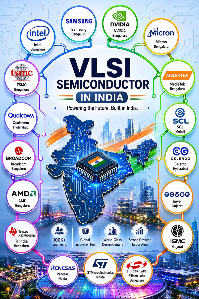
🇮🇳 VLSI Semiconductor Industry in India: A Growing Global Powerhouse
India is steadily strengthening its position in the global semiconductor ecosystem. Over the past decade, the country has become a preferred destination for semiconductor design, research, development, and innovation.
Today, many of the world's leading semiconductor companies have established design centers, engineering teams, and R&D facilities across cities such as Bengaluru, Hyderabad, Noida, Pune, Chennai, and Ahmedabad.
Some of the major players with a significant presence in India include:
🔹 Intel
🔹 Samsung Semiconductor
🔹 NVIDIA
🔹 Qualcomm
🔹 Broadcom
🔹 AMD
🔹 Texas Instruments
🔹 Micron
🔹 MediaTek
🔹 Synopsys
🔹 Cadence
🔹 ARM
🔹 STMicroelectronics
🔹 Renesas
🔹 Silicon Labs
🔹 Tower Semiconductor
🔹 SCL
🔹 ISMC and many others.
These companies are contributing to the development of advanced technologies used in:
✅ Artificial Intelligence (AI)
✅ High-Performance Computing (HPC)
✅ Automotive Electronics
✅ 5G & Wireless Communication
✅ Consumer Electronics
✅ Data Centers & Cloud Computing
✅ Internet of Things (IoT)
✅ Aerospace & Defense
India is home to thousands of semiconductor professionals working in areas such as:
• RTL Design
• ASIC Design
• Design Verification
• FPGA Development
• Physical Design
• DFT (Design for Test)
• Static Timing Analysis (STA)
• Analog & Mixed Signal Design
• Embedded Systems
• EDA Tool Development
With increasing government support, new semiconductor manufacturing initiatives, and growing investments from global technology companies, the demand for skilled VLSI engineers is expected to rise significantly in the coming years.
For engineering students, fresh graduates, and professionals looking to enter the semiconductor industry, this is one of the most exciting periods to build expertise in VLSI design and chip development.
🚀 The future of electronics, AI, automotive systems, communication networks, and computing will be powered by semiconductors—and India is becoming an important part of that future.
Which semiconductor company would you most like to work for?
👇 Share your answer in the comments.
#VLSI #Semiconductor #ChipDesign #ASIC #RTLDesign #Verification #PhysicalDesign #FPGA #SemiconductorIndustry #ElectronicsEngineering #VLSICareers #IndiaTech #VLSIBeginners
1
1
2
241

May 24
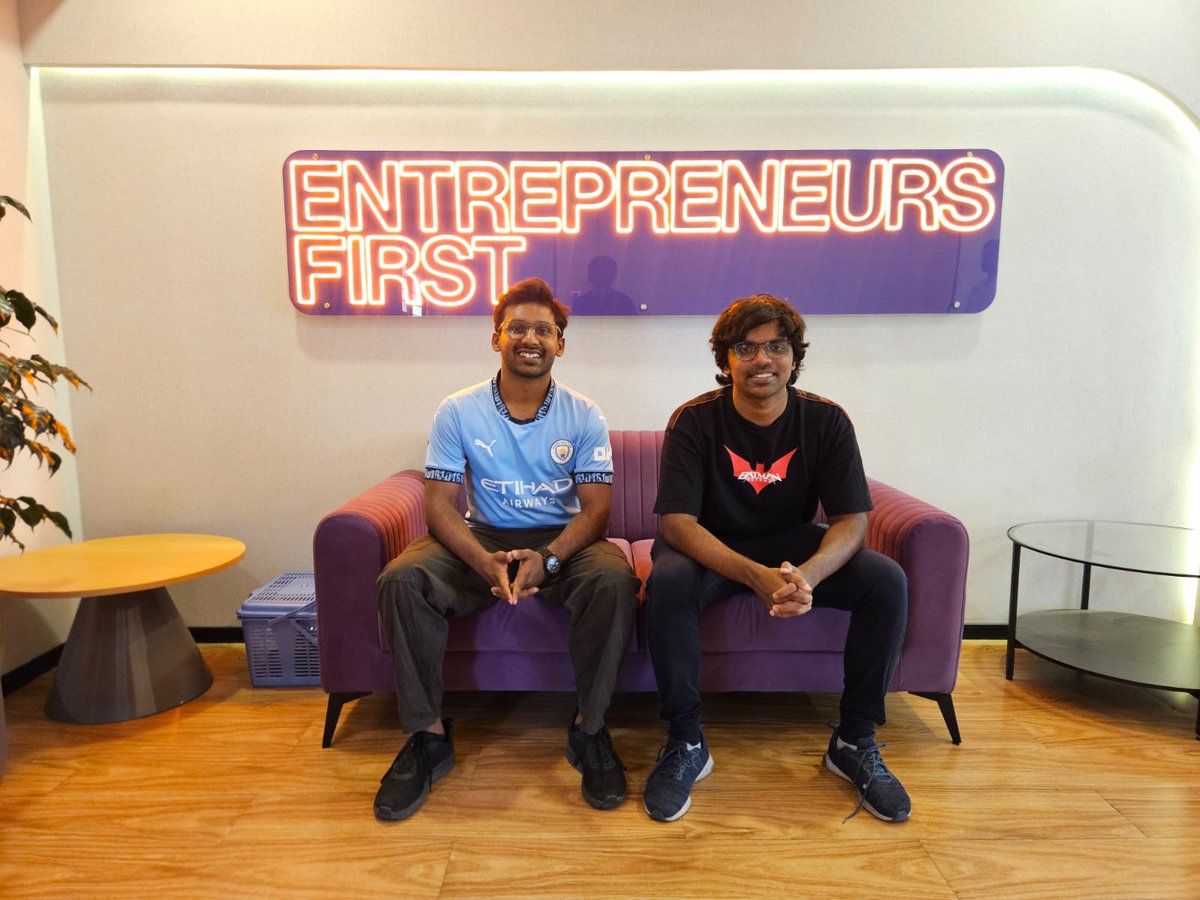
Really excited for this journey. Feels surreal that conversations we’ve been having for years are now turning into a company.
Thanks @join_ef , @suhasasumukh , @localhostIND for all the support !!
Time to build @archgen_
#semiconductors #EDA #physicaldesign #ASIC #chipdesign #AI #chips
May 24

Thrilled to announce that @naveen_venk and I have joined @join_ef to build @archgen_ .
Our thesis is simple:
The next generation of semiconductor design tools will not just automate workflows they will learn from every engineer who uses them.
Chip design today is full of repeated manual effort.
1. A senior physical design engineer fixes a timing issue.
2. Another engineer solves a congestion problem.
3. Someone else discovers a better macro placement strategy.
4. A team spends weeks tuning PPA across hundreds of experiments.
But most of this knowledge disappears into scripts, logs, webex threads, reports, and individual engineer's memory.
We’re changing that.
At @archgen_ , we’re building self-learning agents for semiconductor design, with specific focus on physical design.
Our agents work alongside engineers, run EDA flows, inspect reports, debug failures, optimize PPA, and capture the reasoning behind successful workflows.
1. When an engineer solves something, the agent learns.
2. When a strategy fails, the agent remembers why.
3. When a similar problem appears again, the agent can reuse the right approach.
Over time, this becomes an organisational memory layer for chip design. One that compounds.
Our vision is to make chip design feel less like manually stitching together fragmented tools and more like working with a team of expert agents that get better every day.
The future of semiconductor design is self-learning.
Huge thanks to @suhasasumukh 🐐 and @localhosthq for being extremely generous with their credits and supporting us throughout.
#semiconductors #EDA #physicaldesign #ASIC #chipdesign #AI
1
3
13
802

May 24
Thrilled to announce that @naveen_venk and I have joined @join_ef to build @archgen_ .
Our thesis is simple:
The next generation of semiconductor design tools will not just automate workflows they will learn from every engineer who uses them.
Chip design today is full of repeated manual effort.
1. A senior physical design engineer fixes a timing issue.
2. Another engineer solves a congestion problem.
3. Someone else discovers a better macro placement strategy.
4. A team spends weeks tuning PPA across hundreds of experiments.
But most of this knowledge disappears into scripts, logs, webex threads, reports, and individual engineer's memory.
We’re changing that.
At @archgen_ , we’re building self-learning agents for semiconductor design, with specific focus on physical design.
Our agents work alongside engineers, run EDA flows, inspect reports, debug failures, optimize PPA, and capture the reasoning behind successful workflows.
1. When an engineer solves something, the agent learns.
2. When a strategy fails, the agent remembers why.
3. When a similar problem appears again, the agent can reuse the right approach.
Over time, this becomes an organisational memory layer for chip design. One that compounds.
Our vision is to make chip design feel less like manually stitching together fragmented tools and more like working with a team of expert agents that get better every day.
The future of semiconductor design is self-learning.
Huge thanks to @suhasasumukh 🐐 and @localhosthq for being extremely generous with their credits and supporting us throughout.
#semiconductors #EDA #physicaldesign #ASIC #chipdesign #AI
23
15
76
6,588

4 Nov 2025
Even With AI Inroads, Human Chip Designers Still Essential semiengineering.com/even-wit…
#semiEDA #analog #verification #AI #workforce #chiparchitecture #physicaldesign #semiconductor

1
3
8
1,213

22 Sep 2025
It's about understanding how people seek, use, and understand information – whether that information is a digital file or the location of the sugar...
#InformationArchitecture #DesignThinking #UserExperience #PhysicalDesign #Innovation #UXDesign
lnkd.in/p/dP_D7nyW
1
20

28 Aug 2025
We’re Hiring – Physical Design Engineer
Looking for experienced professionals to join our VLSI team in Bangalore.
#WeAreHiring #PhysicalDesign #VLSIJobs #BangaloreJobs #HiringNow #ChipDesign #SemiconductorJobs #Innovus #FusionCompiler #ASICDesign #TechHiring #Speraspect

2
88

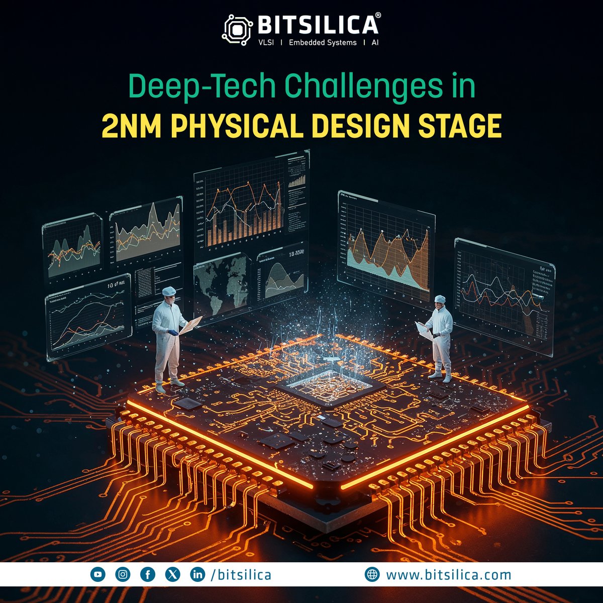
18 Jun 2025
Designing at 2nm isn't just hard—it's quantum.
Challenges:
• Quantum tunneling
• Advanced DRCs
• PPA balancing
• Tool complexity
See how deep tech teams are solving the unsolvable:
🔗 bitsilica.com/deep-tech-chal…
#2nm #Semiconductors #PhysicalDesign #EDA #ASIC #BITSILICA
2
33

28 Apr 2025
🚀 Hiring Physical Design Engineers!
📍 Bangalore/Hyderabad
✅ 4–15 yrs exp | AMD flow, PNR, STA
⏳ Notice: 0–30 days
📩 careers@smartsocs.com
#Hiring #PhysicalDesign #Jobs

2
125

10 Mar 2025
Speeding Up Physical Design Verification for AMS Designs semiwiki.com/eda/353813-spee… #Ams #CadenceVirtuoso #CalibrePatternMatching #CalibreRealtime #DesignSymmetry #PhysicalDesign
2
295

25 Feb 2025
🎉 WE HAVE A NEW WEBSITE! 🎉
We’ve revamped our online presence with a fresher look - check it out and let us know what you think! 💬
👉 hirschandmann.com/ 👈
We’ll be sharing our latest projects soon, so keep an eye out 👀
#Showreel2025 #London #Studio #Experiential #PhysicalDesign #DigitalDesign #Design #Immersive #Interactive #Retail #Installations #Generative #Technology #LondonStudio #Agency
2
2
3
904
18 Feb 2025
🥁 We’re thrilled to unveil our new @hirschandmann showreel!
Check out what we’ve been up to lately, from sparkling retail displays to interactive digital systems for live concerts! 💫
👉 Interested in creating a one-of-a-kind installation for your brand or space? Let’s chat! Email us at info@hirschandmann.com
#Showreel2025 #London #Studio #Agency #Experiential #PhysicalDesign #DigitalDesign #Design #Immersive #Interactive #Retail #Installations #Generative #Technology #Creativity #Innovation
1
3
87

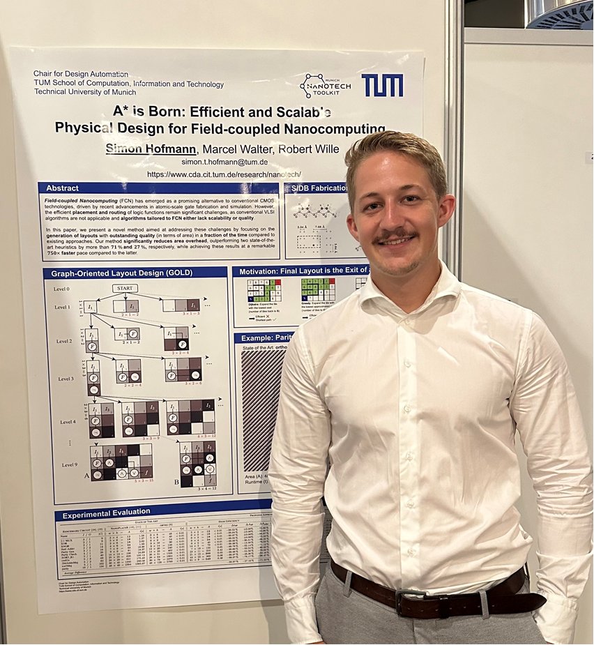
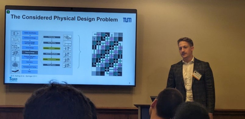
11 Jul 2024
A* is born! And his name is Simon Hofmann!😅 Seriously, A* obviously is a powerful method that has been very successfully used in #DesignAutomation in the past. Today at @IEEENANO_Conf, Simon showed how to use this potential also for the #PhysicalDesign for #FCN.
1/2

2
1
9
824
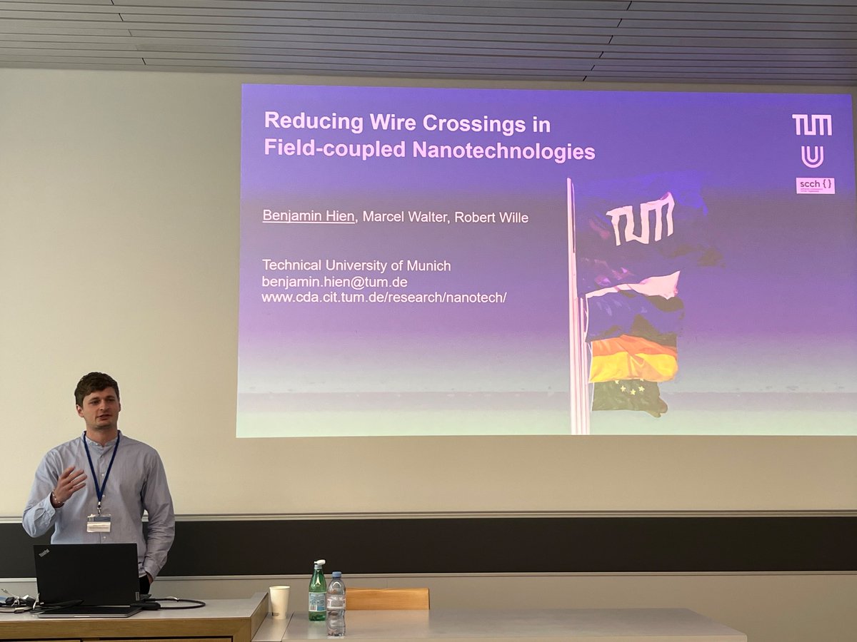
8 Jun 2024
In Field-Coupled Nanotechnologies #FCN, wire crossings are the reason for substantial costs. Accordingly, new #PhysicalDesign methods considering that are needed. Ideas how they could look like were proposed this week by Benjamin Hien and @MarcelCavani at the #IWLS workshop.
5
517
5 Apr 2024
Clocking constraints dominate the #PhysicalDesign for Field-coupled #Nanocomputing; and frequently put serious challenges in front of us. Now, Simon Hofmann (in a joint work with @ServadeiLorenzo and @MarcelCavani) came up with a brilliant idea: Think outside the clock!😉
1/2
1
1
12
542