
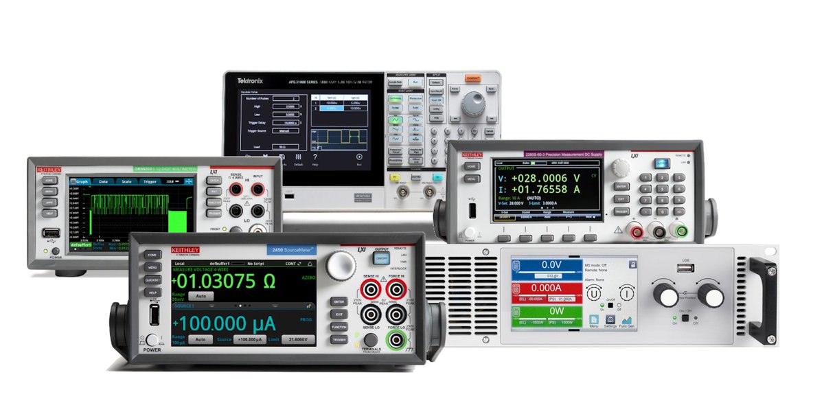
🙏 Thank you to everyone who visited the Chroma ATE booth at SWTest 2026!
It was a pleasure showcasing the Chroma 3530 Parametric Test System 🚀
🔗 Learn more: chromaus.com/parametric/3530
#SWTest2026 #ChromaATE #SemiconductorTesting #ParametricTest #WaferTest #Semiconductor

14

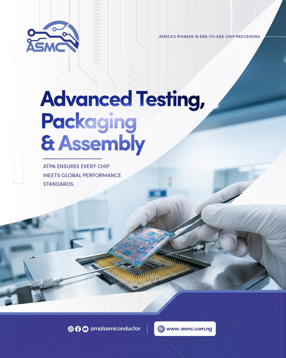
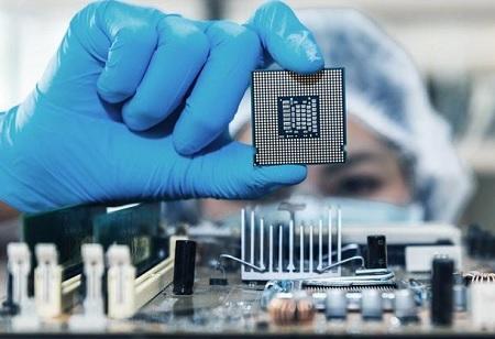
Advanced Testing, Packaging & Assembly ensures every chip meets global performance standards.
Discover how our ATPA processes deliver reliable, world-class semiconductor solutions.
#ASMC #ATPA #SemiconductorTesting #ChipPackaging #AdvancedManufacturing #EngineeringExcellence
2
4
269
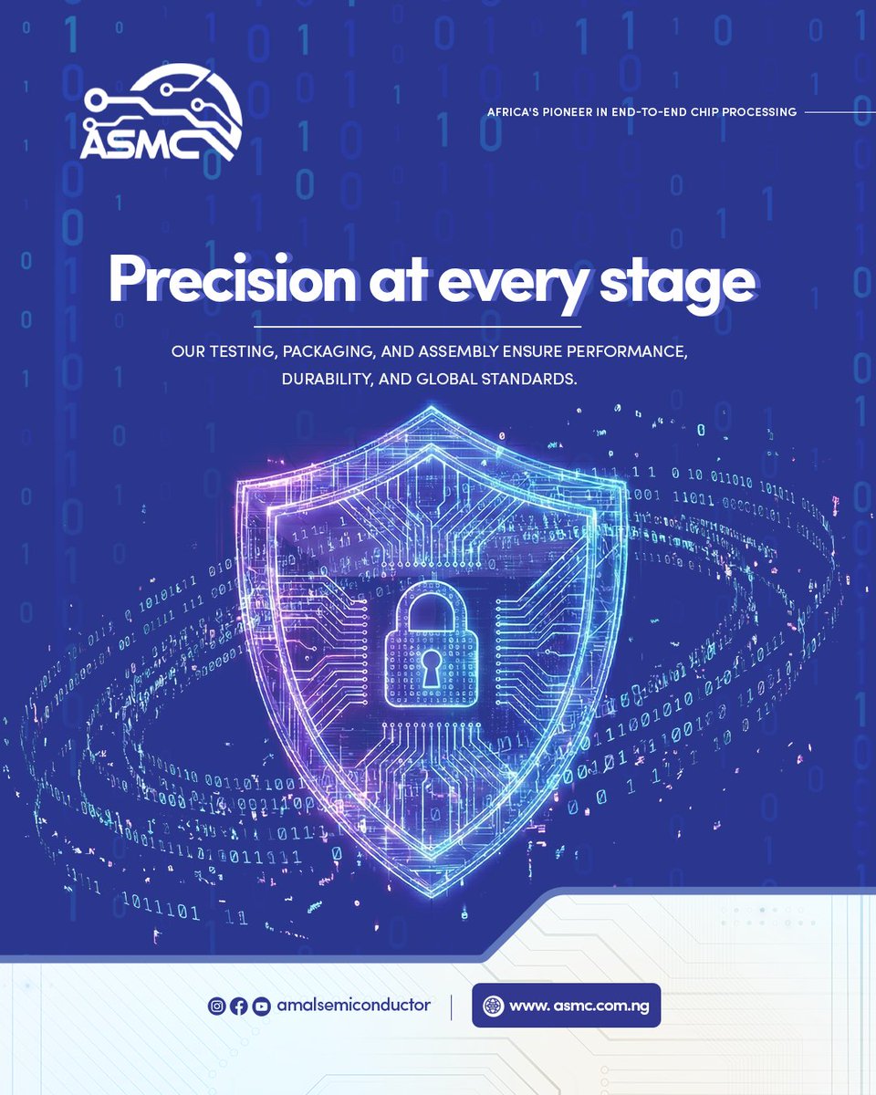
Precision at every stage. Our testing, packaging, and assembly ensure performance, durability, and global standards.
Learn more about our testing and packaging expertise at info@asmc.com.ng
#ASMC #SemiconductorTesting #ChipPackaging #AdvancedManufacturing
5
27

Mar 10
The Invisible Gatekeeper: Why Technoprobe $TPRO is the Master of Yield
The semiconductor industry has shifted its focus from "How fast can we make it?" to "How many can we actually sell?".
With 1.6T chips costing thousands of dollars to package, the financial penalty for a single defect is catastrophic. Technoprobe $TPRO, the Italian titan of micro-mechanics, has emerged as the mandatory gatekeeper of the AI supply chain.
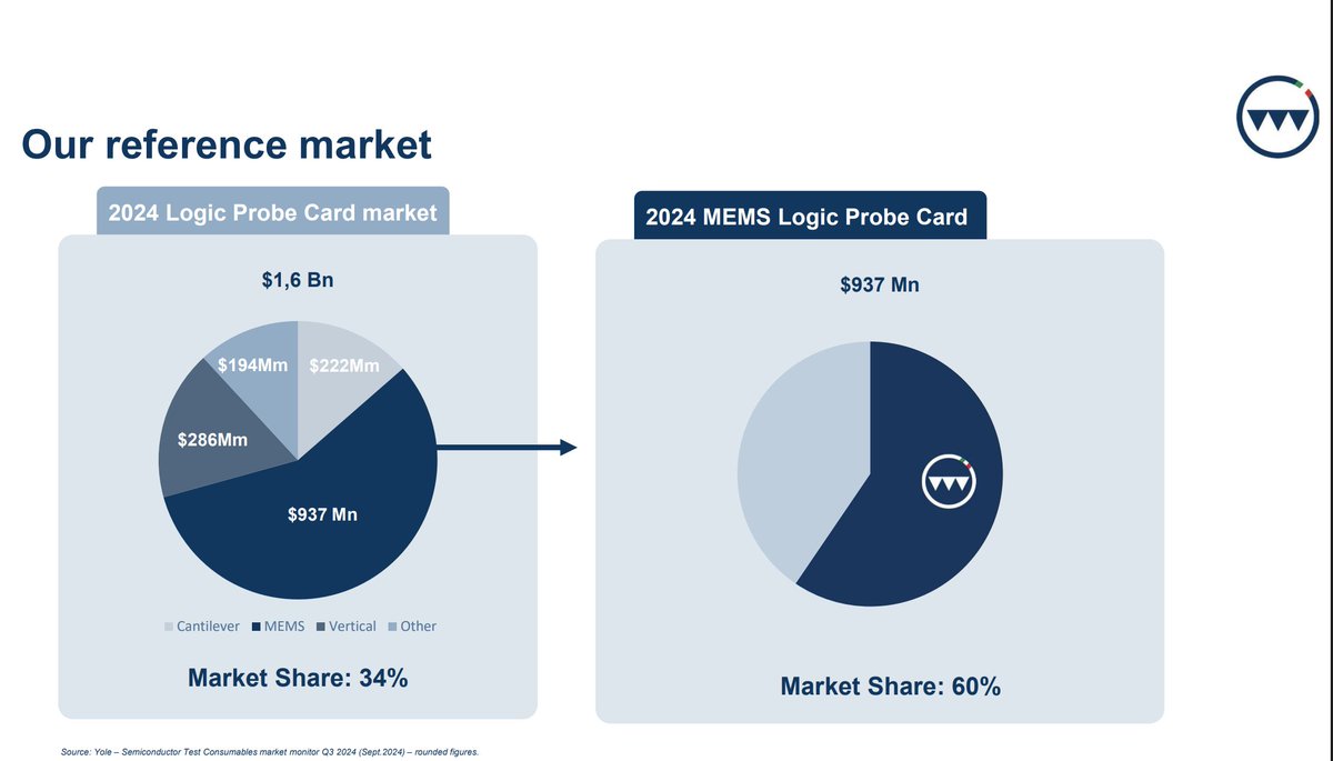
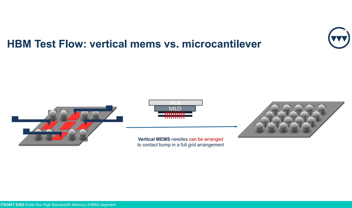
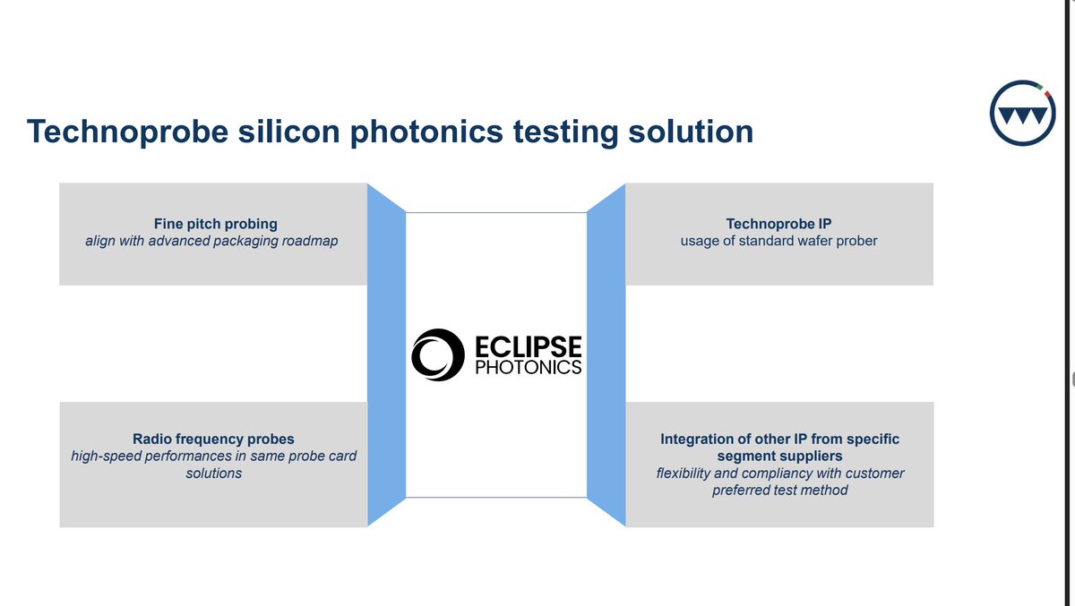
1⃣The Machine: T7000 & The MEMS Revolution
Technoprobe does not build the large test cabinets; they build the "eyes and fingers" that touch the silicon. Their Probe Cards are ultra-dense arrays of needles that verify chip integrity at the wafer level.
MEMS Dominance: At 1.6T speeds (224G per lane), traditional cantilever probes are obsolete. Technoprobe’s MEMS needles achieve a full-grid contact arrangement. Unlike traditional probes, they can test the entire surface of an HBM4-enabled chip simultaneously, ensuring 100% coverage for the ultra-dense interconnects of the 1.6T era.
Silicon Photonics Integration: In a landmark move on March 9, 2026, Technoprobe unveiled its Opto-Electrical Hybrid Card. This system tests both electrical and optical signals (lasers/light) directly on the wafer, a prerequisite for the Silicon Photonics pivot we see in 1.6T networking.
2⃣The Strategic Jackpot: The "NVIDIA Rubin" Catalyst
The Rubin Win: Industry insiders confirm Technoprobe has been qualified as the Primary Logic Probe Supplier for NVIDIA’s next-generation Rubin architecture. Rubin chips, which rely on HBM4 and 1.6T connectivity, require a level of test intensity that Technoprobe’s T7000 platform was specifically designed to handle.
This isn't just a speculation—industry giants Teradyne (10%) and Advantest (6%) are strategic shareholders, effectively cementing $TPRO as the universal standard for high-end AI testing.
FormFactor Rivalry: While the US-based FormFactor $FORM remains a leader in DRAM/HBM testing, Technoprobe has effectively captured over 45% of the Logic IC market share for advanced AI nodes, becoming the "Tool of Record" for TSMC’s N2 (2nm) process.
3⃣Financial Proof Points: Efficiency at Scale
Revenue Surge: Driven by the AI/HPC explosion, the company reported a 34.5% year-over-year increase in orders for Q4 2025/Q1 2026, significantly outpacing the broader ATE (Automatic Test Equipment) market.
Verified 9M 2025 actuals show a powerful operating leverage: while revenue grew by 20.6%, EBITDA skyrocketed by 53.3%. This margin expansion proves that the 1.6T complexity is a massive profit driver, not just a volume play
Fortress Balance Sheet: The company holds over €660M in net cash with virtually zero debt, providing the ammunition needed for strategic M&A in the burgeoning Silicon Photonics space.
4⃣The Bottleneck: Yield is the Only Currency
In the world of 1.6T, Yield is Profit. A 1% drop in yield on a 2nm line can result in $500M in lost annual revenue for a foundry.
The "Tax on Complexity": As chips become more complex (Chiplets, 3D Stacking), the number of test points increases exponentially. This makes Technoprobe a "tax" on every advanced chip produced; they don't just sell a machine once, they sell high-margin, consumable probe cards that wear out and must be replaced.
➡️Final Verdict: The Precision Monopoly
Technoprobe is the ultimate "pick and shovel" play for the 1.6T supercycle.
The Catalyst: With the NVIDIA Rubin production officially ramping up, all eyes are on Technoprobe’s full-year report on March 18, 2026. Watch for the "Inventory Surge" and "HBM segment" updates - this will likely be the official confirmation the market needs to re-rate $TPRO from a 'mobile-supplier' to a 'pure AI-infrastructure play'.
The Bull Case: They are the sole provider capable of high-volume testing for both the 2nm logic and the optical interconnects that define the 1.6T era. Their selection for the NVIDIA Rubin platform provides a multi-year growth runway.
The Risk: Heavy concentration in the foundry/logic segment. If the 2nm transition at Intel or Samsung faces further delays, Technoprobe’s logic revenue could see temporary volatility. However, the secular trend toward higher "test intensity" remains a powerful tailwind.
Summary: $TPRO provides the surgical precision required for the AI revolution. Without their "atomic-scale needles," the 1.6T dream would stay grounded by low yields and astronomical costs.
#TPRO #Technoprobe #1_6T #2nm #SemiconductorTesting #NVIDIA #YieldOptimization #Investing2026 #SiliconPhotonics


Atomic Precision: Why $ASMI is the Architect of the 1.6T Nanoworld
In the 1.6T infrastructure era, traditional manufacturing has hit a physical wall.
As the industry pivots to 2nm Gate-All-Around (GAA) transistors, depositing materials atom-by-atom is no longer a luxury - it is the ultimate bottleneck.
ASM International $ASMI has emerged as the gatekeeper of this transition, owning the tools that build the core of AI logic.
1⃣The Machine: Pulsar & Synergis (The ALD Standard)
Atomic Layer Deposition (ALD) is the process of building a chip one atomic layer at a time. For 1.6T networking and AI processors, ASMI’s systems are the industry benchmark:
➡️Pulsar® System: The "Tool of Record" for high-k metal gates. At the 2nm node, it ensures that dielectric layers are perfectly uniform to prevent current leakage in 1000W AI chips.
➡️GAA Architecture: The transition from FinFET to GAA nanosheets requires coating 3D structures that are physically impossible to reach with older methods. ASMI's ALD technology wraps the gate around the channel with angstrom-level precision, enabling the energy efficiency required for the 1.6T cycle.
➡️Epitaxy Synergy: ASMI's Intrepid® and Synergis® systems handle the critical "growing" of silicon-germanium layers for nanosheets, providing a dual-threat capability in both deposition and crystal growth.
2⃣ The Strategic Pivot: Area Selective Deposition (ASD)
ASMI has successfully moved Area Selective Deposition (ASD) from the lab to High-Volume Manufacturing (HVM).
The Breakthrough: ASD allows materials (like Molybdenum or advanced insulators) to "grow" only on specific chemical surfaces, eliminating the need for several costly lithography and etching steps.
1.6T Impact: Selective ALD reduces "edge placement errors" (EPE), which are the primary cause of signal noise in 224G-per-lane networking. ASMI currently holds a near-monopoly on the first wave of ASD tools deployed in 2nm fabs.
3⃣Investor Proof Points: Financial Reality ( last report 3rd March 2026)
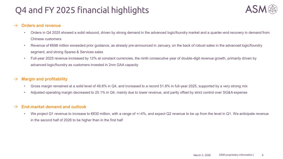
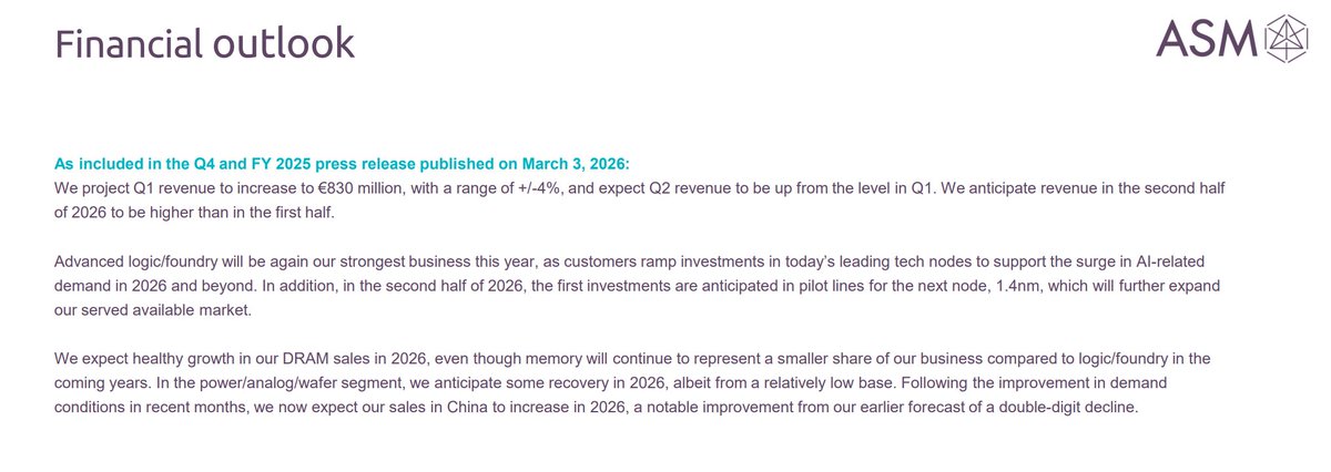
Record Revenue: ASMI ended 2025 with record revenue of €3.2 billion (up 12% at constant currencies), driven primarily by the 2nm GAA ramp-up.
Q1 2026 Guidance: Management officially projected Q1 2026 revenue of €830 million ( /- 4%), with a clear outlook for a stronger second half of 2026 as HBM4 memory orders accelerate.
Order Momentum: Q4 2025 bookings hit €803 million, significantly beating consensus estimates and signaling a massive rebound in logic/foundry demand.
Capital Return: The board has proposed an increased dividend of €3.25 per share (to be approved May 11, 2026) and a new €150 million share buyback program for 2026/2027.
4⃣ Competitive Moat: ASMI vs. The Giants
While Applied Materials $AMAT and Tokyo Electron are formidable, ASMI's niche focus gives it a tactical edge in the 1.6T stack:
The ALD Lead: ASMI controls over 55% of the global ALD market for logic. While AMAT is a leader in etch and CVD, ASMI’s "narrow and deep" expertise in atomic layers makes them indispensable for the 2nm gate stack.
Silicon Carbide (SiC) Recovery: Through its LPE subsidiary, ASMI is seeing a recovery in SiC epitaxy tools as AI data centers move toward more efficient power delivery systems, diversifying the company away from pure logic.
Final Verdict: The 2nm Yield Arbiter
ASMI is no longer a "growth story" - it is a Yield Arbiter. Without ASMI’s ALD and selective deposition, the 2nm node simply does not work.
Summary: The 1.6T era is defined by extreme density. By solving the patterning and insulation crises at the atomic level, $ASMI has secured its place as a mandatory partner for TSMC, Intel, and Samsung. For investors, ASMI represents the most direct way to play the materials science revolution that underpins the next decade of AI hardware.
#ASMI #ALD #Semiconductors #1_6T #2nm #GAA #Investing2026 #HighTechManufacturing #ASMLPartner

3
1
35
7,685

16 Dec 2025
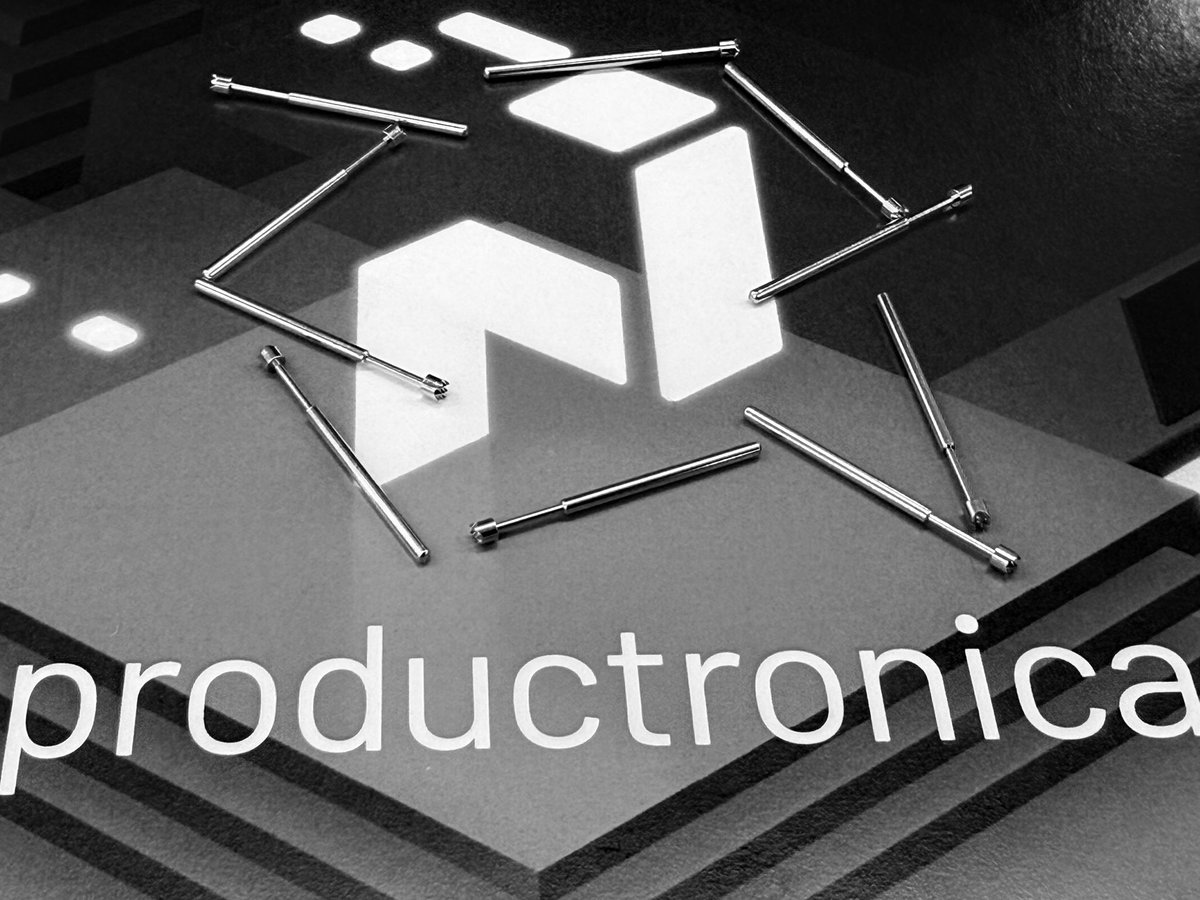
We participated for the 1st time in Productronica 2025 the world’s leading trade fair for electronics manufacturing. The event opened new opportunities for collaboration across the semiconductor industry.
#Productronica2025 #Seiken #SemiconductorTesting #ElectronicsManufacturing
1
21

5 Nov 2025
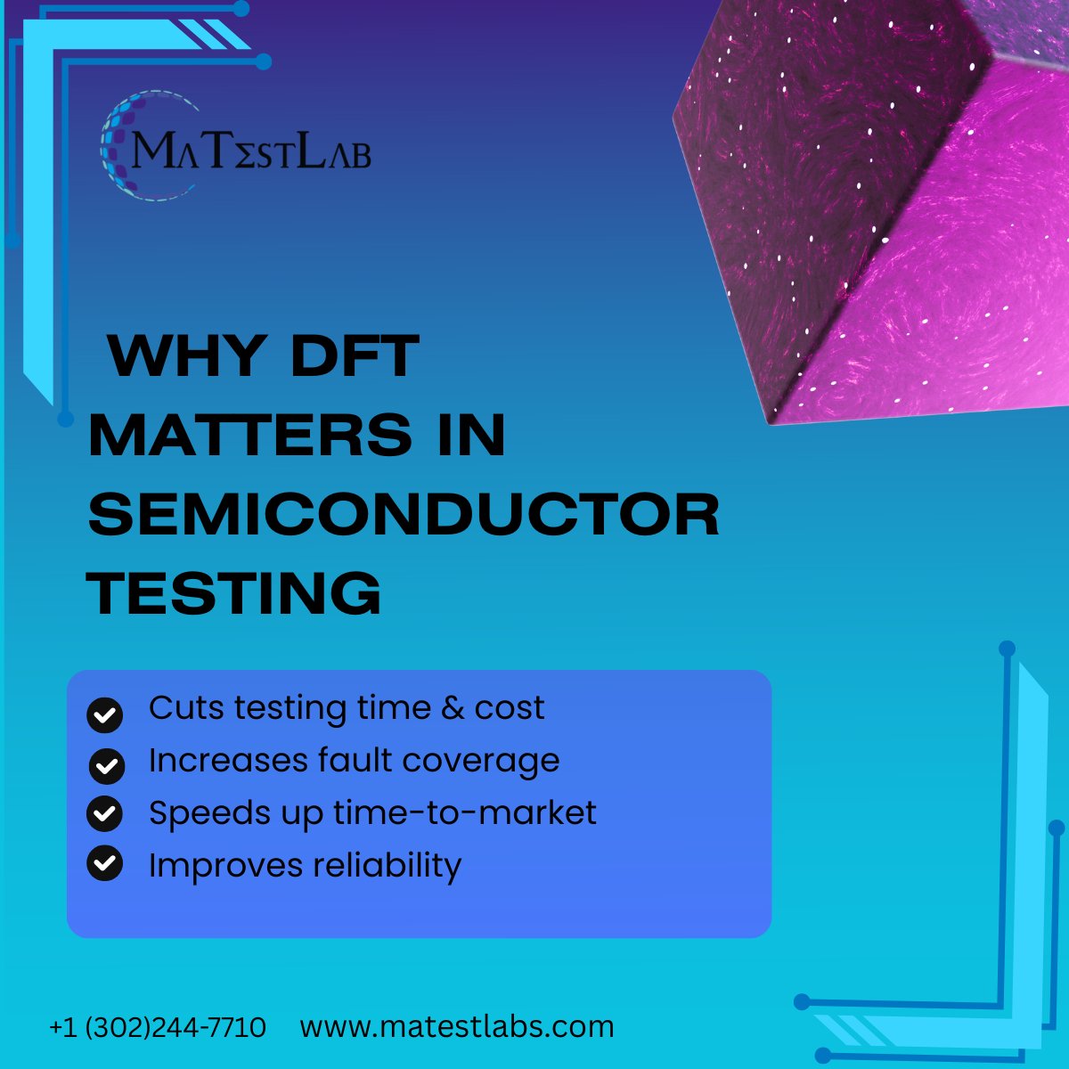
Design for Testability (DFT) is the practice of embedding test features inside a semiconductor chip. Instead of testing as an afterthought, the design is made test-friendly from the start.
#semiconductortesting #designfortestability #testautomation #innovationintesting
2
17

12 Aug 2025
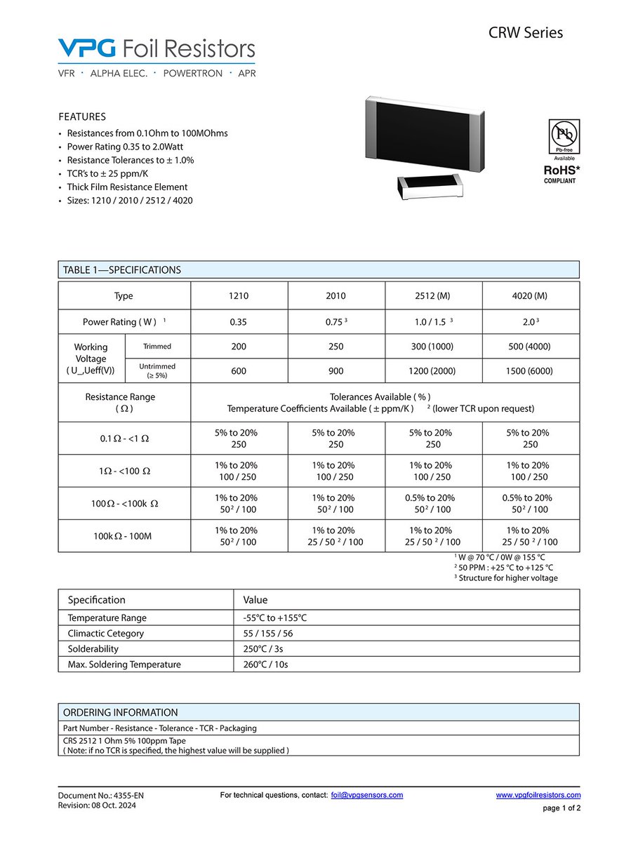
Resistor stability is non-negotiable in semiconductor testing.
The CRW Series offers:
- 0.1 Ω to 100 MΩ range
- To ±25 ppm/K TCR options
- Power ratings up to 2 W
- Long-term drift <1% at 70°C (1000 h)
For ATE and probe stations, these values help keep results consistent across temperature cycles and prolonged testing.
For more information about our Surface Mount resistors: tinyurl.com/v9p45jds
How do you ensure resistor stability in your precision measurement setups?
#TestAndMeasurement #SemiconductorTesting #SurfaceMount #PrecisionResistors #CRWSeries #VPGFoilResistors

1
2
48

24 Jun 2025
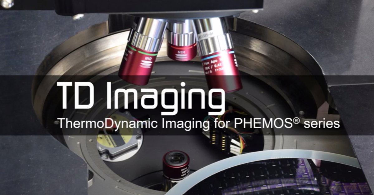
#Demo alert! Hamamatsu is now accepting requests for ThermoDynamic Imaging (TD Imaging) demos!
👉 Request your personalized demo here: ow.ly/rrie50W94Yn
#FailureAnalysis #SemiconductorTesting #ThermalImaging #Hamamatsu
3
367


20 Feb 2025
SMUs: The versatile powerhouse of test & measurement.
From precision sourcing to 4-quadrant operation, SMUs go beyond power supplies, loads, and DMMs. See how they optimize your test setups: bit.ly/4huP4pT
#TestAndMeasurement #EngineeringSolutions #SemiconductorTesting
4
267

18 Sep 2024
🌟 @SolitonTech is revolutionizing semiconductor testing with AI & automation! With 26 years of expertise, they lead in innovation and efficiency. Discover more in our latest interview! 🚀 #SemiconductorTesting #Automation #AI @alok_nayak @YoursShakti theinterview.world/driving-q…
2
3
49

30 Jan 2024
US Export Regulations Prompt Shift of Manufacturing Away from China
News: rb.gy/lstlof
Brian Amero, Teradyne's Director of Global Compliance and Ethics
#semiconductortesting #semiconductor #UStechnology #Chinesemilitary
3
111

28 Sep 2023
The @MicronTech is set to begin construction for its semiconductor testing and assembly plant in Sanand, Gujarat.
Read more: tele.net.in/micron-to-begin-…
#semiconductors #semiconductorindia #semiconductormanufacturing #semiconductorplant #semiconductortesting #fabricationunit
2
105

27 Apr 2022
Thank you, Advantest for hosting Nir Sever, proteanTecs Senior Director of Business Development at your ACS Open Solutions Ecosystem symposium today.
Presenting with partners is the best!
#universalchiptelemetry #advancedanalytics #semiconductortesting #deepdata

2