How Does a Digital Multimeter Work? - Understand the Essentials.
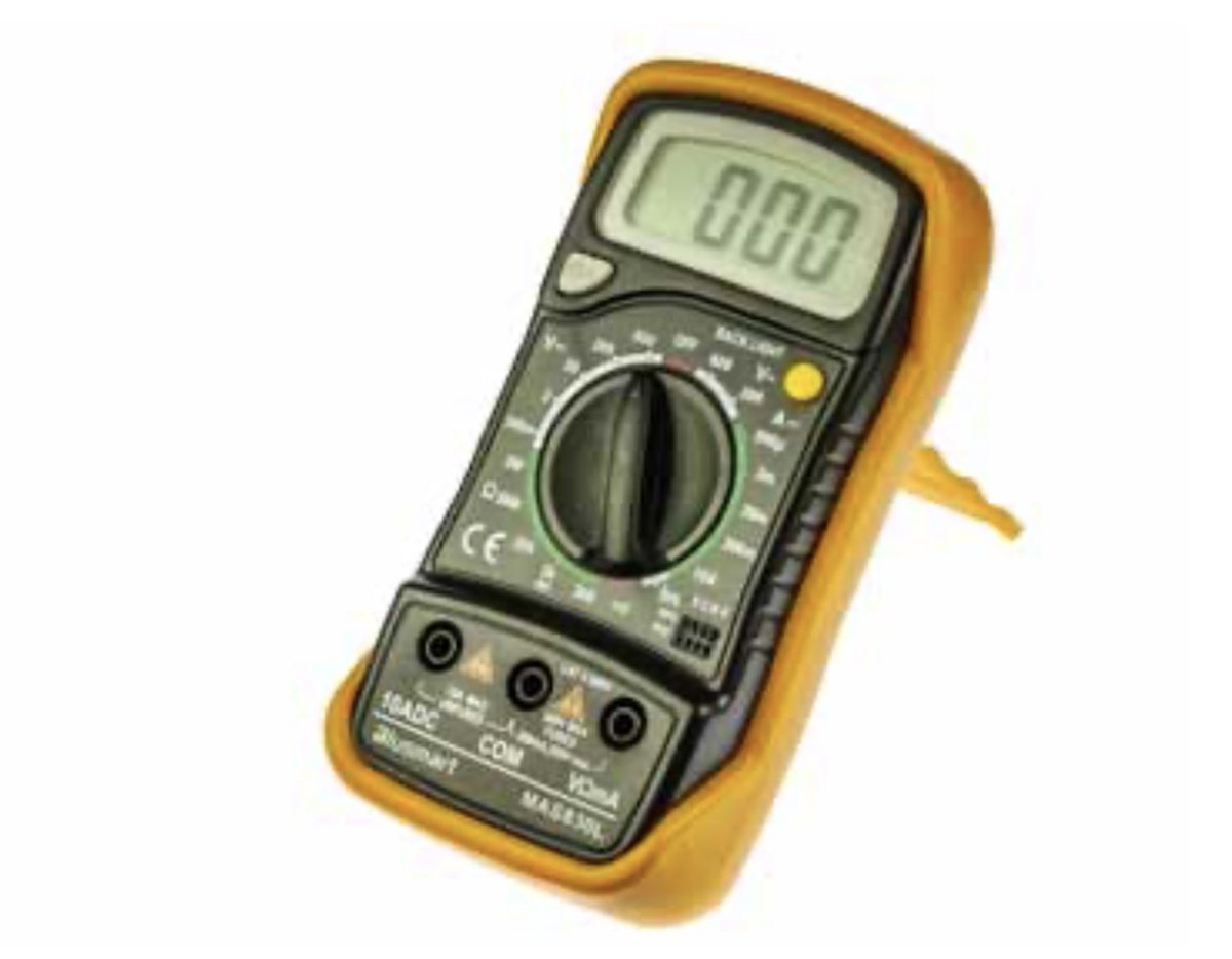
Have you ever wondered what’s actually happening inside your Digital Multimeter (DMM) when you probe a circuit?
While it looks like a simple digital screen replacing an old analogue needle, the "magic" inside is a fascinating process of high-speed translation.
Based on the expert insights from Electronics Notes, here is a breakdown of how your DMM actually works:
1. The Core: The ADC (Analog-to-Digital Converter)
The heart of every DMM is the ADC. Most general-purpose multimeters use a Successive Approximation Register (SAR).
• Think of it like a game of "Higher or Lower."
• The ADC compares the input voltage to a reference voltage, starting at half-scale and narrowing it down bit-by-bit until it "homes in" on the exact value.
2. Signal Pre-Conditioning
The ADC can only handle a specific, small range of voltage. To measure different things, the DMM "prepares" the signal:
• Voltage: Uses potential divider networks to scale high voltages down to a range the ADC can handle.
• Current: Measures the voltage drop across a known internal resistor (a shunt) and then calculates the current using Ohm’s Law.
• Resistance: Passes a small, known current through the component and measures the resulting voltage drop.
3. Buffering and Averaging
Ever notice why the numbers don’t jump around frantically? The DMM doesn't just show one raw sample. It buffers and averages multiple samples to filter out electrical noise, ensuring the reading you see on the LCD is stable and accurate.
4. The "Settling Time" Factor
When you switch ranges or probes, the internal circuitry needs time to stabilize. This is why the reading might "climb" for a split second before staying still. High-end meters also perform an Auto-Zero to ensure there’s no offset error before giving you the final result.
Pro Tip: Understanding this process helps you realize why "settling time" matters—especially when using computer-controlled test equipment where timing is everything!
🔗 For a full explanation, check the link to my website in the comments.
#Electronics #Engineering #TestEquipment #DigitalMultimeter #EmbeddedSystems #LearningElectronics #electronicsnotes

2
3
48
1,704
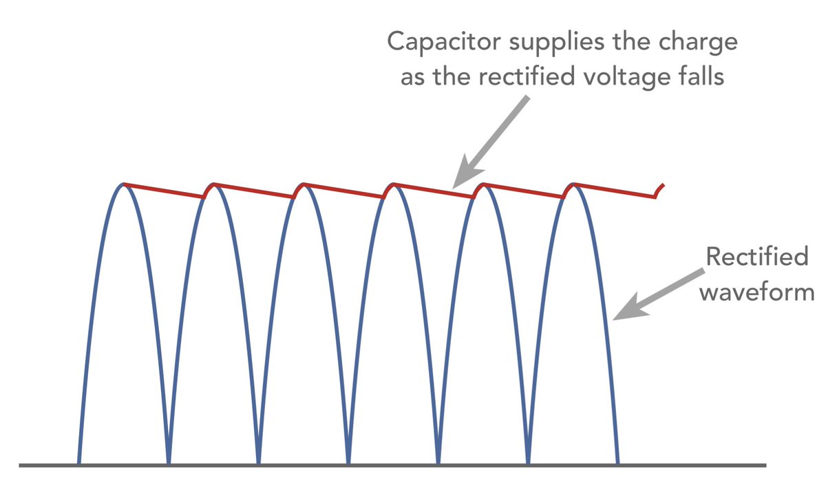
Power Supply Smoothing: the key facts you need to know
Turning raw rectified AC power into the smooth DC that powers our sensitive electronics is a key technique in any analogue power supply.
The secret lies in a very important component: the Smoothing (or Reservoir) Capacitor.
Let’s take a look at why these components are able to provide essential smoothing in both linear and switch-mode power supplies.
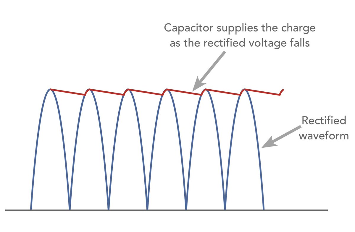
If you’ve ever seen a "raw" rectified waveform, you know it’s a series of peaks and valleys - basically useless for either an analogue or digital circuit.
Here are the key takeaways from the full article:
✅ The "Gap Filler" Effect: A smoothing capacitor acts like a temporary battery. It charges up during the voltage peaks and discharges its stored energy when the rectifier voltage drops. This "fills in the dips," resulting in a much steadier DC output.
✅ The Ripple Reality: Total stability is a myth. There will always be some "ripple voltage." The trick to minimizing it? A larger capacitor value and a higher ripple frequency (which is why full-wave rectification is always preferred over half-wave). But beware as the capacitor gets larger, so the charge spikes where the capacitor charges up become shorter and the current higher.
✅ The Critical Calculation:
Choosing the right value isn't guesswork. The time constant (R C) must be significantly longer than the time between peaks. For a full-wave rectifier:
V_(ripple) = I_(load) / (2fC)
✅ The Hidden Danger: Ripple Current:
This is where many designs fail. The capacitor doesn’t just sit there; it handles intense bursts of current during the charging phase. If you exceed the "Ripple Current Rating," your capacitor will heat up, its lifespan will plummet, and it could even fail catastrophically.
✅ Why Electrolytics Rule:
Aluminum electrolytic capacitors are the standard here. They offer the high capacitance needed to handle large currents at a cost-effective price point.
Whether you are designing a high-end audio amp or a simple DIY power supply, understanding the relationship between load, frequency, and capacitance is vital for a stable, long-lasting circuit.
Want to see the calculations and the circuit diagrams behind this?
Check out the link in the comments for more information.
#ElectronicsEngineering #PowerSupply #CircuitDesign #ElectricalEngineering #electronicsnotes #LearningElectronics

1
11
88
3,622
We all use them, but how do they work: the PN junction diode.
The PN junction diode is arguably one of the most important building blocks in modern electronics.
I’ve just put together this summary of the PN Junction Diode based on my resources at Electronics Notes. Whether you’re a student, a hobbyist, or a seasoned engineer, understanding the "why" behind the "how" of this component is essential.
The Discovery
The diode or PN junction was the first form of semiconductor device to be investigated in the early 1940s when the first real research was undertaken into semiconductor technology. It was found that small point contact diodes were able to rectify some of the microwave frequencies used in early radar systems and as a result they soon found many uses.
How It Works: The Basics
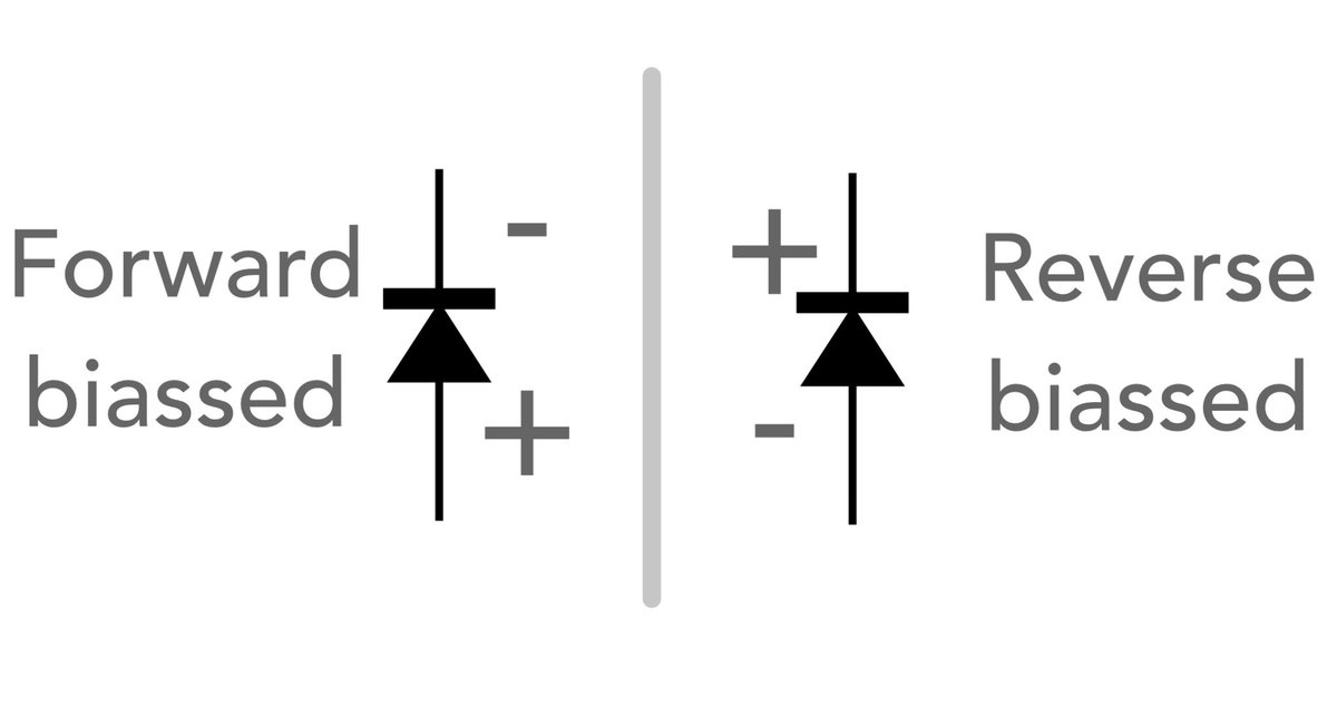
At its core, a PN junction is formed by joining P-type (positive charge carriers/holes) and N-type (negative charge carriers/electrons) semiconductor materials.
• The Depletion Region: When joined, electrons and holes near the junction neutralize each other, creating a "barrier" with no free charge carriers.
• Forward Bias: Apply a positive voltage to the P-type (Anode) and negative to the N-type (Cathode), and you "push" the carriers across the barrier. Current flows!
• Reverse Bias: Flip the polarity, and you pull the carriers away from the junction, widening the depletion region. The result? The diode acts as an insulator, blocking current.
Why It Matters
While we often think of diodes as simple "one-way valves" for electricity, their impact is much broader:
1. Rectification: Converting AC to DC—the heart of every power supply.
2. Signal Demodulation: Essential for radio communications.
3. The Foundation of Everything: The PN junction isn't just in discrete diodes; it’s the fundamental element inside Bipolar Transistors (BJTs), FETs, and billions of transistors within integrated circuits.
Pro-Tip for Circuit Designers
When selecting a diode, don't just look at the current rating. Remember the Forward Voltage Drop (typically 0.6V for the turn on voltage for Silicon) and the Peak Inverse Voltage (PIV). Running a diode too close to its maximum ratings can significantly impact the long-term reliability of your PCB.
If you want to brush up on the full physics, IV characteristics, and invention history, check out the full article in the link in the comments.
#Electronics #electroniccomponents #diode #PNjunction #Semiconductors #ElectricalEngineering #LearningElectronics #STEM #electronicsnotes

3
6
33
1,370
Understand How Your Digital Multimeter Works - You Need to Know So You Can Use It Properly.
Have you ever wondered what’s actually happening inside your Digital Multimeter (DMM) when you probe a circuit?
While it looks like a simple digital screen replacing an old analogue needle, the "magic" inside is a fascinating process of high-speed translation.
Based on the expert insights from Electronics Notes, here is a breakdown of how your DMM actually works:
1. The Core: The ADC (Analog-to-Digital Converter)
The heart of every DMM is the ADC. Most general-purpose multimeters use a Successive Approximation Register (SAR).
• Think of it like a game of "Higher or Lower."
• The ADC compares the input voltage to a reference voltage, starting at half-scale and narrowing it down bit-by-bit until it "homes in" on the exact value.
2. Signal Pre-Conditioning
The ADC can only handle a specific, small range of voltage. To measure different things, the DMM "prepares" the signal:
• Voltage: Uses potential divider networks to scale high voltages down to a range the ADC can handle.
• Current: Measures the voltage drop across a known internal resistor (a shunt) and then calculates the current using Ohm’s Law.
• Resistance: Passes a small, known current through the component and measures the resulting voltage drop.
3. Buffering and Averaging
Ever notice why the numbers don’t jump around frantically? The DMM doesn't just show one raw sample. It buffers and averages multiple samples to filter out electrical noise, ensuring the reading you see on the LCD is stable and accurate.
4. The "Settling Time" Factor
When you switch ranges or probes, the internal circuitry needs time to stabilize. This is why the reading might "climb" for a split second before staying still. High-end meters also perform an Auto-Zero to ensure there’s no offset error before giving you the final result.
Pro Tip: Understanding this process helps you realize why "settling time" matters—especially when using computer-controlled test equipment where timing is everything!
🔗 For a full explanation, check the link to my website in the comments.
#Electronics #Engineering #TestEquipment #DigitalMultimeter #EmbeddedSystems #LearningElectronics #electronicsnotes
2
6
38
2,158
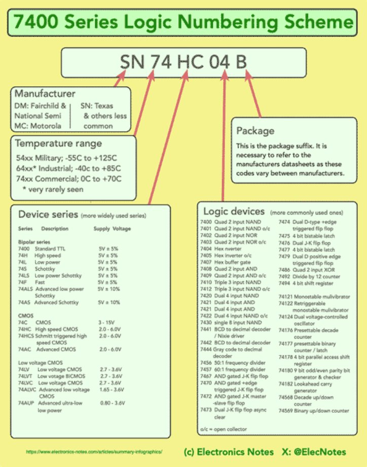
Do You Understand the 74xx Series Logic Part Numbering?
Decoding the 7400 series is a rite of passage for every electronics engineer and hobbyist. Ever looked at a chip and wondered what the difference between a SN74LS00N and a 74HC00 really is?
It’s not just a random string of characters—it's a precise shorthand that tells you the manufacturer, the logic technology, the speed, the power consumption, and the physical footprint of the chip.
This excellent infographic from Electronics Notes breaks down the "secret code" of 7400 series logic:
🔹 Prefix (e.g., SN): Identifies the manufacturer (Texas Instruments in this case).
🔹 Series (74 vs 54): 74 is for commercial grade, while 54 is built for military/harsh environments.
🔹 Family (e.g., LS, HC, HCT): This is the "engine" of the chip. Whether it’s Low-power Schottky (LS) or High-speed CMOS (HC), this determines how fast it switches and how much power it draws.
🔹 Function (e.g., 00, 32, 74): The core identity—tells you if you're holding a NAND gate, an OR gate, or a D-type Flip-flop.
🔹 Suffix (e.g., N, D, J): Defines the package type, from classic through-hole DIP to modern surface-mount SOIC.
Whether you're restoring a vintage computer or prototyping on a breadboard, having this "decoder ring" nearby is a huge time-saver.
Check out the full guide and infographic here: 🔗 electronics-notes.com/articl…
#Electronics #Engineering #DigitalLogic #7400Series #HardwareDesign #LearningElectronics #PCBDesign #Electroniccomponents #ElectronicsNotes
3
33
143
5,878
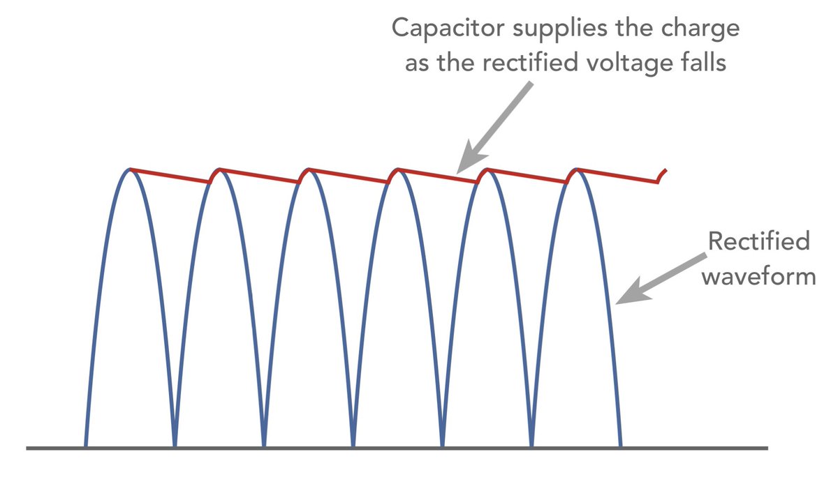
Understanding Power Supply Smoothing
Turning raw rectified AC power into the smooth DC that powers our sensitive electronics is a key technique in any analogue power supply.
The secret lies in a very important component: the Smoothing (or Reservoir) Capacitor.
Let’s take a look at why these components are able to provide essential smoothing in both linear and switch-mode power supplies.
If you’ve ever seen a "raw" rectified waveform, you know it’s a series of peaks and valleys - basically useless for either an analogue or digital circuit.
Here are the key takeaways from the full article:
✅ The "Gap Filler" Effect: A smoothing capacitor acts like a temporary battery. It charges up during the voltage peaks and discharges its stored energy when the rectifier voltage drops. This "fills in the dips," resulting in a much steadier DC output.
✅ The Ripple Reality: Total stability is a myth. There will always be some "ripple voltage." The trick to minimizing it? A larger capacitor value and a higher ripple frequency (which is why full-wave rectification is always preferred over half-wave).
✅ The Critical Calculation:
Choosing the right value isn't guesswork. The time constant (R \times C) must be significantly longer than the time between peaks. For a full-wave rectifier:
V_(ripple) = I_(load) / (2fC)
✅ The Hidden Danger: Ripple Current:
This is where many designs fail. The capacitor doesn’t just sit there; it handles intense bursts of current during the charging phase. If you exceed the "Ripple Current Rating," your capacitor will heat up, its lifespan will plummet, and it could even fail catastrophically.
✅ Why Electrolytics Rule:
Aluminum electrolytic capacitors are the standard here. They offer the high capacitance needed to handle large currents at a cost-effective price point.
Whether you are designing a high-end audio amp or a simple DIY power supply, understanding the relationship between load, frequency, and capacitance is vital for a stable, long-lasting circuit.
Want to see the calculations and the circuit diagrams behind this?
Check out the link in the comments for more information.
#ElectronicsEngineering #PowerSupply #CircuitDesign #ElectricalEngineering #electronicsnotes #LearningElectronics
2
8
77
2,925
Did you ever own a valve / tube radio?
When I was a schoolboy with little money and people knew of my interest in radio, I would often be given radios by people who said: If you can fix it we'll have it back otherwise you can have it for the bits.
Needless to say, with little test equipment and only learning about electronics, I could rarely fix them. But I often spent a lot of my money on parts to try to get them going, only to fail.
But what did happen occasionally was I was given something that was working. One such radio was a Decca Portrola 52. This was was a semi-portable radiogram (combination of radio & gramophone) launched in 1952 providing reasonable quality reproduction and long & medium wave radio coverage. I think I was given it around 1966.
I could even tune it down to the bottom of the medium wave band and catch the odd amateur radio transmission on 160 metres.
I often listenied to the pirate radio stations that were popular around the UK at that time. As for the record player (vinyl player) section, it was rather old and I'm sure I ruined many a vinyl record on it, but it played the music.
Unfortunately I don't have any photos of the equipment, so this diagram I drew is the best I can do,.
Do you have any radios which were part of your youth, and possibly you introduction to radio and technology?
#electronics #vintageradio #valves #tubes #vacuumtubes #learningelectronics #electronicsnotes

9
1
22
1,492
What’s the one piece of advice you’d give to yourself on Day 1 of your career in electronics?
I’ll start: 'Check the datasheet. Then check it again. Then check the ERRATA.
#electronics #learningelectronics #electronicscareer #electronicsadvice #electronicstips
7
2
48
2,009
Why your DC power supply is only as good as its Reservoir Capacitor
Ever wondered how we turn "bumpy" rectified AC into the smooth DC required by sensitive electronics? It all comes down to the Capacitor Smoothing Circuit.
In both linear and switch-mode power supplies, the rectifier output consists of a series of half-sine waves.
Without smoothing, digital circuits would lose power every half-cycle, and analog circuits would be plagued by hum and noise.
Here are 3 key takeaways for engineers and hobbyists on getting smoothing right:
1️⃣ The "Fill in the Gaps" Strategy:
A reservoir capacitor (typically an aluminum electrolytic) works by charging up at the voltage peak and discharging into the load when the rectifier voltage drops. Essentially, it "fills in the dips" to maintain a steady output.
2️⃣ Full-Wave vs. Half-Wave:
Efficiency matters! Full-wave rectification is always preferable because the gaps between peaks are shorter. This leads to significantly better smoothing and allows for a smaller capacitor to achieve the same ripple voltage.
3️⃣ Don't ignore Ripple Current!
When choosing a capacitor, capacitance and voltage aren't the only specs that matter. You must check the Maximum Ripple Current.
* Because the capacitor only charges during a very short window of the cycle, the peak charging current can be much higher than the steady-state load current.
* Overlooking this leads to overheating, reduced lifespan, or even catastrophic failure.
Pro-tip for the maths: To estimate peak-to-peak ripple Vripple for a full-wave rectifier, use:
👉 Vripple = Iload / (2 f C)
Looking to go deeper into the calculations and filters? Check out the link in the comments.
#ElectronicsEngineering #PowerSupply #CircuitDesign #ElectricalEngineering #electronicsnotes #electroniccomponents #LearningElectronics
1
6
39
1,665
The PN junction diode is arguably one of the most important building blocks in modern electronics.
I’ve just put together this summary of the PN Junction Diode based on my resources at Electronics Notes. Whether you’re a student, a hobbyist, or a seasoned engineer, understanding the "why" behind the "how" of this component is essential.
The Discovery
The diode or PN junction was the first form of semiconductor device to be investigated in the early 1940s when the first real research was undertaken into semiconductor technology. It was found that small point contact diodes were able to rectify some of the microwave frequencies used in early radar systems and as a result they soon found many uses.
🔍 How It Works: The Basics
At its core, a PN junction is formed by joining P-type (positive charge carriers/holes) and N-type (negative charge carriers/electrons) semiconductor materials.
• The Depletion Region: When joined, electrons and holes near the junction neutralize each other, creating a "barrier" with no free charge carriers.
• Forward Bias: Apply a positive voltage to the P-type (Anode) and negative to the N-type (Cathode), and you "push" the carriers across the barrier. Current flows!
• Reverse Bias: Flip the polarity, and you pull the carriers away from the junction, widening the depletion region. The result? The diode acts as an insulator, blocking current.
Why It Matters
While we often think of diodes as simple "one-way valves" for electricity, their impact is much broader:
1. Rectification: Converting AC to DC—the heart of every power supply.
2. Signal Demodulation: Essential for radio communications.
3. The Foundation of Everything: The PN junction isn't just in discrete diodes; it’s the fundamental element inside Bipolar Transistors (BJTs), FETs, and billions of transistors within integrated circuits.
Pro-Tip for Circuit Designers
When selecting a diode, don't just look at the current rating. Remember the Forward Voltage Drop (typically 0.6V for the turn on voltage for Silicon) and the Peak Inverse Voltage (PIV). Running a diode too close to its maximum ratings can significantly impact the long-term reliability of your PCB.
If you want to brush up on the full physics, IV characteristics, and invention history, check out the full article in the link in the comments.
#Electronics #electroniccomponents #Semiconductors #ElectricalEngineering #LearningElectronics #STEM #electronicsnotes
2
5
43
2,083

26 Dec 2025
Ever wondered how to turn raw rectified AC power into the smooth DC that powers our sensitive electronics?
The secret lies in a small but mighty component: The Smoothing (or Reservoir) Capacitor.
Let’s take a look at why these components are able to provide essential smoothing in both linear and switch-mode power supplies.
If you’ve ever seen a "raw" rectified waveform, you know it’s a series of peaks and valleys—basically useless for a digital circuit.
Here are the key takeaways from the full article:
✅ The "Gap Filler" Effect: A smoothing capacitor acts like a temporary battery. It charges up during the voltage peaks and discharges its stored energy when the rectifier voltage drops. This "fills in the dips," resulting in a much steadier DC output.
✅ The Ripple Reality: Total stability is a myth. There will always be some "ripple voltage." The trick to minimizing it? A larger capacitor value and a higher ripple frequency (which is why full-wave rectification is always preferred over half-wave).
✅ The Critical Calculation:
Choosing the right value isn't guesswork. The time constant (R \times C) must be significantly longer than the time between peaks. For a full-wave rectifier:
V_{ripple} = I_{load) / (2fC}
✅ The Hidden Danger: Ripple Current:
This is where many designs fail. The capacitor doesn’t just sit there; it handles intense bursts of current during the charging phase. If you exceed the "Ripple Current Rating," your capacitor will heat up, its lifespan will plummet, and it could even fail catastrophically.
✅ Why Electrolytics Rule:
Aluminum electrolytic capacitors are the standard here. They offer the high capacitance needed to handle large currents at a cost-effective price point.
Whether you are designing a high-end audio amp or a simple DIY power supply, understanding the relationship between load, frequency, and capacitance is vital for a stable, long-lasting circuit.
Want to see the calculations and the circuit diagrams behind this?
Check out the link in the comments for more information.
#ElectronicsEngineering #PowerSupply #CircuitDesign #ElectricalEngineering #EmbeddedSystems #LearningElectronics
6
20
161
7,001

8 Jan 2024
Understanding the basics of electronic devices is crucial in today's tech-driven world. Begin with learning about components like resistors, capacitors, and semiconductors.
Explore circuitry and how devices process information. Familiarize yourself with common electronic terms like voltage, current, and resistance.
Delve into digital and analog signals, understanding their applications. Learn about different types of electronic devices, from simple circuits to complex microcontrollers.
Gain hands-on experience through practical projects to reinforce theoretical knowledge. As you build a foundation, you'll be better equipped to navigate the diverse landscape of electronic devices. #ElectronicsBasics #TechKnowledge #LearningElectronics
16
2
294

28 Jan 2023
Builder's Sunday at EdVenture Park.
#flywithevp
#hyderabadincubator #education #telangananews #tsktransformation #school #education #teacher #learningelectronics #startupindia #startupbusiness #studentstartup #studentstartups #hardwarelab #projects #hardwaretools

7
482

24 Nov 2022
ECE MINI/MICRO PROJECTS | ELECTRICAL ENGINEERING PROJECTS |
.
.
.
.
.
@LEARNINGELECTRONICS
#electronics #technology #tech #engineering #gadgets #iphone #electrical #arduino #electronic #instagood #robotics #instatech #electricalengineering #gadget
2
5
26 Jul 2022
Darkness detector 🧐
.
.
#LearningElectronics #electrosoftsystem #machine #speed #science #gadgets #technology #sensors #LDR
watch full video on YouTube
click on given link 👇👇
youtu.be/UI_osibN8Zs
1
3
23 Jul 2022
Manual peeling of the cover
@LearningElectr2
#LearningElectronics #trending #science #Tweeter #reels #manual #peeling #memory #memorycard #gadgets #technology #zoom
3
22 Jul 2022
Propeller globe..⚡🔮🔮
.
.
#cessna152 #piperaircraft #aircraft #aeroplane #helicopters #aeroplanes #rcplane #plane #flying #cockpit
#msccargoa #flight #aviation #LearningElectronics #electrosoftsystem #propellerdisplay #science #gadgets
2
21 Jul 2022
Automatic paper feeding system..👍
.
.
@LearningElectr2
#LearningElectronics #electrosoft #jalgaon #electrosoftsystem #lightroom #ledlights #technology #MicrosoftTeams #follow #famous #treanding #automation
2
19 Jul 2022
Ultrasonic levitation 🤩🔮🔮
.
.
.
#LearningElectronics #electrosoft #electrosoftsystem #FolloForFolloBack #treanding #Tweeter #ultrasonic #science
1
2

5 Jan 2021
Seguimos con nuestras andanzas en Arduino para ignorantes. #Arduino #Twitchstreamer #electronics #learningelectronics twitch.tv/dreparar
1
2