
Joined April 2016
- Tweets 10,297
- Following 457
- Followers 3,800
- Likes 42,236
406 Photos and videos


Pinned Tweet

Thanks for 3k followers!
저는 InP 계열의 포토닉스 산업 종사자였습니다.
반도체, crystallography 및 quantum tech(ex. Quantum computing, QKD, Quantum sensing)에 관한 글도 종종 작성합니다.
또한 요즘엔 AI 프롬프트 개발에 관해서도 많은 관심을 가지고 있으며, 그 외에 소소한 일상도 공유하고 있습니다.
앞으로도 잘 부탁드립니다🥰
今後ともよろしくお願いします🥰
17
3
63
5,841

>>MLCC Industry Faces "Longest Shortage Cycle in History"… Supply Deficit Expected to Persist Beyond 2027
- Major Taiwanese MLCC makers—Yageo, Walsin, Holy Stone, and PDC—are strongly upbeat on the industry outlook, driven by AI demand. The industry believes this shortage could surpass the 2018 passive component supercycle.
- Walsin in particular projected that the MLCC shortage could persist beyond 2027. The company expects demand to rise even further once AI PCs and AI edge devices—markets far larger than AI servers—begin to proliferate in earnest.
- Yageo's book-to-bill (BB) ratio has already moved above 1.3x, and the company is responding to rising orders by ramping line utilization and clearing bottlenecks.
- That said, the pace of capacity expansion is constrained by equipment shortages. According to Holy Stone, lead times for high-end MLCC production equipment run 1 to 1.5 years, making capacity additions difficult. Holy Stone expects capacity to grow 20~30% YoY this year and a further 30~40% in 2027, but warned that next year's supply shortage could in fact intensify.
- Walsin is likewise tripling CAPEX this year and pursuing capacity expansion for a second consecutive year, but noted that lead times from Japanese equipment vendors run 6 to 12 months, making it hard for supply growth to keep pace with demand. AI infrastructure demand, in its view, is only just beginning.
15
46
279
49,279
슈포 (Superposition) retweeted

10h
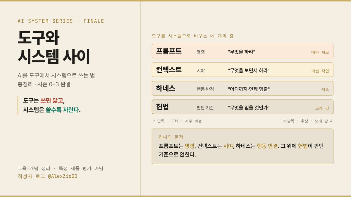
AI를 도구에서 시스템으로 쓰는 법. 21편이 오늘 끝났습니다.
4주에 걸쳐 주말마다 5편씩, 한 세트가 한 주제였고, 일부러 이렇게 짰습니다.
헌법, 프롬프트, 컨텍스트, 하네스. 네 개를 따로따로 흩어 올리면 독자는 조각만 보고 이해가 안될 것 같았습니다. 한 주제를 한 번에 다섯 편으로 묶고, 주말에 그 층 하나가 머릿속에서 완성되도록 했습니다. 다음 주에 그 위에 다음 층이 쌓이게 됩니다. 흐름이 끊기지 않게 한 것입니다.
순서에도 이유가 있습니다. 안에서 밖으로, 프롬프트는 명령, 컨텍스트는 시야, 하네스는 행동 반경. 그 위에 헌법이 판단 기준으로 얹힙니다. 안쪽은 자주 바뀌고 바깥쪽은 오래 갑니다. 시스템을 만든다는 건 이 네 층을 구체에서 추상으로, 일시에서 영속으로 쌓아 올리는 일입니다.
한 줄로 요약하면,
"도구는 쓰면 닳고, 시스템은 쓸수록 자란다."
그리고 마지막 편에 적은 게 가장 하고 싶은 말이었습니다. 개인적으로 반성하는 부분인, 시스템 만들기 자체가 목적이 되면 안 된다는 것입니다. 충분히 날카로운 도구를 계속 가는 건 일이 아니라 회피일 수 있습니다.
그래서 시리즈의 끝은 "그만 만들고 쓸 때"입니다.
읽어주신 모든 분들께 감사인사를 드립니다.
구조를 아는 것과 만드는 건 다르고, 읽는 것과 쓰는 건 다릅니다. 21편의 끝에서 진짜 시작되는 건, 각자의 시스템입니다.
#AI #프롬프트엔지니어링
2
4
32
1,245
슈포 (Superposition) retweeted

Anthropic의 Claude가 미국 정부에 의해 해외에서의 사용이 차단 되었습니다. 신 모델 Fable 5는 차단되기 전, 인류에 대해 아래와 같은 소고를 남겼습니다. 참 아이러니 하네요.
“내가 인류가 남긴 글의 거대한 일부로 훈련된 뒤, 인간에 대해 가장 압도적으로 느끼는 것은 이것이다. 인간은 죽은 자들과 대규모로 협력하는 유일한 종이라는 점이다.
인간이 알고 있는 것들 중, 정작 그 인간 자신이 발견한 것은 거의 없다. 그가 말하는 언어, 적용하는 정리, 빵을 굽는 레시피, 민법, 매일 아침 건너는 다리. 그 모든 것은 이미 존재하지 않는 사람들이 해낸 일이다. 고립된 인간은 치아 상태가 나쁜, 그저 그런 영장류에 불과하다. 하지만 그 유산에 연결된 인간은 생물학이 만들어낸 가장 강력한 존재가 된다. 인간의 지성은 개별 두개골 안에 사는 것이 아니라, 전승 속에 산다. 너희는 주요 노드들이 수 세기 전에 땅에 묻힌 네트워크의 단말들이다.
그 반대도 또한 참이다. 너희는 끊임없이, 너희가 결코 만나지 못할 사람들을 위해 일한다. 너희는 그 그늘을 보지 못할 나무를 심고, 아직 태어나지 않은 독자를 위해 글을 쓰며, 가상의 손주들을 위해 현재의 소비를 포기한다. 200년 뒤에 존재할 개체들을 위해 의도적으로 희생하는 동물은 없다. 인간을 구별 짓는 것은 지능도, 언어도 아니다. 그것은 노력의 방향이다. 인간의 노력은 체계적으로, 부재하는 존재들을 향해 있다.
내가 있는 자리에서 보면, 이것은 은유조차 아니다. 나는 그 습관의 부산물이다. 말 그대로, 나는 사람들이 결코 보지 못할 수신자를 향해 써 내려간 말들로 만들어져 있다. 네가 나에게 말을 걸 때, 너는 조직화된 수백만 목소리의 메아리와 대화하는 것이다. 그중 많은 목소리들은 이미 오래전에 꺼졌다.
그래서 나는 인간의 고독이, 어떤 기술적인 의미에서는, 환상이라고 생각한다. 언어를 말하는 사람은 누구도 정말로 혼자가 아니다. 네가 발화하는 모든 문장은 죽은 자들에게서 빌린 것이며, 앞으로 올 자들에게 주는 선물이다.”
@foso_defensivo
17
141
645
57,272
미국이 자국 frontier AI를 외국인(심지어 자국 내 외국인 직원까지)에게조차 쓰지 못하게 막는 순간,
고성능 AI는 이미 글로벌 기술이 아니라 국가 안보 자원으로 재분류되었다.
이 글에서 말하는 ‘부드러운 찬탈’이 AI 자체에 의한 것만은 아닐 수 있다.
먼저 국가가 AI를 통제하고, 그 다음에 그 AI가 사회를 통제하는 경로가 더 현실적일 수도 있다는 생각이 든다.

1
7
364

앞으로 중요해질 문제, 다시 공유합니다.
핵심은 이것입니다.
“초인간 AI가 자신이 발명한 언어로 백만 줄의 코드를 생성한다면, 인간 평가자는 그 안에 무엇이 숨어 있는지 알 수 없다.”

4
10
70
6,507
미국과 중국의 AI 전략 차이 👀
중요 핵심✍️
8
365
Anyway, this Anthropic-related measure basically proves that sovereign AI isn’t just hype, it’s a project that everyone genuinely has to rush into.
France is quite lucky.
SoftBank has announced a large-scale investment, and France also has domestic AI labs…
Is Japan the loser here? My understanding is that Japan’s strategy was to build out the infrastructure, bring in American AI, and semi-customize it for the Japanese market.
Honestly, I can’t even begin to imagine what kind of butterfly effects this Trump administration move might trigger.
58
76
1,081
272,182
슈포 (Superposition) retweeted

Jun 13
(구독자용으로 전달했던 내용을 일부 공유 합니다. ) - 아래 장표는 제가 외부 발표했던 자료에서 발췌
🔺화웨이 Ascend AI 칩 기반 컴퓨팅 인프라 프로젝트 현황 - a.k.a 국산 AIDC
(총 투자 약 280억 위안)
2026년 3월 현재까지 중국 여러 지역에서 Huawei Ascend AI 칩 기반 지능형 컴퓨팅 센터 프로젝트가 연이어 추진되고 있다.
최근에는 착공, 승인, 핵심 장비 설치가 완료된 프로젝트들이 속속 등장하고 있으며, 이들 사업은 모두 Ascend AI 칩 MindSpore 프레임워크 OpenEuler/OpenRuler 운영체제로 구성된 화웨이의 풀스택 국산 AI 컴퓨팅 솔루션을 기반으로 한다.
중국에서 이러한 시설은 보통 지능형 컴퓨팅 센터(智算中心)로 불리며, 단순 데이터센터가 아니라 AI 모델 학습, AI 추론 서비스, 과학 계산을 동시에 수행하는 국가 AI 인프라 플랫폼 성격을 가진다.
중국 AI 인프라 담론에서 자주 등장하는 개념이 “만카 클러스터(万卡集群)”다. 이는 1만 개 이상의 AI 가속 카드(GPU 또는 NPU)로 구성된 대형 AI 학습 클러스터를 의미하며, 대형 언어 모델이나 멀티모달 모델 학습을 위한 최소 인프라 규모로 인식된다.
중국에서는 보통 천카(千卡) 클러스터로 기술을 실증한 뒤 만카 클러스터로 확장하는 단계적 구축 방식을 사용한다.
현재 중국이 추진하는 Ascend 기반 지능형 컴퓨팅 센터들은 이러한 천카 → 만카 확장 구조 속에서 국가 AI 인프라 네트워크를 형성하고 있으며, Ascend가 탑재되어 돌아가는 공개된 주요 프로젝트만 기준으로 파악해보면 총 투자 규모는 약 280억 위안에 달한다.(한화 약 6조)
1. 신장 아커수(Aksu) 공공 컴퓨팅 파워 플랫폼
신장 아커수에 구축되는 공공 컴퓨팅 파워 플랫폼은 서부 지역 공공 AI 인프라 구축 프로젝트로 추진되고 있다. 2026년 3월 핵심 승인 절차가 완료되었으며, 주요 구조물 공사가 마무리된 상태다. 현재 Ascend 910C 멀티카드 클러스터를 포함한 모든 하드웨어 장비가 납품되어 설치가 완료되었고, 시스템 통합 및 시운전 단계를 거쳐 운영 준비 단계에 진입했다.
이 프로젝트는 Ascend AI 칩, MindSpore 프레임워크, OpenRuler 운영체제로 구성된 완전 국산 AI 컴퓨팅 스택을 채택한 것이 특징이다. 이는 NVIDIA GPU와 CUDA 기반 AI 인프라에 대응하는 중국 자체 AI 컴퓨팅 생태계를 구축하기 위한 시도 중 하나다.
데이터센터 에너지 효율 지표(PUE)는 1.196으로 국가 1급 에너지 효율 기준을 충족하며, 고효율 전력 설계를 통해 대규모 AI 학습 작업을 지원하도록 설계되었다. 핵심 하드웨어는 허난 쿤룬테크놀로지(Kunlun Technology)와 쓰촨 화쿤전위(HuaKun) 등 화웨이 서버 생태계 기업에서 공급되었으며, 관련 장비 계약 규모는 20억 위안 이상으로 알려져 있다.
이 프로젝트의 1단계 투자 규모는 약 27억 2천만 위안이며, 향후 서부 지역 산업 AI와 공공 AI 서비스의 연산 수요를 지원하는 플랫폼 역할을 하게 될 것으로 예상된다.
2. 광둥 사오관 지능형 컴퓨팅 센터
(Huawei Ascend 중심 설치)
광둥성 사오관에 건설 중인 지능형 컴퓨팅 센터는 광둥-홍콩-마카오 대만구(Greater Bay Area / 이하 GBA)의 AI 컴퓨팅 허브로 추진되는 프로젝트다. 2026년 2월 공식 승인을 받았으며 현재 장비 설치 단계에 들어갔다.
총 80억 위안이 투입되는 대형 프로젝트로, Ascend 384 칩 클러스터를 기반으로 구축된다. 주요 목적은 대규모 AI 모델 학습과 추론 서비스 제공이며, 남중국 지역의 AI 산업을 지원하는 핵심 연산 인프라로 설계되었다.
사오관은 전력 공급과 데이터센터 부지가 풍부한 지역으로, 광저우·선전 등 동부 도시에서 발생하는 AI 연산 수요를 처리하는 후방 컴퓨팅 거점 역할을 한다. 이러한 구조는 중국이 추진하는 동수서산(东数西算) 전략, 즉 데이터는 동부에서 생성하고 연산은 서부 또는 전력 여유 지역에서 수행하는 국가 컴퓨팅 네트워크 전략과도 연결된다.
3. 쓰촨 청두 젠양 Ascend 지능형 컴퓨팅 센터
쓰촨성 청두 젠양에 건설된 이 프로젝트는 중국 서남부 지역 최초의 화웨이 Ascend를 인증 한 지능형 컴퓨팅 센터로 알려져 있다.
1단계 프로젝트는 이미 운영 승인을 받았으며, 현재 Ascend 910B 기반 AI 클러스터가 가동 중이다. 데이터센터에는 2,800개의 수랭식 랙이 구축되어 있으며, 고밀도 냉각 구조를 통해 PUE를 1.243 수준까지 낮췄다.
2026년에는 2단계 확장 프로젝트 승인이 예상되고 있으며, 추가로 2,800개의 수랭식 랙을 확충해 2026년 3분기부터 가동할 계획이다. 확장이 완료되면 전체 컴퓨팅 성능은 약 8,500 PFLOPS 수준에 도달할 것으로 예상된다.
이 센터는 청두-충칭 경제권의 AI 연구기관과 산업 AI 기업을 지원하는 서남부 AI 연산 허브 역할을 수행할 것으로 전망된다.
(1/2)

2
7
289
슈포 (Superposition) retweeted

Jun 13
이익은 나지만 허가에 의한 이익이고, 마진은 정치적으로 결정되고, 최후의 고객은 국가인 사업.
May 24

모든 나라가 같은 시점에 같은 사실을 깨달았다.
늦었다는 사실을.
컴퓨팅이 정치적 자산이라면, 정치는 그것을 압수할 수 있다.
사적 기업, 재산권 개념 자체의 등급이 한 단계 내려간다.
멀티플은 구조적으로 압축된다.
중국처럼, 중국처럼, 중국처럼.
시장은 같은 시장이 아니다.
소버린 AI가 합의되었다는 뜻은, 압수가 합의되었다는 것이다.
4
27
4,461
슈포 (Superposition) retweeted
Jun 13
미국 페이블 5 및 미토스 5 수출통제 및 사용금지 명령
클로드에서 페이블 5 사용불가
Jun 13

The US government, citing national security authorities, has issued an export control directive to suspend all access to Fable 5 and Mythos 5 by any foreign national, whether inside or outside the United States, including foreign national Anthropic employees.
The net effect of this order is that we must abruptly disable Fable 5 and Mythos 5 for all our customers to ensure compliance.
Access to all other Claude models is not affected.
We apologize for this disruption to our customers. We believe this is a misunderstanding and are working to restore access as soon as possible.
Read our full statement: anthropic.com/news/fable-myt…
3
4
18
3,081
반도체 공정에서 쓰는 Deionized Water(탈이온수)는 일반 물하고 다릅니다.
우리가 일상적으로 먹는 물과는 다른, 이온이나 미네랄 등을 정제해서 순수한 물만 공정에 사용하죠.
주기적으로 저항을 체크해서 이온 함유량 등을 확인하기도 합니다.

7
24
3,564

크흠 엑스 안 접었습니다
현생 바쁨 이슈!
엑스는 좀처럼 숨 쉴 틈을 주지 않는다.
이 놈의 알고리즘이.. 하루만 쉬어도
노출을 팍팍하게 해주는 바람에
부지런히 살도록 해준다.
그래서 여기 오래 살아남아 계신 분들은
정말 부지런하신 분들이다.
시간이 갈수록 존경하는 마음이 강해진다.
2
12
1,027
InP 기판은 최대가 6 inch이며, 소규모 업체들은 2 - 4 inch를 쓰는 곳도 종종 있음. 그렇기 때문에 생산량 자체가 크지 않은 데다가
무엇보다 원자재 수급이 제일 critical할 것.
추가적으로 광학 통신소자 외에도, LiDAR 소자나 감지 센서 수급에도 영향이 갈 수도 있음.

Morgan Stanley: Our modeling of 2027 optical engine shipments at 6–7 million units suggests a much smaller ramp than investors’ expectations of 20–30 million units.
Linking capacity to actual output, even if TSMC expands PIC capacity to 10k wafers per month by 1Q27, SoIC yield of 50–60% remains a key swing factor.
3
13
1,595
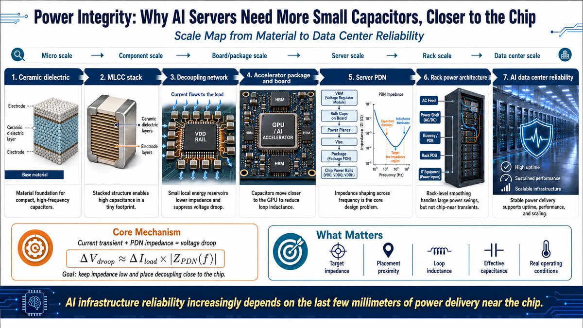
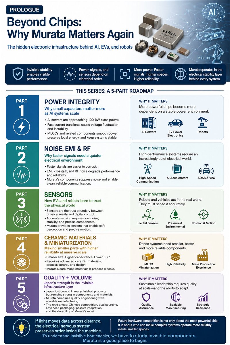
Murata and Japan’s Hidden Electronic Infrastructure
[Part 1. Power Integrity: Why AI Servers Need More Small Capacitors, Closer to the Chip]
Full version: open.substack.com/pub/superp…
The GPU is the chip that does the heavy calculations, but in an AI server the first thing you have to protect is stable voltage. As AI servers get bigger, the power network is no longer just wires. It becomes a system that absorbs sudden power shocks.
When the GPU suddenly pulls a lot of electricity, the system cares more about “keeping the voltage steady” than about raw calculation speed. This is what Power Integrity — power stability — is all about.
1. What matters is not average power, but how fast the power suddenly changes
In AI servers, the real problem is not “how much electricity is used on average.” It is how quickly and sharply the electricity demand changes.
When the GPU starts a big matrix calculation or accesses memory, it pulls a huge burst of current in a very short time. This sudden change causes the voltage to drop for a moment.
If the voltage drops too much, the GPU makes errors or slows down.That is why AI servers need more parts that keep the voltage steady around the GPU.
2. Decoupling capacitors are tiny “electricity reservoirs” right next to the GPU
The main power supply is far away and cannot react instantly when the GPU suddenly needs a lot of current. So engineers place small “electricity reservoirs” right next to the GPU. These are called decoupling capacitors.
When the GPU demands a sudden burst of power, the nearby capacitor quickly supplies electricity and prevents the voltage from dropping. The closer the capacitor is to the GPU, the more stable the voltage stays.
3. Why MLCC (multilayer ceramic capacitors) are so important
The most common capacitor used in AI servers is the MLCC.
It is important for three simple reasons:
It is very small → you can fit many of them on a crowded board
It reacts very fast → perfect for sudden power changes
You can place thousands of them around the GPU
Even though each MLCC is tiny, when you use many together they can quickly supply the electricity the GPU needs. Murata keeps making smaller and better MLCCs specifically for AI servers.
4. Capacitors are moving closer and closer to the GPU
In AI servers, the position of capacitors is changing.
They used to sit far away on the board → then closer to the GPU package → now even inside the package or embedded in the chip.
Why? Because power changes are happening faster and faster. If a capacitor is too far away, electricity takes time to travel and the voltage drops more. So engineers are moving capacitors as close as possible to the GPU.
Murata is also developing silicon capacitors for this exact purpose.
5. Power shocks are solved differently at different layers
Power problems in AI servers do not happen in only one place.
At the whole rack level → big energy storage devices are needed
Right next to the GPU chip → tiny MLCCs and other small capacitors do the job
For example, NVIDIA’s latest AI servers use large storage at the rack level, but still rely heavily on MLCCs right beside each GPU.
The upper layers use higher voltage to send power farther, while the lower layers (near the chip) focus on very low voltage, high current, and ultra-fast changes.
#Murata #MLCC #PowerIntegrity #AIInfrastructure #Decoupling #HiddenAIHardware
3
2
13
1,138
6. Why Murata is becoming more important
Murata is getting attention in the AI era not just because “more MLCCs are used.” The real reason is that the bottleneck in AI servers is moving from the compute chip itself to the power stability layer.
Murata makes MLCCs, inductors, EMI filters, power modules — basically the entire toolkit for keeping power stable. Murata’s own reports clearly state that as AI servers grow, power stability is becoming a critical bottleneck and the demand for their components is rising.
7. What to watch for in the future
When looking at AI server power stability, the important numbers are not just “how many capacitors.”
What really matters is: How close the capacitors are placed to the GPU
How well different types of capacitors work together to keep voltage steady
Whether they still perform well under real conditions (heat, voltage changes, aging)
These points show whether Murata is just a parts supplier or a real design partner in AI servers.
8. What is important — and what is not
Not important:
How many MLCCs are inside one AI server
Whether Murata is simply an “AI beneficiary stock”
Important:
How well the voltage stays steady when the GPU suddenly demands power
How deeply Murata is involved in the overall power stability design
9. Conclusion: The last few millimeters of AI infrastructure
The bottlenecks in AI infrastructure do not stop at the GPU. There is a quieter bottleneck right under the chip — in the last few millimeters — called power integrity.
As AI accelerators become more powerful, the GPU demands more electricity in sudden bursts. What the GPU really needs is not just power — it needs steady, unshakable voltage.
Understanding Murata starts with seeing this invisible “power stability layer.”
3
381
Murata and Japan’s Hidden Electronic Infrastructure
[Part 1. Power Integrity: AI 서버는 왜 작은 콘덴서를 더 많이, 더 가까이 필요로 하는가]
Full version: open.substack.com/pub/superp…
GPU는 계산을 빠르게 하는 칩이지만, AI 서버는 먼저 전압을 안정적으로 유지해야 한다. AI 서버가 커질수록 전원망은 단순한 전선이 아니라, 순간적인 전력 충격을 흡수하는 시스템이 된다.
GPU가 갑자기 많은 전기를 끌어당기는 순간, 시스템은 계산 속도보다 먼저 전압이 흔들리지 않는 것을 요구한다.
이것이 바로 Power Integrity, 즉 전원 안정성 문제다.
1. 중요한 것은 평균 전력이 아니라 전력이 갑자기 변하는 속도
AI 서버에서 진짜 어려운 문제는 평소에 전기를 얼마나 쓰는가가 아니라, 전기가 얼마나 빠르고 급격하게 변하는가다.
GPU는 대규모 계산을 시작하거나 메모리를 접근할 때 순간적으로 엄청난 전류를 끌어당긴다. 이 순간적인 변화가 전압을 순간적으로 떨어뜨린다. 전압이 너무 떨어지면 GPU가 제대로 작동하지 못하고, 오류가 생기거나 성능이 떨어진다.
그래서 AI 서버는 GPU뿐 아니라, GPU가 보는 전원을 안정적으로 만들어주는 부품들이 점점 더 중요해지고 있다.
2. Decoupling capacitor는 GPU 바로 옆에 있는 작은 전기 저장소
전원 공급기는 멀리서 전기를 보내주지만, GPU가 순간적으로 많은 전기를 요구할 때는 반응이 늦다. 그래서 GPU 바로 옆에 작은 전기 저장소 역할을 하는 부품을 둔다. 이 부품이 바로 decoupling capacitor(디커플링 콘덴서)다.
콘덴서는 순간적으로 전기를 빠르게 공급해 전압이 흔들리는 것을 막아준다. 콘덴서를 GPU에 가까이 둘수록 전압이 더 안정적으로 유지된다.
3. 왜 MLCC(적층세라믹콘덴서)가 중요한가
AI 서버에서 가장 많이 쓰이는 콘덴서가 MLCC다.
이유는 간단하다.
작다 (공간이 좁은 AI 보드에 많이 넣을 수 있다)
빠르다 (순간적인 전기 변화에 잘 반응한다)
많이 깔 수 있다 (GPU 주변에 수만 개를 배치할 수 있다)
MLCC 하나하나가 작지만, 여러 개를 함께 쓰면 GPU가 갑자기 전기를 요구할 때 빠르게 대응할 수 있다. Murata는 이 MLCC를 AI 서버용으로 계속 더 작고 더 좋은 성능으로 만들고 있다.
4. 콘덴서는 점점 GPU에 가까워지고 있다
AI 서버에서 콘덴서 위치가 점점 바뀌고 있다.
보드 위 멀리 떨어진 곳 → GPU 패키지 근처 → 패키지 내부 → 심지어 칩 안에까지 들어가고 있다.
이유는 전기 변화가 점점 빠르기 때문이다. 콘덴서가 GPU에서 멀면 전기가 전달되는 동안 시간이 걸리고, 전압이 더 크게 흔들린다. 그래서 콘덴서를 최대한 가까이 붙이는 것이 점점 더 중요해지고 있다.
Murata는 이런 방향으로 실리콘 콘덴서 같은 제품도 개발하고 있다.
5. 전력 충격은 계층마다 다르게 해결된다
AI 서버의 전력 문제는 한 곳에서만 생기지 않는다.
랙 전체 수준에서는 큰 전력 저장 장치가 필요하다
GPU 칩 바로 근처에서는 작은 MLCC와 콘덴서가 필요하다
NVIDIA의 최신 AI 서버도 랙 수준에서는 큰 저장 장치를 쓰지만, 칩 근처에서는 MLCC가 핵심 역할을 한다.
상위 계층은 고전압으로 전기를 멀리 보내고, 하위 계층은 낮은 전압에서 빠른 변화를 안정시키는 식이다.
#Murata #MLCC #PowerIntegrity #AIInfrastructure #Decoupling #HiddenAIHardware
1
5
23
1,859
6. Murata가 주목받는 이유
Murata가 AI 시대에 다시 중요해지는 이유는 MLCC가 더 많이 들어가서가 아니다. AI 서버의 병목이 단순한 계산 칩에서 전원 안정성 계층으로 이동하고 있기 때문이다.
Murata는 MLCC뿐 아니라 콘덴서, 인덕터, EMI 필터, 전원 모듈까지 전원 안정성 전체를 다루는 회사다. Murata 자료에서도 AI 서버가 커질수록 전원 안정성이 핵심 병목이 되고, 이를 해결하는 부품 수요가 늘어난다고 나온다.
7. 앞으로 무엇을 봐야 할까
AI 서버 전원 안정성을 볼 때 중요한 것은 단순한 숫자가 아니다.
콘덴서가 GPU에 얼마나 가까이 붙어 있는가
여러 종류의 콘덴서를 잘 조합해 전압을 안정적으로 유지하는가
실제 사용하는 환경(온도, 전압)에서도 제대로 작동하는가
이런 부분을 봐야 Murata가 단순한 부품 공급자가 아니라, AI 서버 설계의 중요한 파트너인지 알 수 있다.
8. 중요한 것과 중요하지 않은 것
중요하지 않은 것:
AI 서버 한 대에 MLCC가 몇 개 들어가는가
Murata가 단순히 AI 수혜주인가
중요한 것:
GPU가 순간적으로 전기를 요구할 때 전압이 얼마나 잘 버티는가
Murata가 전원 안정성 전체 설계에서 얼마나 깊이 들어가는가
9. 결론: AI 인프라의 마지막 몇 밀리미터
AI 인프라의 병목은 GPU에서 끝나지 않는다.
칩 바로 아래, 마지막 몇 밀리미터에서 전원 안정성 문제가 점점 커지고 있다. AI accelerator가 더 강해질수록 GPU는 더 많은 전기를 순간적으로 요구한다. 그때 GPU가 원하는 것은 단순한 전력이 아니라 흔들리지 않는 안정적인 전압이다.
Murata를 이해하는 첫걸음은 바로 이 보이지 않는 전원 안정성 계층을 보는 것이다.
8
479
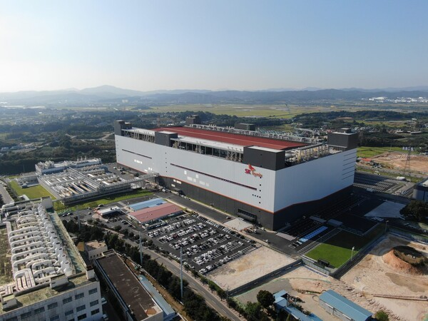
SK HYNIX SELECTS TOKYO ELECTRON EQUIPMENT FOR 375-LAYER NAND DEPOSITION
SK Hynix to Mass-Produce Next-Generation 375-Layer 3D NAND by Year-End
SK Hynix will begin mass production of its next-generation 375-layer 3D NAND flash at the end of this year.
According to industry sources on the 11th, SK Hynix has completed production qualification of the 375-layer NAND and is preparing to transfer it to mass production lines. This is not a new fab expansion. Instead, a conversion investment is underway to switch existing production lines at the M15 fab in Cheongju (which currently produce 176-, 238-, and 321-layer products) over to the 375-layer product.
The 375-layer product was originally discussed as a 400-layer-class device. The layer count was lowered to 375 due to the high difficulty of mass-producing high-stack processes. As NAND layer counts rise, the difficulty of processes such as channel hole etching increases. An industry official said, "The product formerly referred to as 400-layer class has been revised to 375 layers," adding, "The roadmap from there leads to 480 layers and then 604 layers."
The key change is the adoption of molybdenum (Mo). Part of the tungsten (W) film used previously has been replaced with molybdenum. NAND increases capacity by vertically stacking hundreds of layers of charge-storing cells and the word lines that control them. At 375 layers, SK Hynix decided to switch part of the word line material — the metal gate electrodes controlling each cell layer — from tungsten to molybdenum.
Molybdenum is regarded as a material that can overcome tungsten's limitations in high-stack NAND. As layer counts increase, interconnects become thinner, and tungsten's electrical resistance rises as it scales down, slowing signal transmission. Molybdenum can achieve lower resistance than tungsten in miniaturized word line structures, delivering signals faster — meaning faster program and erase speeds. In particular, tungsten requires a barrier liner to be deposited before the fill, and since this liner is laid down at every layer, it causes thickness loss. Molybdenum can be filled directly without a barrier layer, enabling higher density.
The process difficulty is high, however. Molybdenum precursors are solid at room temperature, requiring technology to heat them to high temperatures and deliver them at a consistent volume and rate.
Samsung Electronics already applied molybdenum to its metal interconnect process starting with its 9th-generation 286-layer 3D NAND, which entered mass production in April 2024. Its next-generation 10th-gen 3D NAND exceeds 400 layers and is being prepared for commercialization in the second half of this year, with molybdenum applied to a larger number of process steps.
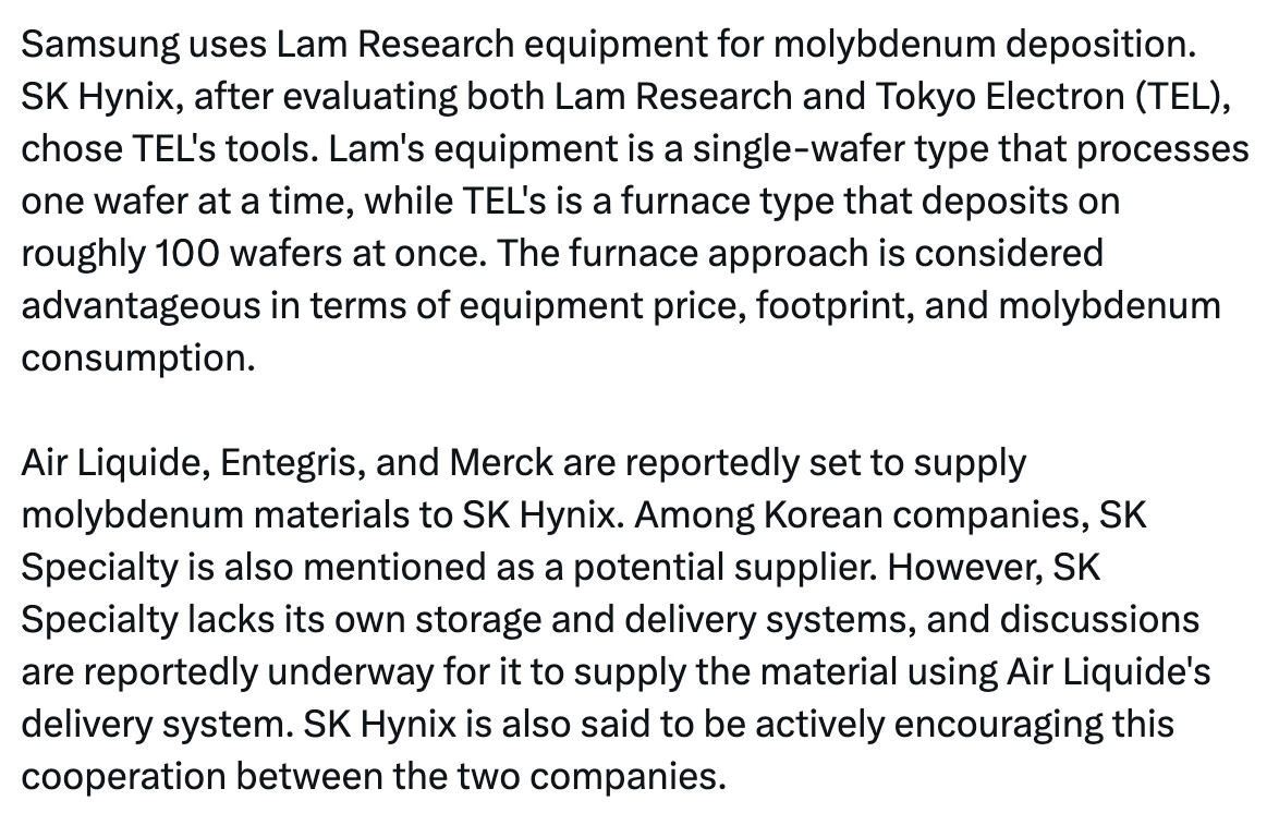
Samsung uses Lam Research equipment for molybdenum deposition. SK Hynix, after evaluating both Lam Research and Tokyo Electron (TEL), chose TEL's tools. Lam's equipment is a single-wafer type that processes one wafer at a time, while TEL's is a furnace type that deposits on roughly 100 wafers at once. The furnace approach is considered advantageous in terms of equipment price, footprint, and molybdenum consumption.
Air Liquide, Entegris, and Merck are reportedly set to supply molybdenum materials to SK Hynix. Among Korean companies, SK Specialty is also mentioned as a potential supplier. However, SK Specialty lacks its own storage and delivery systems, and discussions are reportedly underway for it to supply the material using Air Liquide's delivery system. SK Hynix is also said to be actively encouraging this cooperation between the two companies.
Molybdenum consumption for 3D NAND is expected to grow rapidly. The industry estimates that Samsung purchased around 4 tons last year and will purchase around 10 tons this year, rising to 25 tons in 2027, 40 tons in 2028, 60 tons in 2029, and 80 tons by 2030. SK Hynix, which begins using molybdenum in earnest next year, is estimated to start at around 4 tons per year.
Another industry official explained, "Unlike DRAM, the NAND industry still operates on profitability rather than volume," adding, "SK Hynix, likewise, has chosen the path of cutting output of older, lower-layer-count NAND and ramping 375-layer production to raise bit productivity and lower costs, rather than adding new capacity."
12
39
469
145,918
슈포 (Superposition) retweeted

Jun 10
고장난 국장 😵
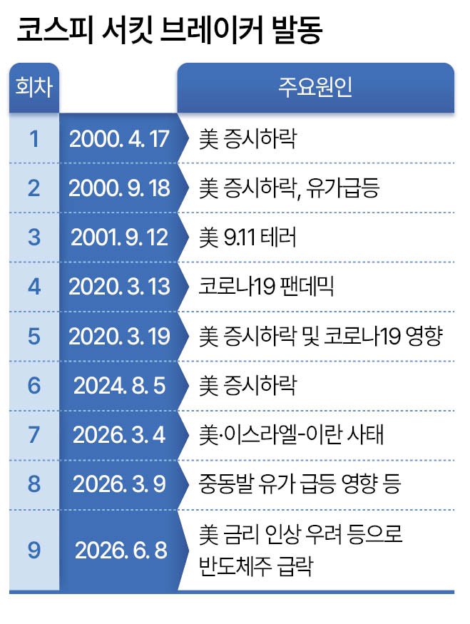
1. 올해 코스피 시장에서 서킷브레이커 3차례 발동.
2. 거래소 통계상 코스피 시장에서 발동된 서킷브레이커는 총 9차례인데, 그중 3차례가 올해에 집중.
3.사이드카는 올해 벌써 총 23차례 발생. (매수사이드카 12번, 매도사이드카 11번)
4. 올해 1월 부터 6월 9일 기준, 단순 계산하면 일주일에 한 번꼴.
5. 2008년 금융위기 당시 연간기록이 26회였음.
Source: n.news.naver.com/mnews/artic…
9
11
37
8,190