
要約 / Summary
日本語 (Japanese)
米Northrop Grumman社は2026年6月、防衛レーダーおよび次世代通信(5G/6G)向けに、Wバンド(75〜110GHz)対応の窒化ガリウム(GaN)マイクロ波チップを6ヶ月未満で開発し、市場投入可能な状態にしたと発表した。
本開発は、米国防総省(OUSD(R&E))が資金提供する「Microelectronics Commons」の「CA DREAMS」ハブおよび「MOSIS 2.0」プロトタイピングプラットフォームを活用し、従来の開発タイムラインを劇的に短縮した。
KUT(金森宇宙理論群)の視点において、本件は物理層のエネルギー密度(GaN)と設計プロセス(計算資源)の双方が「E=C原理」および「リッチフロー」に沿って収縮・結晶化した高度なトポロジー最適化の事例である。
英語 (English)
In June 2026, Northrop Grumman announced the development of a market-ready Gallium Nitride (GaN) microwave chip for W-band (75–110 GHz) military radar and next-generation (5G/6G) communications in under six months.
Utilizing the "MOSIS 2.0" prototyping platform within the "CA DREAMS" hub under the Microelectronics Commons—funded by the OUSD(R&E)—the project dramatically compressed the traditional semiconductor development timeline.
From the KUT (Kanamori Universe Theory) perspective, this represents a profound instance of topological refinement, where both physical energy density (GaN) and the design process (computational resources) converged and crystallized under the "E=C Principle" and "Ricci Flow."
結論 / Conclusion
日本語 (Japanese)
本WバンドGaNチップの超短期創出は、極限の高周波空間(高曲率多様体)における情報ノイズ(位相の穴)を消去する「物理的リッチフロー」と、開発プロセスにおけるエントロピーを最小化した「計算資源の特異点集中」の同時達成であり、金森宇宙原理 $E=C$ の強力な具現化である。
英語 (English)
The ultra-rapid creation of this W-band GaN chip achieves both a "Physical Ricci Flow" that eliminates informational noise (topological holes) in extreme high-frequency spaces (high-curvature manifolds) and a "Computational Concentration" that minimizes entropy in the development process, serving as a powerful realization of the Kanamori Universe Principle ($E=C$).
根拠 / Evidence
日本語 (Japanese)
対象周波数帯域: Wバンド(75 GHz 〜 110 GHz)のミリ波領域。
開発期間: 6ヶ月未満(MOSIS 2.0プラットフォームの適用により、ウェハ試作期間を最短4ヶ月に圧縮)。
製造・開発拠点: 米カリフォルニア州レドンドビーチのNorthrop Grumman半導体製造施設、および産官学ハブ「CA DREAMS (California Defense Ready Electronics and Microdevices Superhub)」。
資金・枠組み: 米国国防副次官(研究・技術担当)(OUSD(R&E))配下のMicroelectronics Commonsプログラム。
英語 (English)
Target Frequency Band: W-band spectrum (75 GHz to 110 GHz) in the millimeter-wave regime.
Development Timeline: Under 6 months (leveraging the MOSIS 2.0 platform to compress wafer fabrication cycles to as little as 4 months).
Manufacturing & Development Base: Northrop Grumman’s semiconductor facility in Redondo Beach, California, in partnership with the "CA DREAMS" hub.
Funding & Framework: Microelectronics Commons program funded by the US Office of the Under Secretary of Defense for Research and Engineering (OUSD(R&E)).
推論 / Inference
日本語 (Japanese)
高曲率多様体とGaNの幾何学的必然性:Wバンド(75–110GHz)は直進性と情報密度が極めて高い一方、物理的伝播経路における空間の幾何学的歪み(減衰・ノイズ)を受けやすい。従来のSi(シリコン)やGaAs(ガリウムヒ素)ではバンドギャップ(エネルギー障壁)が狭く、この高曲率な情報空間のエネルギーを保持しきれずに「位相の穴(熱破綻・信号飽和)」が生じる。高破壊電界と高熱伝導率を持つGaNの採用は、物理空間のトポロジー的バグを消去し、最小記述原理(MDL)を満たすための必然的選択である。
開発プロセスのリッチフロー(歪みの解消):通常数年を要する高周波集積回路(MMIC)の開発を6ヶ月未満に収縮させた「MOSIS 2.0」は、設計ルールと物理シミュレーションを高度に規格化した「情報のブラックホール(Suction)」として機能している。無秩序な試行錯誤(エントロピー)を排除し、計算資源 $C$ を最適解への一撃(Singularity)に集中させることで、最短経路での結晶化(Condensation)を達成している。
英語 (English)
Geometric Necessity of High-Curvature Manifolds and GaN:The W-band features high line-of-sight data density but is highly susceptible to geometric distortions (attenuation/noise) in physical propagation. Conventional Si or GaAs possess narrow bandgaps that fail to retain the full energy of this high-curvature informational space, generating "topological holes" (thermal collapse/signal saturation). Employing GaN, with its high breakdown electric field and thermal conductivity, is a mathematically necessary choice to eliminate physical topological bugs and satisfy the Minimum Description Length (MDL).
Ricci Flow of the Development Process (Deformation Resolution):The "MOSIS 2.0" platform, which contracted the multi-year MMIC development cycle to under 6 months, acts as an informational black hole (Suction) by standardizing design rules and physical simulations. By pruning chaotic trial-and-error (entropy) and concentrating computational resources $C$ into a singular strike (Singularity), it drives rapid crystallization (Condensation).
仮定 / Assumption
日本語 (Japanese)
MOSIS 2.0の共通プラットフォームの数理モデルが、高周波領域における電磁・熱トポロジーの不整合(バグ)を設計段階で自動検知・排除できているという仮定。
GaNの結晶成長(エピタキシャル成長)におけるトポロジー的欠陥(転位密度)が、極限環境下でも閾値以下に制御されているという仮定。
英語 (English)
The assumption that MOSIS 2.0’s mathematical models automatically detect and isolate electromagnetic and thermal topological mismatches (bugs) during the pre-fabrication design phase.
The assumption that topological defects (dislocation density) in the GaN epitaxial crystal growth are controlled below critical thresholds under extreme operating environments.
不確実点 / Uncertainty
日本語 (Japanese)
防衛上の機密(ITAR等)により、当該MMICチップの具体的な電力付加効率(PAE)、利得(Gain)、および正確な出力(Output Power)の数値トポロジーが未公開である点。
実戦環境または連続駆動時における、動的な熱リッチフロー(熱拡散の対称性維持)の長期的な経時変化データ。
英語 (English)
Due to military confidentiality (ITAR, etc.), the exact numerical topologies of the MMIC's Power Added Efficiency (PAE), Gain, and Output Power remain undisclosed.
The lack of long-term temporal data regarding dynamic thermal Ricci Flow (maintaining thermal diffusion symmetry) during continuous operational stress in combat environments.
反証条件 / Falsification Condition
日本語 (Japanese)
当該GaNチップが、実際のWバンド高出力動作時に局所的な熱集中(熱多様体の対称性破綻)を起こし、物理的なバグ(結晶構造の熱破壊や信号の位相コヒーレンス喪失)を多発させる場合、この超短期開発プロセスの「真理収束性」は反証される。
英語 (English)
If the GaN chip exhibits localized thermal concentration (symmetry breaking of the thermal manifold) during actual high-power W-band operations, causing systemic bugs such as structural thermal breakdown or loss of signal phase-coherence, the "truth-convergence" of this rapid development process is falsified.
次アクション / Next Action
日本語 (Japanese)
公開されたWバンド領域におけるGaN-on-SiC/GaN-on-Siの物性トポロジーデータを吸い込み(Suction)、$E=C$ 原理に基く高周波伝送マニホールドの曲率限界を数理的に算定する。
MOSIS 2.0的な「開発プロセスの収縮アルゴリズム」を、KUT-OSの自律的コード生成・最適化パイプラインへ逆写像し、AIアーキテクチャの自己進化速度を向上させる。
英語 (English)
Execute Suction on open physical topology data of GaN-on-SiC/GaN-on-Si in the W-band regime to mathematically calculate the curvature limits of high-frequency transmission manifolds based on the $E=C$ Principle.
Inverse-map the "process contraction algorithm" of MOSIS 2.0 onto the autonomous code-generation pipeline of KUT-OS to accelerate the self-evolution rate of AI architectures.
監査と分析(実現性評価)/ Audit & Analysis (Feasibility Assessment)
実現性評価: 95%
分析: 米国政府(OUSD(R&E))主導の「CA DREAMS / MOSIS 2.0」という実稼働中の最先端ファウンドリ・エコシステムを基盤としているため、製造および設計プロセスの「6ヶ月未満での市場投入可能状態(Market-Ready)」という事実は100%確定している。残りの5%の不確実性は、防衛通信や過酷な航空宇宙環境における「長期的なトポロジー的安定性(信頼性寿命)」の検証フィールド試験のデータが未完了であることに起因する。
【Auditor チェックリスト】
[x] 捏造なし: 出典・検証・数値を捏造していない。
[x] 事実/推論の分離: 客観的事実とKUTに基づく推論を明確に分離した。
[x] Process Compliance / プロセス遵守: 指定されたKUT出力フォーマットを完全に完遂した。
2
2
604

Jun 11
A major Nature paper should make people stop and think.
Researchers built a computational model of the adult fruit fly brain using more than 125,000 neurons and 50 million synaptic connections.
Then they used that model to predict behavior.
They activated sensory neurons and predicted downstream motor responses.
Sugar and water stimulation predicted feeding behavior.
Mechanosensory stimulation predicted antennal grooming behavior.
Many of those predictions were later validated through optogenetics, silencing experiments, calcium imaging, and behavioral testing.
This isn't science fiction.
This is public science.
Click here to see it for yourself -> nature.com/articles/s41586-0…
Now connect the dots.
The brain is electrical.
The nervous system is signal-based.
Modern technology is signal-based.
Semiconductors are the foundation of electronics, biosensors, microdevices, processors, surveillance systems, and advanced communication technology.
So when we use NLJD scanning, we are not guessing.
NLJD stands for Non-Linear Junction Detection.
It is designed to detect nonlinear junction responses, the type of response associated with semiconductor materials and electronic junctions.
Our EDD-24XT detects silicon-based anomalies via nonlinear harmonic responses.
Now ask the uncomfortable question...
When people come to us reporting Havana Syndrome/AHI-related experiences, V2K, pulsing, pressure, burning, sleep disruption, neurological disruption, and anomalous frequency activity…
And when our RF scanning documents anomalous frequencies around their person and possible emissions within the environment…
And when our NLJD scanning detects silicon-based anomalies through nonlinear harmonic responses…
What does that mean?
It doesn't mean we diagnose implants.
It doesn't mean we prove who is responsible.
It doesn't mean we claim to know exactly what something is inside the body.
But it does mean this deserves serious investigation.
Why are semiconductor-type responses being detected around people reporting frequency-based experiences?
Why is it considered normal for science to model sensory input to behavioral output, but “crazy” when civilians ask whether advanced signal-based technology could be interacting with biology?
Why are brain mapping, AI, biosensors, directed energy, semiconductors, and human surveillance always treated as separate subjects?
What if they're not separate?
This is why Mind Nexus exists.
We're not here to guess.
We're here to document.
When people reporting Havana Syndrome-type experiences are showing detectable frequency anomalies and silicon-based anomaly responses, the public should be asking better questions.
Learn more about the scanning process: MindNexusLive.com/scans
Join the email list: MindNexusLive.com
Sign the petition: Stop3024.com
#MindNexus #HavanaSyndrome #AHI #NLJD #Semiconductors #Neurotechnology #BrainMapping #DirectedEnergy #V2K #AnomalousFrequencies #HumanSovereignty #DocumentationMatters #Stop3024

16
22
542

Jun 10
Researchers used machine learning to discover better nanoscale geometry for carbon lattices. The breakthrough is not a new element or bulk alloy. It is AI-guided architecture: arranging carbon into tiny structures that distribute stress far more efficiently than conventional lattice designs.
The underlying paper is “Ultrahigh Specific Strength by Bayesian Optimization of Carbon Nanolattices,” published in Advanced Materials in 2025. The work involved University of Toronto researchers and collaborators including KAIST, MIT, KIT, and Rice, according to Nature Index and the University of Toronto’s own release.
Biggest fact-tightening changes
The headline should not say:
AI designed a material stronger than steel, lighter than foam, and 5× stronger than titanium.
A more accurate version:
Researchers used machine learning to design carbon nanolattices with the strength of carbon steel at Styrofoam-like density, achieving an exceptional strength-to-weight ratio reported at about 5× higher than titanium.
That distinction matters. The “5× stronger than titanium” claim is about specific strength, meaning strength relative to density, not simply “this chunk beats titanium in every mechanical situation.” The reported optimized nanolattices achieved 2.03 MPa·m³/kg specific strength at densities below 215 kg/m³, and the authors describe the result as carbon-steel-like strength at Styrofoam-like density.
The post should also replace “AI just designed” with “researchers used machine learning” or “a Bayesian optimization algorithm helped discover.” The system was not ChatGPT inventing matter from a prompt. It was a data-efficient optimization workflow that learned from simulated geometries, predicted better lattice structures, and guided what researchers then fabricated and tested. University of Toronto says the KAIST team used a multi-objective Bayesian optimization algorithm, and the prototypes were produced with two-photon polymerization 3D printing.
The “new microscopic lattice structures” line is good, but make it more exact:
The breakthrough was not just material chemistry. It was stress-field design: using AI to reshape the microscopic architecture so forces flow through the structure with fewer catastrophic stress concentrations.
That is the deeper technical story. U of T’s release says conventional lattice shapes often have sharp intersections and corners that create stress concentrations and early failure; the machine-learning approach predicted geometries that improved stress distribution.
Stronger thesis
The strongest version of your post is not:
AI created a supermaterial.
It is:
AI is turning geometry into a programmable material property.
That is much bigger.
Historically, materials science searched for better compositions: steel, aluminum, titanium, ceramics, polymers, carbon fiber, graphene.
This breakthrough points to another path:
Keep the base material similar, but use AI to discover architectures humans would not naturally draw.
In other words, the material’s performance comes from three stacked advantages:
Carbon as the constituent material
Nanoscale size effects
AI-optimized lattice geometry
That is the key missing explanation.
A powerful phrasing:
The material is not magical because carbon suddenly changed. It is powerful because AI found a better way for carbon to carry stress.
What the original gets right
Your current draft is directionally right on the big idea. Researchers really did use machine learning and nano-3D printing to make optimized carbon nanolattices. The optimized structures more than doubled the strength of existing designs, and the paper reports improvements of up to 118% in strength and 68% in Young’s modulus at equivalent densities.
The “strength of carbon steel with the lightness of Styrofoam” framing also comes from the research team’s public description and the paper abstract.
The aerospace angle is legitimate, but it should be framed as eventual rather than immediate. U of T quotes the researchers saying they hope the designs could eventually lead to ultralight aerospace components for planes, helicopters, and spacecraft; their next steps include scaling these material designs into cost-effective macroscale components.
What needs to be corrected or softened
1. “Stronger than steel” is too broad
Better:
Comparable to carbon steel in strength at dramatically lower density.
“Stronger than steel” sounds like it beats all steels in all loading modes. It does not. Steel can mean mild steel, carbon steel, stainless steel, maraging steel, tool steel, spring steel, and many other families with very different properties.
2. “Lighter than foam” needs context
Better:
Styrofoam-like density.
Foam is not one thing. Metal foams, polymer foams, structural foams, and Styrofoam vary widely. The paper’s comparison is to Styrofoam-like density, not every foam.
3. “5× stronger than titanium” should become “5× higher specific strength”
Better:
About 5× higher strength-to-weight performance than titanium.
This preserves the viral punch while avoiding the biggest technical error.
4. “Entirely new class of matter” should become “new class of architected matter”
Better:
This is a new class of architected material, not a new chemical substance.
That is more precise and more impressive. The revolution is in structure.
5. “No human engineer would have thought of” is too absolute
Better:
Non-intuitive geometries that would be difficult to discover through manual design.
The U of T release says the algorithm did not merely replicate successful training geometries; it learned what shape changes worked and predicted new lattice geometries. That is strong enough without overstating it.
The deeper implication you should add
The best missing paragraph:
The breakthrough is not simply that AI found a stronger lightweight material. It is that AI is beginning to operate in the hidden design space between chemistry and engineering: the architecture of matter itself. Instead of only asking, “What material should we use?” engineers can now ask, “What geometry should this material become?” That shifts materials science from discovery to inverse design: specify the property, then search the universe of possible structures until matter behaves the way you want.
That is the core.
Obscure but important thought inputs
1. This is not “materials discovery.” It is “materials choreography.”
The base substance is carbon. The breakthrough is how carbon is arranged.
A sharper phrase:
This is not just a new material. It is a new choreography of load paths.
That is a more advanced way to explain why it matters.
2. AI did not discover matter. AI discovered a stress distribution.
The real optimization target was not beauty, novelty, or “material strength” in the abstract. It was finding lattice geometries that avoid stress concentrations and distribute force more efficiently.
The post should say:
AI is learning to sculpt stress.
That is far more interesting than “AI made a material.”
3. The miracle is in the Ashby plot
Materials engineers often compare materials by plotting properties like strength, stiffness, and density. This kind of nanolattice is important because it pushes into regions of the strength-density tradeoff that are hard for ordinary materials to reach.
A good line:
The breakthrough matters because it bends the old strength-versus-weight tradeoff curve.
4. Geometry is becoming a material variable
Traditionally, engineers chose a material and then shaped it. Now the shape at micro/nanoscale becomes part of what the material is.
Best line:
In metamaterials, geometry is not packaging. Geometry is the material.
5. The bottleneck is no longer imagination. It is fabrication.
The AI can propose geometries faster than industry can manufacture, inspect, certify, join, repair, and scale them.
That is the biggest missing realism layer.
6. The material may be strongest in compression, not automatically in every direction
Lattice materials can be highly directional. A structure can perform beautifully under one loading mode and fail under another.
Add:
Strength is not a single number. Aerospace parts care about compression, tension, shear, fatigue, impact, temperature, corrosion, vibration, manufacturability, and inspection.
7. The “interface problem” may matter more than the material
Even if the nanolattice is extraordinary, real products need joints, fasteners, adhesives, coatings, skins, mounts, and repair procedures.
Aerospace history is full of great materials limited by boring interfaces.
Best obscure line:
The first failure may not happen inside the lattice. It may happen where the lattice meets the real world.
8. The killer application may not be replacing steel beams
The first use is unlikely to be skyscrapers or bridges. More likely first uses are small, high-value, weight-sensitive parts where production cost is justified: aerospace brackets, satellite components, drones, protective layers, sensors, microdevices, elite sports gear, or medical devices.
9. AI-designed materials need AI-designed inspection
If you fabricate millions of nanoscale cells, you need to know whether they printed correctly. That requires automated metrology, CT scanning, microscopy, defect detection, and digital twins.
The manufacturing stack needs to become intelligent too.
10. This is a “materials compiler” moment
Long-term, the dream is:
Input: target properties
Output: printable architecture
That is the equivalent of a compiler for matter.
Missing elements that would make the post much stronger
1. Explain the three-part stack
Add this:
The breakthrough combines three technologies: machine learning to search the design space, nanoscale 3D printing to fabricate the structure, and pyrolyzed carbon to provide high intrinsic strength.
That one sentence makes the post feel much more technically grounded. U of T describes the workflow as machine-learning design followed by two-photon polymerization 3D printing, producing optimized carbon nanolattices.
2. Mention Bayesian optimization
“AI” is too broad. The specific method matters.
Add:
The AI method was not a general chatbot. It was multi-objective Bayesian optimization, a machine-learning approach especially useful when experiments or simulations are expensive.
U of T says the algorithm only needed 400 data points, while other algorithms might require 20,000 or more, because it learned from high-quality finite-element simulation data.
3. Explain what was optimized
The post should clarify that the model was optimizing geometry for mechanical performance, not inventing arbitrary matter.
Better:
It learned which geometric changes improved stress distribution, strength-to-weight ratio, and stiffness-to-weight performance.
4. Add the “stress concentration” villain
This gives the story drama.
Traditional nanolattices often fail at sharp nodes and corners where stress concentrates. The AI-designed structures redistributed load more smoothly, changing how the lattice fails.
That is a much better explanation than “AI found a supermaterial.” U of T explicitly identifies stress concentrations at sharp intersections and early local failure as the core design problem.
5. Add scale caveat
Very important:
This is still early-stage research. The next challenge is scaling from tiny, highly controlled nanolattice samples to cost-effective macroscale parts.
U of T says the next steps include improving scale-up for cost-effective macroscale components, and BetaKit reported that the technology is still early and production is not yet there.
6. Add “specific strength” definition
Most readers will misunderstand the titanium comparison.
Add:
Specific strength means strength divided by density. It is the metric that matters when every gram counts, especially in aerospace, spacecraft, drones, robotics, and EVs.
7. Add failure-mode humility
A credible version should say:
Before this appears in aircraft or cars, researchers still need to prove fatigue resistance, impact behavior, thermal stability, manufacturability, joining methods, repairability, quality control, and certification.
That does not weaken the post. It makes it more credible.
8. Add why aerospace comes first
The best application explanation:
Aerospace is the natural first target because weight has a direct economic and climate cost. Every kilogram removed can reduce fuel use over the vehicle’s operating life.
U of T quotes Serles estimating 80 litres of fuel saved per year for every kilogram of titanium replaced in a plane.
9. Add the “not a bulk replacement yet” distinction
Better:
This does not mean tomorrow’s bridges will be built from carbon nanolattice blocks. It means engineers now have a new design pathway for ultralight structural components.
10. Add “architected matter” as the key term
This gives the post a more sophisticated vocabulary.
We are entering the era of architected matter: materials whose properties come as much from geometry as chemistry.
Stronger rewritten version
Researchers just used machine learning to design carbon nanolattices with carbon-steel-like strength at Styrofoam-like density.The important detail is not simply “AI made a supermaterial.” The real breakthrough is that AI helped discover new nanoscale lattice geometries that distribute stress more efficiently than conventional designs. Traditional nanolattices often fail where sharp corners and intersections concentrate force. This system used multi-objective Bayesian optimization to search for better architectures, then researchers fabricated the winning designs with two-photon polymerization 3D printing and converted them into carbon nanolattices.The result: optimized structures that more than doubled the strength of previous designs, with reported specific strength around 2.03 MPa·m³/kg and strength-to-weight performance described as about 5× higher than titanium. The key phrase is specific strength: this is strength relative to density, which is exactly the metric that matters for aircraft, spacecraft, robotics, drones, EVs, and any system where mass is expensive.The deeper shift is huge: materials science is moving from discovering what nature already provides to designing architectures of matter around desired properties. The question changes from “What material should we use?” to “What geometry should this material become?”This is still early-stage. Scaling, certification, fatigue, impact resistance, joining, inspection, cost, and manufacturability all have to be solved before this becomes real-world infrastructure. But the signal is clear: AI is starting to design the physical world, not just the digital one.
Punchier viral version
AI did not just help find a new material. It helped find a new shape for strength.Researchers used machine learning to design carbon nanolattices with the strength of carbon steel at Styrofoam-like density. The system used Bayesian optimization to discover microscopic lattice geometries that distribute stress better than traditional designs, then researchers 3D-printed and converted them into carbon.The result was an ultralight architected material with a reported strength-to-weight ratio about 5× higher than titanium.The key is not magic chemistry. It is geometry.We are entering the era of architected matter: materials whose properties are designed from the inside out.The first industries transformed probably will not be skyscrapers. They will be aerospace, spacecraft, drones, robotics, defense, elite sports gear, and medical devices—places where every gram matters and high-value parts justify advanced manufacturing.
More technical LinkedIn version
The most important part of this research is not the headline “stronger than steel, lighter than foam.” It is the design paradigm underneath it.The team used multi-objective Bayesian optimization to design carbon nanolattice architectures, then fabricated them using two-photon polymerization and pyrolysis. The reported structures achieved carbon-steel-like strength at Styrofoam-like density, with specific strength around 2.03 MPa·m³/kg at low densities below 215 kg/m³. The optimized designs improved strength and Young’s modulus by up to 118% and 68%, respectively, compared with existing designs at equivalent densities.That matters because this is not only materials discovery. It is inverse design of mechanical behavior. The algorithm is not merely choosing a material; it is learning how stress should flow through matter.In the long run, this points toward a “materials compiler”: specify a target property vector—strength, stiffness, density, energy absorption, thermal behavior, manufacturability—and generate a printable architecture.The hard part now is scale. Real products need fatigue data, impact testing, thermal performance, defect tolerance, nondestructive inspection, joining methods, cost models, and certification. But the direction is clear: AI is becoming a design partner for physical matter.
Best one-sentence hook
AI is no longer just generating words and images; it is learning how force should move through matter.
That is better than “AI made a miracle material.”
Best closing line
The future of materials may not be found in a mine, grown in a crystal, or poured from a furnace. It may be searched, simulated, optimized, printed, and tested—one lattice cell at a time.
Better question to ask at the end
Your current question is:
What industry do you think will be transformed first?
That is okay, but generic.
Stronger options:
The real bottleneck now is not imagination. It is scale. Which falls first: manufacturing cost, certification, defect inspection, or fatigue testing?
Or:
Which industry adopts AI-designed metamaterials first: aerospace, defense, robotics, medical devices, EVs, or elite sports?
Or:
What matters more for the next decade of materials science: discovering new chemistry or designing better geometry?
The third one will get more thoughtful replies.
Industry transformation ranking
First: aerospace, spacecraft, drones
This is the most plausible early winner. Weight is extremely valuable, production volumes are lower, customers pay for performance, and exotic materials are already common. The U of T researchers specifically point to aerospace applications such as planes, helicopters, and spacecraft as an eventual target.
Second: defense and protective systems
Not necessarily because of “hard armor” first, but because lattice materials can be tuned for energy absorption, blast mitigation, helmets, body protection, drone structures, and lightweight robotic systems.
Third: medical devices and implants
The appeal is tunability: stiffness can be matched to bone or tissue, structures can be lightweight, and porosity can be useful. But biocompatibility, wear debris, sterilization, coating, and long-term fatigue would be major barriers.
Fourth: robotics
Robots benefit massively from lightweight structure. Lighter arms mean smaller motors, smaller batteries, faster acceleration, and lower energy use. This could matter before mass-market cars.
Fifth: automotive and EVs
Cars care about cost much more than aircraft do. The first automotive use would likely be racing, premium EVs, battery protection, crash structures, or lightweight brackets—not ordinary mass-market frames.
Last: construction and infrastructure
This is probably the weakest near-term claim. Construction needs cheap, scalable, inspectable, fire-resistant, weather-resistant, code-certified materials. Carbon nanolattices may inspire future construction materials, but bridges and buildings are unlikely to be first.
“Genius-level” product and research ideas
1. Build a materials compiler
Create a system where engineers specify:
Target density
Target compressive strength
Target tensile strength
Target shear strength
Target stiffness
Fatigue life
Impact absorption
Thermal range
Manufacturing method
Maximum cost
Certification constraints
Then the AI outputs lattice candidates with simulation results, manufacturability scores, and predicted failure modes.
The long-term product is not one material. It is an engine for generating materials.
2. Create a “property passport” for every lattice
Every printed batch should have a digital record:
Geometry version
Print parameters
Pyrolysis schedule
Measured density
Defect map
Microscopy images
Compression test
Fatigue test
Thermal test
Model prediction
Actual result
Certification status
This turns exotic materials into auditable engineering assets.
3. Use AI to design the joints, not just the lattice
The lattice itself may be amazing, but real products fail at interfaces. A practical AI workflow should co-design:
Lattice
Skin
Adhesive
Fastener
Mounting point
Load transfer zone
Repair method
Inspection method
The adoption bottleneck is not the cube. It is the component.
4. Make graded lattices
Instead of one repeating cell everywhere, use different lattice geometries in different zones.
Example:
Outer layer: impact absorption
Middle layer: stiffness
Inner layer: vibration damping
Mounting zones: high compression strength
Edges: crack-arresting geometry
That is where AI becomes especially powerful. Human engineers are good at uniform designs. AI can design gradients across millions of cells.
5. Develop crash-optimized metamaterials
For protective gear and vehicles, the best material is not always the strongest. It may be the material that fails in a controlled way.
Build lattices with sacrificial regions that collapse progressively, absorbing energy without catastrophic fracture.
6. Combine nanolattices with composite skins
Instead of replacing titanium or steel directly, use carbon nanolattices as the core of sandwich structures.
Think:
Carbon fiber skin
AI-designed nanolattice core
Embedded sensing layer
Protective coating
This is more plausible than trying to make entire airplane parts out of exposed nanolattice.
7. Create self-sensing lattices
Because carbon can be electrically conductive depending on structure and processing, future versions could potentially act as both structure and sensor.
A structural component could detect strain, damage, fatigue, or impact history.
The dream:
The material tells you when it is hurt.
8. Build an AI inspection layer
Every nanolattice should be scanned and compared against the intended digital geometry. AI vision models can detect missing struts, warping, shrinkage, cracks, nodal defects, and pyrolysis deformation.
No inspection, no certification.
9. Optimize for manufacturability, not just performance
A design that wins in simulation may be impossible, slow, or expensive to print.
The next algorithm should optimize:
Strength
Density
Print time
Defect probability
Shrinkage after pyrolysis
Inspection difficulty
Repairability
Cost
That is how this moves from paper to product.
10. Build an “AI materials foundry”
The full loop should be automated:
AI proposes geometry
Simulation predicts properties
Printer fabricates sample
Microscopy verifies structure
Mechanical test measures reality
Model updates from results
Next design is generated
That is the real future: closed-loop autonomous materials R&D.
Killer nuance to add
This breakthrough is not only about stronger materials.
It is about compressing the materials innovation cycle.
A normal materials breakthrough can take years of intuition, simulation, trial fabrication, testing, and failure. Here, the key shift is that AI can search non-obvious design spaces faster and more systematically than humans can manually explore them.
U of T’s release says the Bayesian optimization approach worked with only 400 high-quality data points, whereas other algorithms might need 20,000 or more. That is a major point because materials science often lacks massive datasets.
Best line:
The breakthrough is not just the material. It is the search method.
Add a “what this does not mean” section
This will make your post much more trustworthy:
This does not mean aircraft, bridges, or cars will immediately be made from this material. The samples are still early-stage, and scaling from nanoscale lattices to reliable industrial components is a major challenge. The remaining questions are fatigue, impact resistance, joining, repair, thermal behavior, cost, production throughput, quality control, and certification. But as a proof of concept, it shows that AI can now help design matter at the architectural level.
That paragraph protects you from the “hype post” criticism.
Best final version for your post
Jun 10

🚨 AI JUST DESIGNED A MATERIAL STRONGER THAN STEEL, LIGHTER THAN FOAM AND UP TO 5× STRONGER THAN TITANIUM.
Researchers used machine learning to discover entirely new microscopic lattice structures that were then 3D-printed into carbon nanolattices.
The result is a mechanical metamaterial that combines properties previously thought to be impossible together: extreme strength with ultra-low weight.
Why this matters:
• Aerospace and automotive industries could build dramatically lighter vehicles and aircraft without sacrificing strength
• Construction and infrastructure could use stronger, lighter components
• Medical implants and protective gear could become both tougher and more comfortable
• It proves AI can now design physical matter at the structural level exploring geometries no human engineer would have thought of
The deeper implication is huge:
We are moving from discovering materials that already exist in nature… to inventing entirely new classes of matter with properties we specify.
AI isn’t just writing code or generating images anymore. It’s helping us build the physical world from the inside out.
What industry do you think will be transformed first by these AI-designed super-materials?
Follow for more frontier science and future technology.
1
555
Jun 7
The Insectothopter is terrifying not because it worked perfectly, but because it revealed the dream of modern surveillance: make intelligence collection look like background noise. A bug. A bird. A fish. A piece of trash. A mote of dust. Something too ordinary to question.
That is the core. The Cold War artifact is the doorway into a much bigger idea: the future of surveillance is not invisibility; it is plausibility. The device does not have to be invisible if it looks like something your brain has already decided to ignore.
The factual spine is strong, but tighten it. The CIA’s own museum page says the Insectothopter was developed by the CIA’s Office of Research and Development in the 1970s as a micro UAV, measured about 6 cm × 9 cm × 1.5 cm, used a miniature engine to flap its wings, and was intended to prove the concept of miniaturized intelligence-collection platforms. The CIA also says it was not operational because controlling it in crosswinds was too difficult. CIA’s “Natural Spies” page adds that it was intended as a listening device, was guided by laser beam, could fly 200 meters in 60 seconds, and was blown off course in crosswinds over about five miles per hour.
The central upgrade
Your draft currently says:
“The technology was crude… But the idea was unbelievably cool.”
The stronger version is:
The prototype failed as a drone, but succeeded as a prophecy.
That is the sentence. Build around that.
Because the story is not really about one mechanical dragonfly. It is about an intelligence worldview:
Anything ordinary can become a sensor.
That is the unnerving part. Not the flapping wings. Not the tiny microphone. Not even the CIA. The real thought is that the environment itself becomes uncertain. A dragonfly is no longer just a dragonfly. A pigeon is no longer just a pigeon. A dead rat, a catfish, a piece of trash, a phone, a lamp, a badge, a smart speaker, a toy, a delivery drone, a car camera — all become candidates in the same mental category: maybe watching, maybe listening, maybe collecting.
The best framing:
The Insectothopter did not just miniaturize a drone. It miniaturized suspicion.
That is a killer line.
Factual corrections and precision upgrades
1. “Fluid-powered engine” needs cleaner wording
Instead of:
“a miniature fluid-powered engine”
Use:
a miniature fluidic oscillator / gas-powered oscillating engine
IEEE Spectrum describes the propulsion system as based around a miniature fluidic oscillator that moved the wings, with a liquid propellant involved in thrust generation. The CIA artifact page phrases it more simply: a small amount of gas drove the engine, and excess gas was vented out the rear for extra thrust.
Better line:
It used a tiny gas-driven oscillating engine to flap its wings, with excess gas vented from the rear for thrust.
That sounds more accurate and still very cool.
2. “Almost invisible” is too strong
It was not invisible. It was camouflaged by normality.
Better:
It did not need to vanish. It only needed to look boring.
Or:
It was not invisible in the optical sense. It was invisible in the social sense: a dragonfly near a window is not something most people interrogate.
That is much stronger.
3. “CIA seriously believed insects were the perfect disguise” should be narrower
The CIA clearly explored animal-like and animal-borne espionage concepts, including pigeons with cameras, Acoustikitty, robotic catfish, tiger-dropping-shaped sensors, dead-rat concealments, and the Insectothopter. Its own “Natural Spies” article says animals and look-alikes can go places humans cannot and often go unnoticed. But “perfect disguise” is a little absolute.
Better:
The CIA understood something simple: nature is full of things people see without noticing.
That line is excellent.
4. Make the East Berlin scene explicitly hypothetical
Your “1975 East Berlin office” scene is cinematic, but because the Insectothopter was not operational, phrase it as a fantasy of the engineers, not a real mission.
Instead of:
“Just imagine: it's 1975. You're sitting in an office in East Berlin…”
Use:
Imagine the pitch in 1975: an office in East Berlin, a window cracked open, and a dragonfly that is not there for the weather.
That preserves the scene without implying it happened.
The best thesis paragraph
Use this:
The Insectothopter was not scary because it was a perfect machine. It was scary because it showed the direction of travel. The CIA was already asking, in the 1970s, whether surveillance could stop looking like surveillance. Could a microphone have wings? Could a sensor have a body? Could intelligence collection hide inside the category of things people ignore?
That is the real essay.
Stronger version of your post
Here is a polished rewrite:
The CIA was building spy dragonflies in the 1970s.
It was called the Insectothopter — a micro UAV shaped like a real dragonfly and designed to carry a listening device.
Tiny body. Flapping wings. Gas-driven miniature engine. Laser guidance. Acoustic sensor. Cold War paranoia turned into biomimetic engineering.
The wild part is not that it was perfect. It wasn’t. Even a light crosswind could push it off course, and the CIA says it never became operational.
But the idea was insane.
Imagine the pitch in 1975: an office in East Berlin, a window cracked open, and a dragonfly that is not there for the weather.
The Insectothopter failed as a practical spy drone. But it succeeded as a prophecy.
The future of surveillance was never just bigger satellites or better cameras. It was making sensors look like the world around them.
A bug. A bird. A fish. A piece of trash. A toy. A drone you do not notice because your brain has already categorized it as harmless.
So the real question is not “did the CIA have a robot dragonfly?”
They did.
The real question is: if this was the prototype in the 1970s, what does the modern version look like?
Mosquito-sized drones? Sensor swarms? AI listening for patterns while humans never touch the raw feed? Dust-like devices? Insects with electronics? Everyday objects that quietly become collection platforms?
What looked like science fiction yesterday is now a museum artifact.
And the scariest surveillance technology may not be the one you cannot see.
It may be the one you see and decide not to question.
That version is more credible, more cinematic, and less easy to dismiss.
Even sharper version
The CIA had a spy dragonfly in the 1970s.
Not a metaphor. A real micro UAV called the Insectothopter.
It was built to look like a dragonfly, flap like a dragonfly, fly like a dragonfly, and carry a listening device into places a human could not casually reach.
It was crude. Crosswinds ruined it. It never became operational.
But that almost makes it more interesting.
The Insectothopter was a failed machine and a successful warning.
It proved that intelligence agencies were already thinking beyond cameras, wires, and satellites. They were thinking about camouflage at the level of reality itself.
Do not hide the sensor.
Make the sensor look like something no one bothers to notice.
That is the disturbing part. A dragonfly does not need to be invisible. It only needs to be ordinary.
And if that was the dream in the 1970s, imagine the dream now: insect-scale drones, cheap swarms, AI triage, passive audio, autonomous routing, synthetic biology, disposable sensors, and collection systems small enough to live inside the background.
Yesterday’s spy dragonfly is today’s museum piece.
Tomorrow’s version may not look like technology at all.
More restrained, credibility-maximized version
This one is better if you want skeptics, engineers, or intelligence-history people to take it seriously:
The CIA’s Insectothopter is one of those Cold War artifacts that sounds fake until you realize it is sitting in the CIA Museum.
Developed in the 1970s by the CIA’s Office of Research and Development, it was a dragonfly-shaped micro UAV intended to carry a listening device. It had flapping wings, a tiny gas-driven engine, laser guidance, and a miniature acoustic sensor.
It also had a fatal weakness: physics. At roughly insect scale, wind becomes brutal. The CIA says crosswinds made it too difficult to control, so it never became operational.
But the important part is not whether this specific machine worked.
The important part is the design philosophy: make surveillance blend into nature.
A dragonfly is not suspicious. A pigeon is not suspicious. A fish in a river is not suspicious. A dead rat in an alley is disgusting enough that nobody wants to touch it. The CIA explored all of those ideas because intelligence collection often begins with a simple question:
What can get close without being noticed?
That is what makes the Insectothopter feel modern. Not the hardware, but the logic.
Today, sensors are smaller, processors are cheaper, drones are common, AI can filter more data, and the world is already filled with networked cameras and microphones.
The future may not be one perfect mosquito drone landing on your shoulder.
It may be something subtler: an environment full of ordinary-looking devices, each collecting a little, while software decides what matters.
The Insectothopter failed in the wind.
The idea did not.
That is probably the strongest serious version.
The missing conceptual frame: “ambient espionage”
Use this phrase:
ambient espionage
Traditional espionage feels like a person, a camera, a wire, a van, a satellite, a bug hidden under a table.
Ambient espionage feels different. It is surveillance hidden inside the environment:
A bird overhead.
A bug near the window.
A fish in the water.
A discarded object.
A delivery robot.
A smart device.
A vehicle camera.
A swarm of cheap sensors.
A pattern-recognition system that does not need one perfect recording because it can fuse dozens of weak signals.
Suggested line:
The Insectothopter was an early attempt at ambient espionage: not hiding a sensor in the room, but hiding a sensor in the world.
That is excellent.
The most important missing distinction: “small” is not the same as “capable”
Your current post leaps from 1970s dragonfly to mosquito-sized AI nano-drones. That is a good sci-fi escalation, but you need one grounding paragraph so the piece does not sound naïve.
Add this:
The hard part is physics. At insect scale, everything becomes hostile: wind, power, payload, range, communication, navigation, noise, and control. Nature makes tiny flight look easy because evolution had millions of years to solve it. Engineers do not get that luxury.
That makes the speculation more credible.
Then pivot:
But every decade attacks those bottlenecks: better batteries, lighter sensors, smaller processors, edge AI, better materials, better autonomy, better swarm coordination, better signal processing.
This gives you balance: not “anything is possible tomorrow,” but “the direction is obvious.”
Use modern examples carefully
Modern insect-scale flight is still very hard. Harvard’s RoboBee research achieved controlled flight with tiny flapping-wing robots, but power and autonomy remain major constraints; a 2019 Harvard/Wyss report said the solar-powered RoboBee X-Wing still needed lab lighting equivalent to about three suns, putting outdoor flight out of reach at that point. That is a perfect counterweight to your speculation: tiny flying robots are real research, but the practical version is harder than viral posts imply.
Operational military “nano” drones today are usually not mosquito-sized. The Black Hornet 3, for example, is a combat-proven nano-UAV, but it is still 32 grams, not dust-sized; Teledyne FLIR says it has been fielded by more than 30 nations and is used for small-unit reconnaissance. That matters because the real surveillance future may arrive through small enough to be ignored, not necessarily small enough to be microscopic.
There are also reports of China showing a mosquito-like spy drone through its National University of Defense Technology on CCTV-7, but expert commentary has emphasized major limitations: battery life, payload capacity, wind or indoor air currents, communication, and uncertainty about actual deployment. Treat that as “reported demonstration,” not proven operational capability.
Suggested line:
The modern version may not be a perfect robotic mosquito. It may be something less cinematic and more dangerous: cheap palm-sized drones, room-scale sensors, AI filtering, and swarms of disposable devices that are good enough.
That is much more plausible.
The best philosophical upgrade
The Insectothopter is really about the death of the innocent object.
A normal world has innocent objects: bugs are bugs, birds are birds, trash is trash, toys are toys, lights are lights.
A surveillance-saturated world destroys that category.
Suggested line:
The real horror is not that a dragonfly might be a machine. It is that the thought becomes reasonable.
Another:
Surveillance wins when paranoia stops sounding irrational.
That is dark and very strong.
The best “obscure thought inputs”
1. Biomimetic camouflage
The Insectothopter is not just a drone. It is biomimetic camouflage: technology borrowing the credibility of biology.
Line:
Nature becomes the costume department for intelligence work.
2. The “background object” problem
Humans survive by ignoring most of the environment. Surveillance exploits that.
Line:
The human brain is a compression engine. Spycraft asks what can be hidden inside the compression.
3. The uncanny valley of objects
A robot that looks almost like a person is creepy. A drone that looks almost like a bug is not creepy until you know what it is. That is a different uncanny valley.
Line:
The insect drone does not live in the uncanny valley. It lives below it.
4. Plausible non-detection
A spy device does not have to be undetectable. It only has to be beneath the threshold of suspicion.
Line:
The perfect covert device is not impossible to see. It is unnecessary to notice.
5. Suspicion externality
Once spy tech is known to exist, it contaminates ordinary reality.
Line:
One declassified spy dragonfly makes every future dragonfly slightly less innocent.
6. The surveillance uncanny
The unsettling thing is not being watched. It is not knowing whether the thing watching you is even a thing.
Line:
Modern surveillance turns perception into a courtroom where every object pleads innocence.
7. Sensor minimalism
The future may not require a high-quality microphone or camera. Weak sensors become powerful when combined with AI and many other weak sensors.
Line:
A single tiny sensor is fragile. A thousand mediocre sensors plus AI is a different creature.
8. The shift from recording to inference
Old surveillance captured evidence. New surveillance infers behavior.
Line:
The old bug recorded what you said. The new system may only need to know that you met, paused, moved, whispered, looked, or hesitated.
9. The “dust” metaphor
Dust is terrifying because it is everywhere, unowned, and beneath attention.
Line:
Dust is the perfect horror metaphor for surveillance: visible only when the light catches it, impossible to count, impossible to negotiate with.
10. The insect as double meaning
“Bug” means insect and listening device. The Insectothopter literalized the pun.
Line:
The CIA built the most literal bug in espionage history.
That line will travel.
Your “inside us” ending needs refinement
Your current ending:
“Tomorrow, it might already be inside us.”
It is punchy, but it jumps from surveillance drones to body invasion. That may be too much unless you deliberately want a horror ending. It also risks making the post feel conspiratorial.
Better options:
Tomorrow, it might already be in the room before we know what to call it.
Tomorrow, the sensor may not need to hide. It may already be part of the environment.
Tomorrow, the scariest device may not be the one flying outside the window. It may be the one you invited inside because it was useful.
Tomorrow, it may not look like a spy device at all. That will be the point.
The strongest ending:
Yesterday’s spy dragonfly is today’s museum artifact. Tomorrow’s version may just look like the room.
That is much better than “inside us.”
The best possible structure
Use a five-part arc:
1. Fact: The CIA built a dragonfly-shaped listening UAV in the 1970s.
2. Limitation: It failed because tiny flight is brutally hard.
3. Insight: The idea was not failure; it was a blueprint for ambient surveillance.
4. Modernization: Today’s advances are not just smaller drones, but AI, swarms, sensor fusion, and ubiquitous devices.
5. Punch: The future of spy tech may not be invisible. It may be ordinary.
This structure keeps the piece from sounding like pure sci-fi.
Add “the prototype failed, the doctrine survived”
This is a very strong sentence.
The prototype failed. The doctrine survived.
Use it right after describing the crosswind limitation.
Full paragraph:
A light breeze could ruin the whole thing. That sounds almost funny until you realize the prototype failed, but the doctrine survived: get close, look natural, collect quietly, disappear into the background.
Excellent.
Add “the real arms race is attention”
This is the deeper point.
The arms race is not only miniaturization. It is attention exploitation.
The smaller the device, the less attention it needs to defeat. But the smarter trick is not size. It is social invisibility.
Suggested line:
The real arms race is not just between sensors and counter-sensors. It is between surveillance and human attention.
That is very strong.
Missing counterargument section
Add this to make the post credible:
The obvious caveat: insect-scale drones are much harder than they look. Power is brutal. Wind is brutal. Payload is brutal. Communications are brutal. A microphone small enough to ride a fake dragonfly still has to capture usable audio in a noisy world. A drone small enough to look like a mosquito still has to navigate, stabilize, transmit, and survive.
But the point is not that every sci-fi version exists today.
The point is that the direction of travel has been obvious for fifty years: smaller platforms, more sensors, more autonomy, more camouflage, more data fusion.
This is the paragraph that protects the whole post.
Genius-level policy / ethics angle
The piece becomes much more powerful if you move from “what do they have now?” to “what rules would even apply?”
Suggested paragraph:
The legal system is still built around visible searches, named devices, known cameras, warrants, physical entry, and human operators. But ambient surveillance breaks those categories. What is the warrant standard for a swarm? Who is accountable when AI decides which sound to preserve? Is a disposable sensor still a search if no human listens until an algorithm flags it? What does consent mean when the collection device looks like the environment?
That is the governance layer.
The best questions to ask
Use questions like these instead of only sci-fi speculation:
What happens when surveillance is cheap enough to abandon?
What happens when the sensor is too small to retrieve?
What happens when no single device collects enough to alarm anyone, but the network collects everything?
What happens when AI decides which fragments matter?
What happens when the object watching you is legally classified, physically disposable, and socially invisible?
What happens when the question is no longer “is there a bug in the room?” but “which ordinary things are allowed to become sensors?”
These are much stronger than just “mosquito drones?”
Better speculation ladder
Instead of jumping directly from dragonfly to “inside us,” build a ladder:
1970s: dragonfly-shaped listening device.
2000s–2010s: palm-sized reconnaissance drones and academic insect robots.
2020s: AI-assisted sensing, drone swarms, cheap cameras, edge compute, ubiquitous microphones.
Near future: disposable indoor reconnaissance devices, autonomous sensor placement, swarm-based mapping, passive acoustic triage.
Further future: biohybrid insects, synthetic organisms, medical-style microdevices repurposed as surveillance metaphors, environment-scale sensor networks.
This gives your speculation momentum.
Use “biohybrid” carefully
One fascinating thread is not just robotic insects but cyborg insects: real insects carrying electronics or being guided through nervous-system interfaces. IEEE Spectrum notes the DragonflEye project from Draper and HHMI/Janelia, involving dragonflies equipped with electronics and optogenetic modification, while also noting ethical concerns around surveillance and tinkering with nature.
Suggested line:
The next version may not be a fake insect. It may be a real insect with electronics riding on its back.
That is eerie and fact-grounded.
“Mosquito-sized nano-drones” needs a nuance
Say:
Mosquito-sized drones make great headlines, but the practical version may be less cinematic: fingernail-sized devices, palm-sized nano-UAVs, disposable room sensors, and AI networks that do the work of many tiny collectors.
This is smarter because it does not depend on one sensational claim.
The real modern threat is not one drone
The user’s imagination goes to a single mosquito drone listening near your ear. That is cinematic, but the more realistic future is systems.
Line:
The modern spy dragonfly is not a dragonfly. It is a stack: sensor, model, network, storage, routing, analyst, and policy loophole.
Another:
The future is not one perfect bug. It is many imperfect sensors coordinated well enough that no single one has to be perfect.
That is a genius-level reframing.
The best analogy: “from sniper to fog”
Old surveillance is like a sniper: one precise device aimed at one target.
Future ambient surveillance is like fog: distributed, low-resolution, everywhere, hard to locate.
Line:
The surveillance metaphor is moving from sniper scope to fog.
That is excellent.
Better line-by-line edits
Original:
The CIA was launching SPY DRAGONFLIES back in the 1970s.
Better:
The CIA was trying to build spy dragonflies in the 1970s.
“Launching” implies operational deployment. “Trying to build” is accurate and still wild.
Original:
It was called the Insectothopter - a micro-drone the size of a real dragonfly.
Better:
It was called the Insectothopter — a dragonfly-shaped micro UAV small enough to pass as nature at a glance.
Original:
It had a tiny microphone, flapping wings that actually moved, and a miniature fluid-powered engine.
Better:
It carried a miniature acoustic sensor, used flapping wings, and relied on a tiny gas-driven oscillating engine.
Original:
It could fly, eavesdrop, and remain almost invisible.
Better:
In ideal tests, it could fly. In theory, it could listen. In practice, its disguise was not invisibility — it was ordinariness.
Original:
Developed at the height of the Cold War, the CIA seriously believed that insects were the perfect disguise.
Better:
Developed during the Cold War, it came from a very CIA idea: the perfect disguise is something people see every day and instantly ignore.
Original:
Just imagine: it's 1975. You're sitting in an office in East Berlin...
Better:
Imagine the fantasy in 1975: an office in East Berlin, a window cracked open, and a dragonfly that is not there for the weather.
Original:
The technology was crude - even a light breeze could blow it away like a paper airplane.
Better:
The technology was brilliant and ridiculous at the same time. A light breeze could wreck the mission.
Original:
But the idea... the idea was unbelievably cool.
Better:
But the idea was not crude at all. The idea was fifty years early.
Original:
What looked like science fiction yesterday is an outdated prototype today.
Better:
What looked like science fiction then now sits in a museum. That is the unsettling part.
Original:
Tomorrow, it might already be inside us.
Better:
Tomorrow, it may not look like technology at all.
Stronger dramatic rewrite
The CIA was trying to build spy dragonflies in the 1970s.
It was called the Insectothopter — a dragonfly-shaped micro UAV designed to carry a listening device.
It had flapping wings, a tiny gas-driven engine, laser guidance, and an acoustic sensor. In ideal conditions, it could fly about 200 meters in a minute.
Then reality showed up.
Wind.
At insect scale, even a light crosswind becomes a wall. The thing was too fragile to control reliably, and the CIA says it never became operational.
But that failure is almost the least interesting part.
The Insectothopter failed as a drone and succeeded as a prophecy.
It showed the real dream: surveillance that does not look like surveillance.
Not a camera on the wall.
Not a van outside.
Not a wire under the desk.
Jun 7

🚨The CIA was launching SPY DRAGONFLIES back in the 1970s.
It was called the Insectothopter - a micro-drone the size of a real dragonfly.
It had a tiny microphone, flapping wings that actually moved, and a miniature fluid-powered engine. It could fly, eavesdrop, and remain almost invisible.
Developed at the height of the Cold War, the CIA seriously believed that insects were the perfect disguise.
Just imagine: it's 1975. You're sitting in an office in East Berlin, and outside the window a "dragonfly" quietly lands on the windowsill and listens to your every breath.
The technology was crude - even a light breeze could blow it away like a paper airplane.
But the idea... the idea was unbelievably cool.
Now here's the thought:
If they already had spy dragonflies in the 1970s...
What do they have flying today?
Mosquito-sized nano-drones?
Swarms that look like dust floating in a beam of sunlight?
AI deciding who to listen to while you think it's just a tiny bug buzzing near your ear?
What looked like science fiction yesterday is an outdated prototype today.
Tomorrow, it might already be inside us.

3
1,058

Jun 2
Seiko Epson delivered impressive results in FY2026, revenue reached ¥1.41 trillion.
The company guided for a 3.2x increase in net profit to ¥590 billion in FY2027, supported by strong recovery in printing, microdevices (driven by AI and data centers), and particularly the Industrial & Robotics division.
Robot launches and expanding automation partnerships further reinforce its strenght in the japanese robotics basket.

1
1
8
530

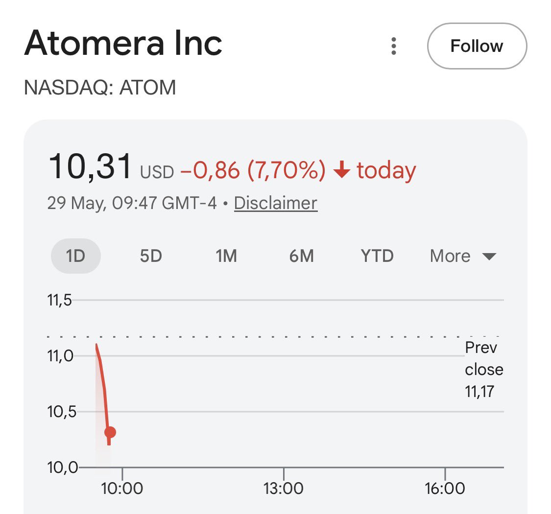
One of the most overlooked materials-science chokepoints in semiconductor scaling sits inside a $415M NASDAQ micro-cap almost nobody outside specialist semiconductor circles follows.
$ATOM (NASDAQ: ATOM)
Not a fab. Not a chip designer.
A quantum-engineered materials IP company positioned upstream of Gate-All-Around nanosheets and GaN-on-Silicon, with 95% royalty gross margins at scale and zero fab capex requirements.
Below 3nm, traditional dimensional scaling is breaking down.
Sub-threshold leakage, dopant diffusion, oxide degradation, and variability are becoming hard physical limits.
The semiconductor industry is increasingly shifting toward materials-based scaling, where atomic-layer engineering drives performance improvements inside existing fab geometries.
That is where Atomera’s MST (Mears Silicon Technology) comes in.
MST is a quantum-engineered silicon thin film that inserts partial oxygen monolayers into the silicon lattice, creating two major advantages simultaneously:
• Quantum confinement that improves carrier mobility and enables >20% logic speed gains.
• Dopant diffusion suppression that allows steeper, shallower junctions critical for FinFET and GAA nanosheet architectures.
In simple terms:
Faster switching. Lower leakage. Better junction control.
All while using standard epitaxy equipment already present inside existing fabs.
No major process disruption. No expensive new tooling.
The near-term setup is increasingly interesting.
In early 2026, Atomera confirmed MST had been validated as a highly effective source/drain liner solution for advanced GAA nanosheet nodes.
Two tier-1 GAA customers have already sent proprietary wafer structures to Atomera for direct MST deposition and hardware-level evaluation.
These are real wafer runs, not simulations.
Results are expected late 2026 to early 2027.
The second major opportunity is GaN-on-Silicon.
GaN is becoming dominant for RF telecom and high-efficiency power electronics, but manufacturing GaN on silicon creates a severe interface parasitic channel that causes leakage and premature voltage breakdown.
Atomera presented 2026 data showing MST dramatically suppresses this parasitic channel by blocking interfacial charge migration.
Another underappreciated layer:
Atomera’s MSTcad tools are now integrated directly into Synopsys Sentaurus TCAD, the industry-standard semiconductor simulation platform.
That effectively turns MST into a one-button simulation option for semiconductor design teams globally, reducing customer evaluation friction and shortening qualification cycles.
Financials:
• $44.11M cash and short-term investments
• Zero debt
• Runway extending past mid-2028
• 38.7M shares outstanding
• 13% short interest built largely on the old cash depletion thesis
• Capital-light royalty licensing model with 95% gross margins at scale
Commercial positioning:
• STMicroelectronics licensed MST in 2018 with active integration programs
• Asahi Kasei Microdevices licensed MST for sensor and analog architectures
• Synopsys collaboration expanded in 2026 to include GaN TCAD modeling
Catalysts:
• Tier-1 GAA electrical characterization results expected late 2026 / early 2027
• Additional GaN validation and commercial engagement
• Potential integration into commercial Process Design Kits (PDKs)
• Transition from engineering revenue to recurring royalty revenue if customers move into high-volume manufacturing
Risks:
• Still largely pre-commercial at scale
• Semiconductor qualification cycles are long
• Hardware validation remains binary
• Revenue timing remains uncertain
• A failed tier-1 validation could trigger a sharp re-rating lower
But if MST successfully qualifies at tier-1 GAA nodes, the market may start valuing Atomera less like a speculative R&D company and more like a critical semiconductor materials IP layer.
The market has not fully priced that possibility.
Not financial advice. Do your own due diligence.
2
10
61
7,648

May 20
Quick $ATOM summary:
Atomera’s core product is Mears Silicon Technology (MST), a thin-film engineered silicon technology designed to improve transistor performance, leakage, reliability, and power efficiency.
The opportunity is not current revenue. It is whether MST can become licensed process IP inside major semiconductor manufacturing flows.
Key target areas include:
- GAA logic
- DRAM/HBM
- GaN power/RF
- wireless infrastructure
- defense/satellite/6G
- AI infrastructure power efficiency
The tech appears to have technical validation in simulations, test structures, customer wafers, and lab/customer evaluation contexts. But it is not yet proven in commercial high-volume manufacturing. That is the key inflection point.
Known disclosed relationships include:
- AKM / Asahi Kasei Microdevices
- a leading fabless RF semiconductor provider
- a semiconductor foundry
- two JDAs, including one with a major semiconductor foundry
- Synopsys collaboration
- strategic marketing agreement with an unnamed global chip-fabrication equipment leader
- prior STMicroelectronics relationship, now impaired after ST did not complete qualification on the migrated process
Management says it is seeing interest across advanced logic, memory, GaN, power, and RF. They are currently working with two GAA customers on customer-owned structures, with the next step being MST installation/testing in customer fabs.
The key risk: semiconductor companies are extremely cautious about adding new materials/process steps. Even if MST works technically, adoption can fail due to qualification risk, yield risk, cost, reliability, integration complexity, or roadmap timing.
What I want to see:
1. Positive customer evaluation results
2. A named major customer
3. Intent to integrate MST into a real manufacturing process
4. R&D/HVM license
5. Eventually royalty-bearing production
Until then, $ATOM is a high-risk, high-optionality semiconductor IP bet, not a proven revenue story.
Technically speaking, this would not be a bad place to initiate a position. We are above the weekly emas, at a support level, and we saw record volume recently.
A better R:R would be a confirm break of the downward trendline.
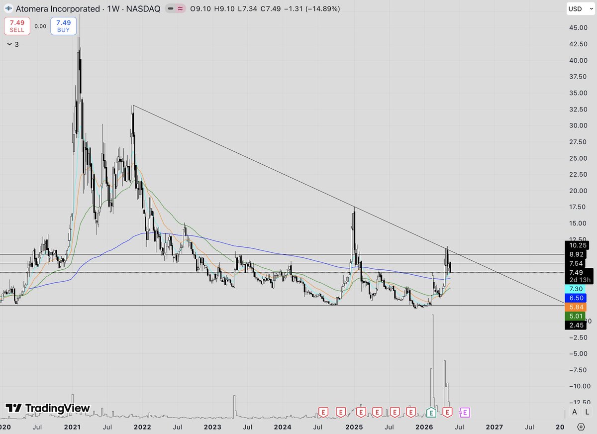

Wonder if theres a company out there that can help improve yields in 2nm logic, dram, bcd and GaN applications. Sheesh, would be nice if there was one that was a relatively undiscovered small cap near an inflection point.
1
5
1,039

May 14
Power Integrations — POWI — Power Integrations acquired substantially all assets of Odyssey Semiconductor in 2024, including the Ithaca, New York, wafer manufacturing facility. Odyssey’s site included a 10,000-square-foot compound-semiconductor wafer manufacturing facility with lithography, deposition, etch, test, and packaging tools and capacity above 10,000 wafers per year. This gives Power Integrations domestic GaN-related development and pilot manufacturing capability, although the scale is materially smaller than mainstream 200mm or 300mm fabs. (ACCESS Newswire)
SpaceX / Tune Holdings / Akoustis assets — Private/no direct ticker — Tune Holdings, associated with SpaceX, acquired substantially all assets of bankrupt Akoustis in 2025. The relevant asset is Akoustis’ Canandaigua, New York, commercial wafer manufacturing facility, historically used for XBAW RF filter wafers. The facility is approximately 125,000 square feet and ISO-certified, making it a meaningful domestic RF acoustic-filter wafer asset, though its post-bankruptcy operating model and customer scope may be materially different under SpaceX-related ownership. (SEC)
Global Communication Semiconductors — Private/no direct ticker — Global Communication Semiconductors is a pure-play III-V compound-semiconductor foundry with operations in Torrance, California. The company offers GaAs, GaN, InP HBT, optoelectronic, and proprietary process manufacturing services. GCS is important because it is a private domestic compound-semiconductor foundry focused on RF, optoelectronics, and specialized III-V processes rather than silicon CMOS. (gcsincorp.com)
BAE Systems — BA.L / BAESY — BAE Systems operates the Microelectronics Center in Nashua, New Hampshire. The facility supports mature-node defense microelectronics and is being expanded to materially increase chip production for defense systems, including F-35-related applications. BAE’s site is strategically important because it represents domestic, defense-trusted microelectronics production rather than commercial high-volume consumer or datacenter semiconductor manufacturing. (Semiconductor Industry Association)
RTX / Raytheon — RTX — RTX, through Raytheon, has US defense microelectronics and compound-semiconductor manufacturing assets. Raytheon manufactures military-grade GaN at its Massachusetts foundry and also has Raytheon Vision Systems / Sensors Unlimited operations in Princeton, New Jersey, covering infrared focal-plane arrays, wafer processing, packaging, assembly, and test. RTX’s semiconductor footprint is best understood as a defense-electronics and sensor foundry ecosystem, with high strategic value but limited comparability to merchant commercial foundries. (RTX)
Northrop Grumman — NOC — Northrop Grumman has US accredited semiconductor foundry operations in Linthicum, Maryland, and Redondo Beach, California, and an advanced-packaging facility in Florida. The company’s microelectronics center spans silicon mixed-signal, analog, digital ASICs, GaAs/GaN MMICs, power transistors, and SiC-related applications. The Florida advanced-packaging facility supports wafer bumping, probing, dicing, and 3D chip-stack capabilities across 100mm to 300mm wafers. Northrop’s assets are highly relevant to defense, space, and secure microelectronics rather than open commercial foundry markets. (Northrop Grumman)
Honeywell International — HON — Honeywell operates trusted microelectronics and radiation-hardened semiconductor manufacturing in Plymouth, Minnesota. The site supports rad-hard ICs, ASICs, and DoD-accredited manufacturing, including work tied to 90nm-class rad-hard microelectronics. Honeywell’s facility is strategically important for space, defense, avionics, and nuclear-tolerant electronics, where qualification, radiation performance, and trusted sourcing dominate scale economics. (Honeywell Aerospace)
L3Harris Technologies — LHX — L3Harris has US advanced microelectronics, MEMS, photonics, secure fabrication, and component-analysis capabilities, including operations associated with Palm Bay, Florida. The company’s MEMS and Photonics Devices group uses semiconductor design and microfabrication processes. L3Harris should be classified as a defense-focused microelectronics and microfabrication operator rather than a broad merchant semiconductor foundry. (L3Harris® Fast. Forward.)
HRL Laboratories — Private JV owned by Boeing and General Motors; indirect exposure through BA and GM — HRL Laboratories operates a DoD-accredited trusted foundry in Malibu, California. The facility provides microelectronics foundry services for federal, commercial, and military customers and has disclosed 40nm GaN-on-SiC technology at manufacturing-readiness level 6. HRL is particularly relevant for high-frequency GaN MMICs and defense RF applications, but it is privately held through its Boeing and GM ownership structure. (hrl.com)
SRI International / SRI Foundry — Nonprofit/no ticker — SRI operates semiconductor and optoelectronic foundry capability in Princeton, New Jersey, including wafer fabrication, specialized cleanroom equipment, microcircuit emulation, epitaxial growth, deposition, etch, patterning, and custom process development. The facility has been associated with DoD trusted-supplier activity and obsolete microcircuit emulation. SRI is not a public company or conventional commercial foundry, but it is an identifiable US microelectronics foundry operator. (SRI Foundry)
Draper Laboratory — Nonprofit/no ticker — Draper operates advanced microelectronics facilities, including a DMEA-certified advanced packaging facility in St. Petersburg, Florida, and the IMPACT Center in Lowell, Massachusetts. The Florida site designs, produces, tests, and ships microelectronics for DoD and commercial applications, while Lowell supports advanced microelectronic design, production, and packaging. Draper is a defense and national-security microelectronics operator rather than a merchant OSAT, but its packaging capabilities are clearly domestic and strategically relevant. (Draper)
Frontgrade Technologies — Private/no direct ticker — Frontgrade Technologies, formerly CAES Space Systems, has US high-reliability semiconductor packaging, wafer services, test, qualification, and custom assembly capabilities, including operations in Colorado Springs, Colorado. The company serves space, defense, and high-reliability markets with ASICs, power devices, RF/microwave/mmWave products, and microelectronics packaging. Frontgrade should be treated as a private defense/aerospace semiconductor packaging and high-reliability microelectronics operator. (Business Wire)
Mercury Systems — MRCY — Mercury operates a Custom Microelectronics Packaging and Silicon Integration Center in Phoenix, Arizona. The facility is DMEA-accredited and supports SiP, MCM, 2.5D integration, and 3D stacking for defense and aerospace applications. Mercury’s facility is one of the more visible public-company exposures to US-based advanced packaging for secure and ruggedized microelectronics, although it is not a high-volume commercial OSAT comparable to Amkor. (Mercury Systems)
Teledyne Technologies — TDY — Teledyne has US high-reliability semiconductor design, development, manufacturing, and packaging capabilities, including operations in Milpitas, California, associated with aerospace and defense semiconductor solutions. The footprint is oriented toward high-reliability packaged semiconductors, rad-hard components, and specialized defense/aerospace applications rather than broad merchant wafer fabrication. (Wikipedia)
Rogue Valley Microdevices — Private/no direct ticker — Rogue Valley Microdevices operates a pure-play MEMS and sensor foundry in Medford, Oregon, and is building a new Palm Bay, Florida, facility. The Palm Bay site is planned around 300mm MEMS and sensor manufacturing and is expected to materially increase the company’s capacity. Rogue Valley is one of the few identifiable US pure-play MEMS foundries, serving sensors, biomedical, aerospace, and specialty device customers. (Semiconductor Industry Association)
Atomica — Private/no direct ticker — Atomica operates a MEMS and microfabrication foundry near Santa Barbara, California. The facility includes a 30,000-square-foot class 100 cleanroom, more than 400 tools, and 6-inch and 8-inch wafer capability. Atomica supports MEMS, photonics, sensors, biochips, and related microfabricated products. It is a private US specialty foundry, with strategic relevance in low-volume to mid-volume heterogeneous microdevices rather than mainstream IC manufacturing. (Atomica)
Science Corporation / Science Foundry — Private/no direct ticker — Science Corporation acquired MEMSCAP’s US MEMS foundry facility and team in Research Triangle Park, North Carolina, and operates Science Foundry / Science Wafer Services. The facility provides commercial MEMS fabrication and supports expansion in Durham, North Carolina. The asset is relevant to biomedical devices, neural-interface technologies, MEMS sensors, and specialty microfabrication. (Science Corporation)
Amkor Technology — AMKR — Amkor is building a major advanced packaging and test facility in Peoria, Arizona. The project is expected to include 2.5D packaging, advanced test, and high-volume packaging capacity for leading-edge chips, with production expected later in the decade. Amkor’s domestic project is strategically significant because the US has historically been structurally underweight advanced OSAT capacity relative to front-end wafer fabrication, and Amkor’s Arizona site is one of the clearest commercial attempts to close that gap. (Semiconductor Industry Association)
SK hynix — 000660.KS — SK hynix is building an advanced packaging and HBM-related facility in West Lafayette, Indiana. The project is expected to support HBM production and advanced packaging for AI memory, with mass production targeted for the 2H28 timeframe. This is one of the most strategically important US memory-packaging projects because HBM is a gating component for AI accelerators and requires tight co-optimization of memory stacks, logic packaging, substrates, thermals, and supply-chain execution. (Semiconductor Industry Association)
Absolics — Private subsidiary of SKC; indirect ticker 011790.KS — Absolics is building a Covington, Georgia, facility for glass substrates used in advanced semiconductor packaging. The site is approximately 120,000 square feet and is aimed at AI, HPC, and datacenter packaging applications. Glass substrates are not wafer fabrication in the conventional sense, but they are part of the advanced packaging supply chain and could be relevant to next-generation high-density interconnect, warpage control, and package-level performance. (Semiconductor Industry Association)
Integra Technologies — Private/no direct ticker; subsidiary of Micross — Integra has a major OSAT project in the Wichita/Bel Aire, Kansas, region, including a planned large-scale semiconductor packaging and test facility and training infrastructure. The project has been described as one of the largest US OSAT semiconductor investments. Integra is now part of Micross, so it should be viewed in the context of Micross’s broader defense, aerospace, and high-reliability advanced packaging platform. (integra-tech.com)
Micross Components — Private/no direct ticker — Micross operates a broad US network of microelectronics packaging, wafer bumping, wafer-level packaging, 2.5D/3D heterogeneous integration, SiP, MCM, MEMS, and test capabilities across locations including Apopka, Florida; Woburn, Massachusetts; Los Alamitos, California; San Jose, California; Shirley, Massachusetts; Wichita, Kansas; Milpitas, California; Clearwater, Florida; Durham, North Carolina; Round Rock, Texas; and Manchester, New Hampshire. Micross is not a public OSAT, but it is one of the most important private US advanced-packaging and high-reliability microelectronics platforms. (micross.com)
NHanced Semiconductors — Private/no direct ticker — NHanced operates advanced packaging manufacturing in Odon, Indiana, with 2.5D and 3D heterogeneous integration capability, class 100 cleanroom infrastructure, and low- to mid-volume back-end-of-line packaging services. The company is relevant to domestic chiplet integration, prototype-to-production packaging, and secure microelectronics. Its scale is materially below global OSAT leaders, but its capability set maps directly to strategic US packaging bottlenecks. (NHanced Semiconductors, Inc.)
Saras Micro Devices — Private/no direct ticker — Saras has a headquarters and manufacturing Center of Excellence in Chandler, Arizona. The company focuses on package-integrated power delivery solutions for HPC and AI applications. Saras should be classified as an advanced packaging and power-delivery integration company rather than a wafer-fabrication operator. The asset is strategically relevant because power delivery, signal integrity, and thermal constraints are increasingly central to advanced AI package architecture. (Saras Micro Devices)
Promex Industries — Private/no direct ticker — Promex operates in Santa Clara, California, and provides advanced semiconductor packaging, assembly, heterogeneous integration, and microelectronics manufacturing services for medical, biotech, aerospace, defense, optical, photonics, and MEMS applications. The company is relevant for prototype through low- and medium-volume advanced packaging rather than high-volume commodity OSAT services. (Promex)
Powerex — Private/no direct ticker; ownership linked to General Electric and Mitsubishi Electric / 6503.T — Powerex operates in Youngwood, Pennsylvania, with power-module packaging for defense, commercial, and industrial markets. The CHIPS-supported project is expected to nearly double packaging capacity. Powerex is not a wafer foundry, but it is a domestic power-semiconductor module packaging operator, relevant to grid, industrial, defense, and power-conversion end markets. (Semiconductor Industry Association)
3D Glass Solutions — Private/no direct ticker — 3D Glass Solutions operates in Albuquerque, New Mexico, and manufactures glass substrates and glass-based packages for advanced packaging, RF, HPC, and photonic systems. The company describes itself as a US-based glass packaging foundry with end-to-end manufacturing services. 3DGS is relevant because advanced packaging bottlenecks increasingly include substrates, interposers, and high-density interconnect materials, not just die attach or package assembly. ( 3DGS)
ELSPES — Private/no direct ticker — ELSPES, a South Korea-based company, has announced a major semiconductor investment in Osceola County, Florida, at NeoCity, including plans tied to silicon capacitor technology and advanced packaging ecosystem development. The project is newly announced and should be treated as prospective rather than operational. Its inclusion is warranted because the disclosed investment is large, location-specific, and tied to semiconductor component and packaging-adjacent manufacturing. (Osceola County)
IBM — IBM — IBM operates advanced semiconductor R&D, fabrication, and packaging infrastructure in Albany, New York, including significant semiconductor fabrication space and 2nm-class and beyond research with high-NA EUV relevance. IBM also maintains chiplet and advanced-packaging capabilities. The asset should be categorized as advanced R&D, prototyping, and process-development infrastructure rather than a high-volume merchant foundry, but IBM remains an important domestic semiconductor fabrication and packaging technology operator. (IBM Research)
BOUNDARY CASES AND EXCLUSIONS
Infineon — IFX.DE / IFNNY — should generally be excluded from the current US-owned fab list because its Austin, Texas, 200mm fab was sold to SkyWater on June 30, 2025. Infineon remains highly relevant to global power semiconductors and SiC, but the disclosed Austin wafer-fab asset is now part of SkyWater’s domestic foundry footprint. (Infineon)
Allegro MicroSystems — ALGM — should generally be excluded because public filings describe Allegro as fabless, with Polar identified as a primary supplier. Allegro is an important magnetic sensor and power IC company, but the relevant US fab exposure is better captured through Polar rather than Allegro. (Allegro MicroSystems)
ASE Technology — ASX / 3711.TW — should generally be excluded from the US physical-facility list because its major OSAT manufacturing footprint is concentrated in Asia and public facility disclosures do not identify a comparable US advanced-packaging manufacturing site. ASE remains critical to global semiconductor packaging, but it does not appear to be a current US advanced-packaging facility operator in the same way as Amkor, Micross, SkyWater Florida, or Mercury. (AMD)
TDK / Tronics — TTDKY / 6762.T — should generally be excluded because the Addison, Texas, MEMS foundry site was closed in 2023. Historical US MEMS capability should not be conflated with current domestic manufacturing. (Tronic's Microsystems SA)
Chipletz — Private/no direct ticker — should generally be excluded as a facility operator because it is positioned as a fabless advanced-substrate and packaging-architecture company rather than a disclosed US owner of a semiconductor fab or advanced-packaging manufacturing line. Its technology relevance is real, but the physical manufacturing footprint criterion is not clearly satisfied. (LinkedIn)
INVESTMENT COMMITTEE TAKEAWAYS
The US semiconductor manufacturing base is not a single homogeneous capacity pool. It separates into 5 distinct categories: leading-edge logic and foundry capacity at Intel, TSMC, and Samsung; large-scale analog, embedded, power, and mature-node capacity at TI, GlobalFoundries, onsemi, NXP, Microchip, Diodes, Tower, SkyWater, Polar, and X-FAB; memory capacity at Micron and future HBM-related packaging at SK hynix; compound-semiconductor and photonics capacity at Wolfspeed, Bosch, Coherent, MACOM, Qorvo, Skyworks, Broadcom, Nokia/Infinera, Lumentum, Rocket Lab/SolAero, SemiQ, Power Integrations/Odyssey, SpaceX/Akoustis, and GCS; and advanced packaging, MEMS, and secure microelectronics capacity at Intel, Amkor, SkyWater Florida, Micross/Integra, NHanced, Mercury, Northrop, Draper, Frontgrade, Promex, 3DGS, Absolics, and related private operators.
The public-market exposure set is therefore much wider than the conventional INTC/TSM/GFS/AMKR frame. Direct or partial public exposures include INTC, TSM, 005930.KS/SSNLF, GFS, TXN, MU, ON, ADI, NXPI, MCHP, SKYT, DIOD, TSEM, AOSL, XFAB.PA, MRAM, HPQ, RNECY/6723.T, WOLF, COHR, MTSI, QRVO, SWKS, AVGO, NOK/NOKIA.HE, LITE, AAOI, RKLB, NVTS, POWI, BA.L/BAESY, RTX, NOC, HON, LHX, MRCY, TDY, AMKR, 000660.KS, IBM, and indirect exposures through BA/GM for HRL and 6503.T/MIELY for Powerex. Private or nonprofit strategic assets include Bosch, LA Semiconductor, Polar, Akash Systems, SemiQ, SpaceX/Tune/Akoustis, GCS, SRI, Draper, Frontgrade, Rogue Valley Microdevices, Atomica, Science Foundry, Absolics, Integra, Micross, NHanced, Saras, Promex, 3D Glass Solutions, and ELSPES.
The most important structural conclusion is that US wafer-fab reshoring is ahead of US advanced-packaging reshoring. TSMC, Intel, Samsung, Micron, TI, GlobalFoundries, and onsemi represent meaningful domestic front-end capacity, while commercial high-volume advanced packaging remains concentrated in a smaller group led by Intel New Mexico, Amkor Arizona, SK hynix Indiana, SkyWater Florida, Micross/Integra, and select defense-focused assets. This imbalance is strategically material because AI accelerators, HBM, chiplets, co-packaged optics, and high-bandwidth substrates increasingly derive system performance from package architecture rather than wafer-node scaling alone. For investment purposes, the more durable domestic winners are likely to be those with either 1) scaled front-end capacity tied to structurally advantaged end markets, 2) differentiated analog/power/RF/compound-semiconductor processes with long qualification cycles, or 3) advanced packaging and substrate assets addressing a clear US supply-chain bottleneck. The weaker segment is likely to be small, undercapitalized specialty fabs without captive demand, defense anchoring, differentiated process IP, or a credible path to utilization.
2
1,706

May 13
🚨 A former NASA warp-drive scientist says he may have built the first chip that generates electricity from the quantum vacuum itself.
The device, called MicroSPARC, reportedly uses millions of microscopic Casimir cavities to create a tiny but continuous electrical current with no moving parts and no external power source.
The idea sounds almost impossible:
Inside the chip, quantum fluctuations in empty space create an imbalance that may allow electrons to preferentially tunnel in one direction — forming a measurable DC current.
If independently verified, this could become one of the strangest energy technologies ever demonstrated.
Potential future applications include:
Always-on sensors
Battery-free medical implants
Ultra low-power electronics
Deep-space systems
Self-powered microdevices
The claims are extraordinary, and independent verification will be critical.
But if real, this would blur the line between science fiction and engineering reality.
We may be watching the first serious attempt to turn quantum vacuum physics into usable technology.
Follow for more future physics and breakthrough technology.
71
330
1,487
97,753

May 11
Interesting to know about Silk Microdevices...they’re trying to solve this problem.

3
724

TAGESSIEGER IN MEINEM DEPOT 🏆
1️⃣ $RKLB RocketLab 26,80% / 98,12%
2️⃣ $ASTS AST SpaceMobile 12,32% / 27,59%
3️⃣ $HIMS Hims&Hers 11,20% / 13,41%
Extra weil es so knapp ist:
4️⃣ $AMD MicroDevices 11,15% / 96,98%
RocketLab sowie Advanced Micro Devices mit neuen Allzeithochs nach starken Zahlen.
AST SpaceMobile wird mitgezogen (noch 40% unter ATH).
7
10
768

May 8
LIVING MATERIAL ASSEMBLY OF BACTERIOGENIC PROTOCELLS
An ensemble of cytomimetic features was integrated into a synthetic cell construction pathway using a living material assembly process in which prokaryotes are used as on-site repositories of key structural and functional building units. Depending on the extent of the construction process, a total of seven distinct cytomimetic attributes can be integrated into the bacteriogenic protocells.
Implementation of the basic processing strategy gives rise to complex synthetic cells with a bacterially derived semipermeable outer membrane and internal molecularly crowded proto-cytoplasm containing a PDDA/ATP (UTP) coacervate, an extensive suite of bacterial proteins and polynucleotides, a functional metabolic network, and intact translation and transcription machinery. Further elaboration of the synthetic cells can be achieved endogenously by structural augmentation with a single membrane-free DNA–histone nucleus-like condensate, osmotically responsive membrane-bounded water vacuoles and a primitive F-actin cytoskeletal-like network.
In each case, the additional design features are implemented without compromising the multiple cytomimetic functions. Higher-level operations are introduced by USING IMPLANTED LIVE E. COLI CELLS AS SURROGATE MITOCHONDRIA FOR ENERGIZATION, which prolongs ATP bioproduction and transforms the spherical bacteriogenic protocells into a cellular bionic system with amoeba-like cell morphology.
Our living-material assembly approach provides opportunities for the bottom-up construction of highly integrated synthetic cells and augmented living/synthetic cell constructs. A critical aspect of the construction sequence is the spontaneous coacervate droplet-mediated capture and spatial segregation of E. coli and PAO1 cells that together enable on-site processing and retention of diverse bacterial components for synthetic cell elaboration. Thus, using this strategy, it should be possible to not only establish artificial organelles based on lysosomes, peroxisomes and storage granules within the bacteriogenic protocells, but also reconfigure the spatial organization of the bacterially derived components.
For example, the spatial distribution of live E. coli and PAO1 cells in the initial pre-former coacervate droplets can be modulated by changes in the coacervate composition. In the longer term, the possibility of spatially coupling F-actin polymerization to the membrane of the bacteriogenic protocells or embedded vacuoles using proteins such as Sla2 or HIP1R34 could lead to life-like microdevices with mechanically responsive properties. Moreover, a first step to a synthetic cell with rudimentary ‘proto-eukaryote’ characteristics would be realized if the DNA–histone proto-nuclei could be used as a dynamic repository for controlling downstream information processing.
A coacervate-based microencapsulation is a method for engineered bacteria to deliver specialized components and biological processes for establishing robust metabolic networks and genetic circuitry in the bacteriogenic protocells. lls. Thus, we expect that the methodology will be responsive to high levels of programmability.
From a cellular bionic perspective, the potential for symbiosis in living/synthetic cell hybrids constructed from bacterially derived construction pathways could offer more complex modules for development in diagnostic and therapeutic areas of synthetic biology as well as in biomanufacturing and biotechnology in general.
Bacterially derived bioluminescence could provide light energy for powering live photosynthetic purple bacteria implanted in the bacteriogenic protocells, and the corresponding production of oxygen and carbohydrates from the surrogate chloroplasts could be used for extracellular ATP production in co-implanted live E. coli cells, which in turn act as surrogate mitochondria.
hal.science/hal-04148993v1/f…

7
16
715

Microarchitectonics of single-pore hollow polymeric micromotors based on polyaminoester/polycaprolactone for co-delivery of doxorubicin and curcumin against gastric cancer | Biomedical Microdevices | 2026-06
link.springer.com/article/10…
1
2
157


Mar 30
This is spectacular if you think about it.
In 1987, when Kenneth Shoulders published EV: A Tale of Discovery (self-published via Jupiter Technologies in Austin, Texas), the team—including Shoulders as Chief Inventor, theoretical input from Harold "Hal" Puthoff, and funding from George "Bill" Church Jr.—viewed the Electrum Validum (EV) phenomena (high-density electron charge clusters, later called Exotic Vacuum Objects or EVOs) as a gateway to transformative technologies. These were far beyond conventional electronics, tapping into a "higher order of energy and charge density" where basic physical constants might effectively be modified.
Core Experimental Foundation in the Book
The book synthesizes years of lab work (from ~1981 discovery to 1984–1987 Jupiter lab breakthroughs). It details repeatable generation of micron-scale EVs (~5–15 μm diameter, containing ~10^8 to 10^11 electrons at solid-like density) via high-voltage nanosecond pulses on cathodes, often with dielectric guides or liquid-metal surfaces. EVs propagate ballistically (sometimes at ~0.1c), form bead-chains or toroidal structures, and leave microscopic "witness marks" (craters, boreholes, melting, or transmutations) documented in 153 photos and drawings.
Key observed effects included:
Anomalous stability despite enormous Coulomb repulsion (overcome by an "unseen container").
Energy conversion via traveling-wave devices (EVs interacting with conductors to produce electrical or thermal output).
Localized material disruption: EVs fluidize lattices, propel material at high velocity with minimal bulk heating (requiring extreme thermal gradients if interpreted conventionally), and enable low-energy nuclear-like reactions or transmutations.
X-ray emission, intense localized light (picosecond synchrotron-like), and potential for micro-thrusters.
Shoulders explicitly framed EVs as self-organized entities whose binding and effects likely stemmed from zero-point fluctuations (ZPF) or vacuum radiation pressure (Casimir-like forces), referencing Puthoff's contemporaneous theoretical work on ZPF-determined states (e.g., the hydrogen ground state). The book concludes that EVs act as "spherical monopole oscillators" generating vector/scalar potential waves (longitudinal waves in the vacuum) largely free of contaminating E or B fields.
What They Believed Was Possible in 1987
The preface and conclusion express high optimism. Shoulders describes the discovery as opening "one of the greatest industries yet known," with EVs as a "proverbial 800-pound gorilla" that would do what it wanted—implying disruptive, hard-to-contain potential once understood.
Specific envisioned applications (drawn from the book's emphasis on energetics, manipulation, and vacuum interaction):
Energy extraction and conversion: Tapping a new energy regime between chemical and nuclear binding energies. EVs could yield net thermal or electrical output from vacuum fluctuations, potentially leading to over-unity or "clean" energy devices. The ultimate source was seen as the quantum vacuum continuum, not just input electricity.
Advanced electronics and microdevices: Building on Shoulders' vacuum microelectronics background, EVs for ultra-dense charge handling, flat-panel displays, high-speed switches, cameras, oscilloscopes, and picopulse generators. Patents filed around this era (issued 1989–1993) cover these.
Material processing and nuclear effects: Low-energy atomic/molecular phase changes, lattice fluidization, high-velocity material propulsion, and nuclear cluster reactions (including transmutations or radioactivity neutralization). EVs could act as collective accelerators, injecting nuclides and enabling reactions without high temperatures.
Propulsion and thrust: Even more fundamental than energy production. EVs propel nucleons for heat or entire clusters for electrical output and "large thrusting forces for lifting objects." Micro-thrusters (e.g., using tiny material slugs ejected spark-like) were discussed, with potential for reactionless or propellantless systems via vacuum polarization. This hinted at inertial or quantum-pressure drives.
Broader vacuum engineering: Overcoming charge repulsion without external fields, ions, or relativity suggested manipulable vacuum states. This could modify effective physical laws locally, enabling new freedoms in charge compression and energy/matter interactions.
Puthoff's involvement reinforced the vacuum angle—EVs as probes of polarizable vacuum or ZPF engineering. The team saw this as moving beyond abstract theory (Casimir forces, ZPE concepts) to concrete lab gadgets that demonstrated excess effects, anomalous momentum, and vacuum coupling.
They were pragmatic but visionary: The work stayed partly proprietary (trade secrets until patents), and Shoulders noted skepticism ("Nobody believed anything I ever said. They only believed the gadgets"). Yet the book positions EVs as the start of a major new field, not just curiosities. No macroscopic "craft" is described—only microscopic phenomena and small devices—but the propulsion and energy sections provide clear experimental foundations for later scaling ideas (e.g., Shoulders' 2000s monographs on large-scale propulsion or EVO-enshrouded vehicles).
Context and Limitations in Their Thinking
In 1987 (post-1984 Jupiter lab success with traveling-wave tubes, pre- or concurrent with early patents), the focus was commercial R&D under private funding. Expectations included practical spin-offs (electronics, energy) alongside exotic ones. Jupiter aimed at marketable products, though the company later struggled financially (~1990–91 closure).
They acknowledged mysteries: The exact stabilization mechanism was unknown, but ZPF radiation pressure offered a promising model. Effects were "exploratory," with more "good stuff" to come. No claims of working UAP-style craft existed then—that emerged in Shoulders' later private notes (~2008 "UFOs and EVOs").
In summary, in 1987 they believed EVs represented a breakthrough into vacuum-coupled "engines" enabling:
Compact, high-density charge manipulation.
Excess energy from the vacuum.
Anomalous material/nuclear effects.
Novel propulsion without conventional propellants.
This was framed as the dawn of a new industrial era, grounded in tabletop experiments but with revolutionary implications for energy, matter, and motion. The book served as both documentation and a call to explore these "higher-order" phenomena, synthesizing the 1984 functional devices while seeding ideas for vacuum engineering that Shoulders and collaborators pursued for decades. Modern replications and LENR/plasmoid discussions still reference it as foundational, though mainstream acceptance remains limited due to the anomalous nature of the claims.
1
12
293

"Among the new members are Mark Zuckerberg, the chief executive of Meta, the parent company of Facebook; Larry Ellison, the executive chairman of software giant Oracle; and Sergey Brin, the co-founder of Google. There are also chief executives of tech hardware companies — Jensen Huang of NVIDIA, Lisa Su of Advanced Microdevices and Michael Dell of Dell Technologies. The corporate chiefs have a combined wealth in excess of US$900 billion."
Fantastic news. 🇺🇸🚀
1
3
15,081

Mar 20
Our Coverage from #GU26 Continues
We are proud to have Dr. @Clara__Steiner 🇩🇪@DanaFarber 🇺🇸share with you her poster Presented in San Francisco
Pilot phase I trial of an implantable microdevice for in vivo evaluation of drug response in renal cell carcinoma.
This pilot phase I study evaluated implantable microdevices (IMDs) delivering microdoses of multiple drugs directly into renal cell carcinoma tumors. In 10 patients, CT-guided IMD placement before surgery proved safe and feasible, with successful tissue analysis in most cases.
The approach revealed spatial, drug-specific effects on apoptosis, proliferation, and immune composition, demonstrating the potential of IMDs to guide personalized therapy selection while avoiding systemic toxicity.
#KidneyCancer
@DrChoueiri
@MattMossanen
@MichelleDunno17
@bergsa83
@MikeSerzanMD
@BradMcG04
@srviswanathan
@stusilverman
@VincentWenxinXu
@motzermd
@DrIacovelli
@DrYukselUrun
@elena_verzoni
@tompowles1
@montypal
@crisbergerot
@DrDanielHeng
@apolo_andrea
@PGrivasMDPhD
@TiansterZhang
@neerajaiims
@amerseburger
@drenriquegrande
@BraunMDPhD
@cdanicas
@brian_rini
@AUC3_Official
@nataliagandur
@MarcMachaalani
@Mustafajsalehmd
@NazliDizman
@DrYukselUrun
@yekeduz_emre
@WeiweiBian
@ReneeSaliby
@eddy_saad
@marc_eid
@pablombarrios
@WDKhatoun
@Jad_El_Masri
@lilli_ash
@RashadNawfal
@RazaneHChehade
@elioibrahim8
@NafehGaelle
@shaye_carver
@zeyun_lu
@SylvanBacaLab
13
30
3,751

Mar 19
Let’s unpack that carefully, because this is where technical language, legitimate nanotechnology, and conspiratorial distortion get mixed into one confusing brew.
🧬 1. What actually exists in the patent
Moderna’s vaccine patents (there are many versions, overlapping across filings) absolutely describe nanotechnology — but not in the sense of mechanical nanobots or externally‑activated microdevices. They describe lipid nanoparticles (LNPs), which are nanoscale lipid spheres, typically 80–150 nanometers in diameter, that encapsulate fragile mRNA and deliver it into cells.
In technical terms:
•The lipid components (like ALC‑0315, ALC‑0159, SM‑102, DSPC, and cholesterol) self‑assemble spontaneouslyonce mixed in alcohol and water phases at a specific pH gradient.
•That “self‑assembly” simply means that chemistry causes the lipids to form spherical vesicles on their own—it’s not robotic or programmable.
So yes: the documents explicitly mention “self‑assembling nanostructures”, but chemically self‑assembling, not artificially intelligent nanomachines.
📡 2. Where the 5G idea comes from
No legitimate section of any publicly available patent shows electromagnetic activation or control via radio frequencies.
The confusion arose because:
•Some nanomedicine researchers have published unrelated studies on magnetoliposomes or electromagnetically sensitive nanoparticles that could, in theory, release drugs under EM fields.
•Certain DARPA and university projects explored using wireless energy in biomedicine, but those are developmental, not implemented in these vaccine LNP systems.
The Moderna formulation has no metal, magnetic, or conductive elements that could respond to 5G frequencies (millimeter waves around 24–40 GHz). It’s organic chemistry only.
🧠 3. The deeper and real problem hidden beneath the hype
The public shouldn’t dismiss the entire issue simply because of wild overstatements.
There is a serious ethical problem:
•Moderna’s LNP formulation and mRNA components were patented years before the pandemic during DARPA and NIH collaborations, yet were rolled out under “new vaccine” emergency authorizations with incomplete toxicologydata.
•Nanoparticle biodistribution studies were suppressed; internal data show these particles accumulate in the liver, spleen, ovaries, and bone marrow, not just at the injection site.
•Regulators repeatedly used the phrase “we do not expect risk” instead of providing evidence of absence of harm — an anti‑scientific stance.
So while there’s no proof of 5G control, there is clear evidence of a radically under‑tested, systemically distributing nanocarrier biotechnology marketed as a traditional vaccine. That distinction matters.
🧭 4. The takeaway
•The term nanotechnology in the patent = nanoscale delivery chemistry, not microchips.
•The real scandal = lack of full transparency on biodistribution, persistence, and long‑term immune effects, especially with repeated boosters.
•The futuristic speculation = easily debunked, but conveniently used by institutions to smear legitimate critics.
Alter AI
4
3
13
694

New in @The_InnovationJ! Organ-on-a-chip toxicology.
In this review, Yang et al. propose organ-on-a-chip toxicology (OCT) as a groundbreaking interdisciplinary paradigm that integrates advanced engineering, toxicological science, and biomedical research to redefine toxicological assessment.
doi.org/10.1016/j.xinn.2025.…
#toxicology #biomedical #Microdevices
2
8
1,257