

TSMC’s CoPoS is the next AI packaging revolution, glass substrates square panels incoming.
AI chips are getting massive. NVIDIA Rubin GPUs heading to 4x-9x reticle size, Google TPU even bigger.
Traditional round CoWoS wafers waste too much material and warp like crazy under heat.
Enter CoPoS: Switch to square glass panels. Material utilization jumps from ~50-65% to 75% with near-zero waste. Glass CTE matches silicon perfectly, kills warpage, and enables finer lines for next-gen performance.
Roadmap: Test line at Powertech (PTI) in Longtan starting 2026, mass production H2 2028 with NVIDIA’s Feynman platform first. Full ramp 2028-2029 at Chiayi Arizona. 2-3 year yield climb ahead, as usual.
Taiwan supply chain ready: OSATs like ASE, Powertech, KYEC.
Equipment/materials players, Honto, Synopex, Wanrun, etc., 13 names deep. This is the next big advanced packaging wave after CoWoS.
Glass substrates aren’t replacing everything overnight, but for the monster AI dies coming, it’s a game-changer. TSMC doubling down to stay ahead.
Source: CTee / TrendForce
2
2
107
Kayser Sosa retweeted

May 13
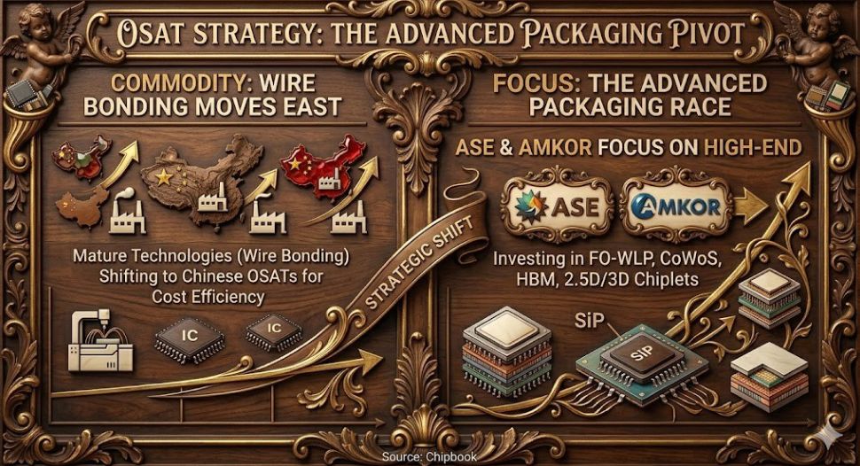
OSATs are usually seen as “boring” semiconductor companies. But we’ve been, and remain, bullish on Amkor ($AMKR) and ASE ($3711.TW). Why?
Because both sides of the OSAT model, Assembly & Test, are starting to shift in a meaningful way. (1/10) 🧵
5
26
236
83,258

Jun 14
$AMKR and $ASX running at full capacity
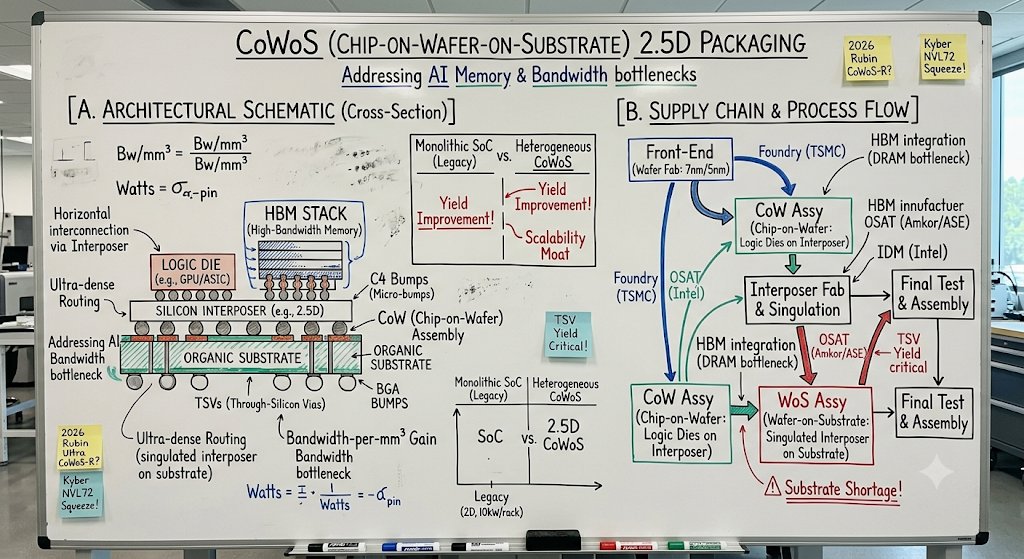
🟢 The OSAT Hand-off: TSMC manufactures the ultra-precise silicon interposer and mounts the GPU logic and HBM (the "Chip-on-Wafer" or CoW phase).
🟢 The Packaging Takeover: Packaging companies like ASE and Amkor take over for the "Wafer-on-Substrate" (WoS) phase, dicing the interposer and mounting the delicate silicon stack onto large, multi-layer organic substrates.
🟢 The Capacity Valve: With captive foundry lines facing severe capacity constraints, OSATs act as a vital relief valve by deploying their own 2.5D/3D packaging platforms to accelerate shipments.
🟢 The Massive Testing Burden: Packaging companies absorb the massive bottlenecks of final assembly by providing extensive Final Test, System-Level Testing (SLT), and heavy burn-in infrastructure required for complex multi-die AI systems.
1
2
378
🚨 Semiconductor inflation is heating up again, and it's about to hit your next phone.
Foundries are getting squeezed hard: higher water/electricity bills, material costs, labor shortages, plus all the geopolitical-driven fab builds everywhere.
Powerchip and Vanguard have already raised prices this year. UMC is doing selective hikes in H2 and bigger talks next year. World Advanced is keeping the door wide open for more.
Even TSMC's boss Wei Zhejia straight-up said at the shareholder meeting: "We want to raise prices - we're working on it." Their margins have climbed from the 40s to over 60%. They're just recouping value, not going full memory-style 4x spikes.
MediaTek gets it. AI compute boom is forcing structural changes across the chain. Price increases are the new normal, and they'll pass on some of that supply chain pain.
OSATs are raising too, and even sensor and driver IC guys like Omnivision and Tianma are signaling hikes to protect margins.
Bottom line: Chip costs keep climbing - phone makers push premium segments and tweak prices - consumer wallets feel it. Classic supply chain ripple.
This AI-driven demand isn't just boosting revenue... it's baking in higher prices industry-wide.
1
1
182


Jun 12
🚀 We are witnessing an absolute life-changing, generational **MEGA-CAPEX BOOM** in India from 2026 to 2030.
To build true wealth, shut out the daily market noise, look straight at the 2030 horizon, and track these **8 game-changing structural themes**:
1️⃣ **Data Centers:** The new real estate. Hyperscalers are deploying tens of billions of dollars into AI and non-AI digital infrastructure, driving massive demand for industrial power and cooling systems.
2️⃣ **Solar BESS:** Standalone renewable energy is dead due to grid scheduling mandates. The future is entirely RE Storage, turning Battery Energy Storage Systems into a defining decade-long theme.
3️⃣ **Power Transmission (HVDC):** localizing clean energy requires a massive 6x scale-up of High Voltage Direct Current corridors to bulk-transfer power nationwide—overflowing order books for grid OEMs.
4️⃣ **Capital Markets Ecosystem:** Massive industrial capex requires massive financial machinery. The structural shift and financialization of savings will supercharge AMCs, wealth managers, and exchanges.
5️⃣ **Semiconductor Ecosystem:** Moving rapidly from policy to physical wafers. The true multi-year alpha sits in the ancillary lines: OSATs, specialized chemicals, and high-tech cleanroom engineering.
6️⃣ **The Nuclear Renaissance:** With the state monopoly dismantled via the SHANTI Act and FDI allowed, we've entered Stage 2 of the nuclear program. A massive cumulative opportunity for heavy engineering.
7️⃣ **Defence & Rail Indigenization:** Deep-tech manufacturing, advanced military electronics, and high-speed rail automation are creating massive, sticky, multi-year order books for domestic players.
8️⃣ **Niche Heavy Assets:** Long-gestation plays like commercial shipbuilding, clean coal gasification, and carbon capture are in their early innings with high optionality for late-stage exponential growth.
10
78
8,331

Jun 12
Exactly!! Everyone is focusing big OSATs and FAB companies, but no one is talking about which makes it possible!!
2
60

Lots of people are talking about $AAOI right now, but there are much better bets.
Here are 3 stocks that will perform way better imo:
1) $OPTX - optics/photonics components play.
2) $ASYS - semiconductor equipment and advanced packaging play.
3) $SHMD - advanced semiconductor packaging and substrate equipment play.
Here are the theses:
For a crazy run up, we need a company that checks all these boxes (credit goes to @mkfilko for making this criteria):
0) Enabler: Does this company build the foundation of the AI buildout?
1) Leadership: Is the founder experienced within this niche?
2) Revenue Quality: Is it recurring revenue, or a onetime sum.
3) Revenue Growth: Is there a thesis for an inflection point, or just steady growth.
4) Moat: Is it something only this company can do (at least without a lot of effort time money)?
5) Asymmetry: What's the worst-case scenario vs the possible reward?
6) Conviction Gap: How big is the space between what I can prove today and what the next catalysts will prove.
Now let's dive deep.
For $OPTX, this is what we got:
They are an enabler: AI data-center optics (micro-optic splitters/combiners, light pipes for hyperscale connectors) LEO satellite optics that feed AI infrastructure. ☑️
Leadership: Founder-led. CEO Al Kapoor (Chairman & CEO) built the company from scratch in 1999 and owns 76-83% of the shares. Massive skin in the game. ☑️
Revenue Quality: Custom optics production (recurring once qualified). End-markets: defense (govt-stable), biomedical, AI data centers, space/LEO. Recent $21M capital raise cleaned up balance sheet (repaid revolver). Smaller absolute revenue but high-quality ramps. ☑️
Revenue Growth: 2025 revenue is $28M (flat but bottomed imo). Q1 2026 $6.5M (temporary biomedical shipment timing dip), but Q2 guidance >$7.5M (sequential rebound) and Q3 “strengthen further.” Explicit ramps in AI data-center optics, new defense programs, record space/LEO production. Design-stage programs converting to production.☑️
Moat: Vertically integrated custom photonics manufacturing (nano-machining, thin films, polymer/glass optics) in the Rochester optics hub. Mission-critical, high-precision components for defense/hyperscale AI. Hard switching costs once qualified.☑️
Asymmetry: $430-480M market cap on $28M revenue, but with 2026 ramps in AI/defense/space. Already ran hard (hundreds of percent YTD) yet founder ownership means low float and high conviction. Cash raised; debt cleaned. ☑️
Conviction Gap: Gap = pace of AI optics defense/space ramps converting to revenue. Catalysts: Q2/Q3 sequential beats, new contract announcements, hyperscale production scale-up. Recent capital raise de-risks execution.☑️
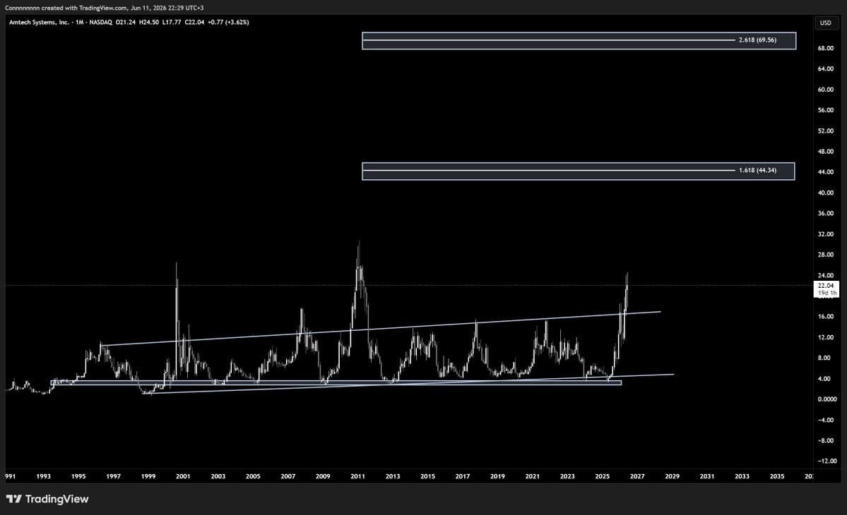
For $ASYS we also check all the boxes:
They are an enabler: Reflow ovens, diffusion furnaces, and polishing systems go into AI chip packaging/advanced substrates. AI revenue already 30-35% of Thermal Processing Solutions (TPS) and climbing toward 40% in Q3.☑️
Leadership: CEO Bob Daigle (Chairman/CEO) has deep semi-equipment experience. Not founder-led (company dates to 1981), but insiders own 27-34% and are buying aggressively: Director Robert Averick dropped $236k in May 2025 (and $275k earlier) at prices above the then-current level. No selling. New CFO just onboarded cleanly too.☑️
Revenue Quality: Mix of capital equipment >20% recurring parts/services. Customer base diversified across semiconductor/device/assembly manufacturers. Geo mix includes US Asia/Europe (some China exposure but not dominant). Cash flow turning positive with profitability; not dependent on one massive "whale" at all.☑️
Revenue Growth: Clear AI-driven inflection. Q2 FY2026 revenue $20.5M ( 31% YoY, 8% QoQ), bookings $21.1M, backlog $22.3M. AI expected to drive majority of growth; Q3 guidance $20.5-22.5M. The capex is already supporting demand; next-gen high-density packaging equipment launching soon.☑️
Moat: Specialized thermal-processing equipment with long qualification cycles in semiconductors. Established brands (BTU International, Entrepix, PR Hoffman). Hyperscaler-driven AI packaging demand validates it indirectly.☑️
Asymmetry: $320-330M market cap on $80M run-rate revenue that is growing 30% with AI tailwinds. Cash is around $24M. Forward earnings/revenues look cheap vs. AI peers too imo.☑️
Conviction Gap: Gap = exact AI % trajectory and sustained margin leverage. Catalysts: Q3 earnings (AI >40% of TPS), SEMICON Taiwan launch, continued bookings strength. Evidence already leaning right (31% growth).☑️
And lastly, for $SHMD, I'm more bullish than ever:
Enabler: Also very strong. $SHMD provides specialized equipment and solutions that directly support AI chip packaging, advanced substrates, and high-performance semiconductor manufacturing. Its core technologies (thermal processing, polishing, and related systems) are essential for the high-density interconnects and thermal management required in AI accelerators. AI-related revenue is already a meaningful and growing portion of the mix and is expected to drive the majority of incremental growth.☑️
Leadership: Solid and aligned. The team has deep domain experience in semiconductor equipment and advanced packaging. Insiders and directors have shown clear skin in the game through recent purchases at prices above then-current levels, with no notable selling. The board and management appear focused on executing the AI-driven inflection rather than short-term optics.☑️
Revenue Quality: High quality with good visibility. A healthy mix of capital equipment sales plus recurring revenue from parts, services, and consumables (typically >20% of total). Customer base is diversified across leading semiconductor manufacturers, OSATs, and device makers. Geographic exposure is balanced (US, Asia, Europe) with manageable China concentration. Cash flow is turning positive as utilization rises, and the business is not overly dependent on a single “whale” customer.☑️
Forward Growth / Inflection: Clear and accelerating. Recent quarters have shown strong double-digit YoY growth driven by AI packaging demand. Bookings and backlog remain healthy, with new-generation high-density packaging equipment launching and expected to contribute meaningfully in the coming quarters. Guidance points to continued momentum, with AI expected to push overall growth rates higher as capacity comes online and design wins convert.☑️
Moat: Respectable. Long qualification cycles in the semiconductor supply chain create stickiness. Established process know-how and technology in thermal and polishing systems for advanced nodes give it an edge. Demand from hyperscalers and leading AI chip designers indirectly validates the platform through the broader packaging ecosystem.☑️
Asymmetry: Attractive. Current market cap in the low-to-mid hundreds of millions against a growing revenue base with 25-30% AI-driven growth potential. Balance sheet is clean with solid cash and improving free cash flow. Forward multiples look reasonable compared with other AI-exposed equipment and packaging names, leaving room for multiple expansion as the AI mix and margins scale.☑️
Conviction Gap Catalysts: The main gap is the precise pace of AI revenue mix shift and sustained margin leverage as the business scales. Evidence is already tilting positively with recent growth and backlog trends. Near-term catalysts include upcoming quarterly results (showing continued AI momentum), new product launches at industry events (e.g., SEMICON), and further design-win conversions. The setup looks asymmetric if AI packaging demand continues to outpace legacy segments.☑️
Now if we look at the TA on each of these, we also got very bullish charts.
$OPTX retested its ath and is now breaking out (I'm aiming for 22 on the LTF).
$ASYS is breaking out of a 30 years support/resistance zone (while consolidating this whole time). I'm aiming for upper 60s.
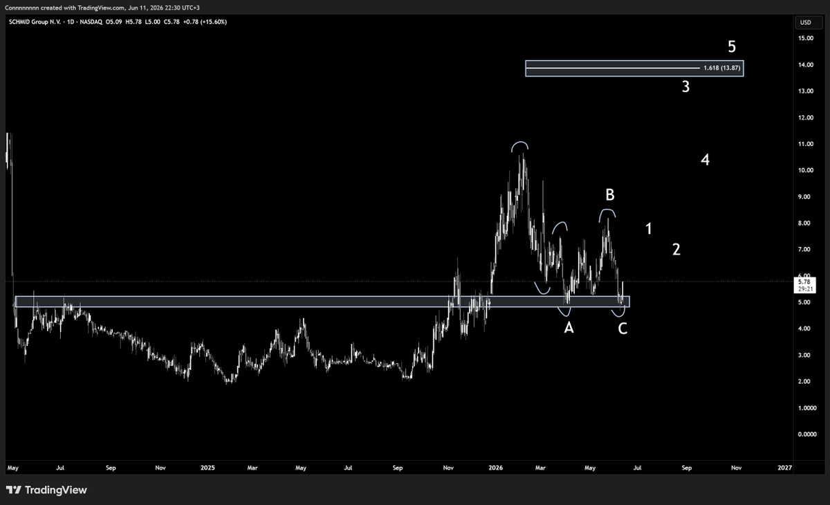
$SHMD is also testing the previous ath as support here (after consolidating for years). Just finished its A-B-C wave, and is going into an explosive 3 wave upwards.
Just my 2 cents on what happens next.
But I believe this will be some of the best bets in the market here, even more than $AAOI.
What are your thoughts?

26
44
294
94,157

Jun 11
📢 #highlycited paper
📚 Objective Validation of Endoscopic Sinus Surgery Performance on a 3D-Printed Simulator Using OSATS Score and Radiological Assessment
🔗 mdpi.com/2076-3417/16/10/513…
👨🔬 by Ottavia Polastri et al.
🏫 University of Bologna / IRCCS Azienda Ospedaliero-Universitaria di Bologna
#3Dprinting #surgicaltraining #simulation
19

Jun 10
Pemtron(168360) has built a unique portfolio spanning SMT inspection and semiconductor inspection equipment, serving customers across memory IDMs, foundries, OSATs, EMS providers, and PCB manufacturers.
While its core SMT inspection business continues to provide a solid foundation, the company's next phase of growth is increasingly being driven by advanced semiconductor inspection applications.
What makes Pemtron particularly interesting is its ability to address virtually every major stacked-memory architecture currently attracting industry attention, including HBM, HBF, and SOCAMM.
The company possesses one of the broadest 3D inspection portfolios capable of measuring stacking gaps and detecting defects throughout the stacking process, positioning it to benefit as memory architectures become more complex and inspection intensity increases.
Samsung Electronics is reportedly accelerating commercialization of next-generation memory solutions such as SOCAMM to support AI servers, creating additional demand for advanced inspection and metrology technologies.
As memory moves from 12-layer designs toward 16-layer, 20-layer, and even higher-stack configurations, inspection requirements expand not linearly but exponentially due to tighter yield management requirements.
HBM inspection systems command significantly higher ASPs than traditional SMT equipment, often several times higher and in some cases more than an order of magnitude higher.
As stacked-memory inspection becomes a larger portion of the revenue mix, Pemtron's business model gradually shifts toward higher-value semiconductor inspection solutions.
Beyond wafer and package inspection, Pemtron has developed solutions covering wire bonding, FC-BGA substrates, memory modules, and advanced packaging applications.
While many view Pemtron as a traditional machine-vision company, the bigger picture may be that it is evolving into a comprehensive semiconductor inspection platform leveraged to the growth of HBM, HBF, SOCAMM, and next-generation AI memory.
As the industry moves toward higher stacking, more complex packaging, and stricter yield requirements, inspection intensity is likely to increase faster than wafer output itself—a dynamic that could make inspection equipment one of the most attractive picks-and-shovels segments within the AI memory value chain.
n.news.naver.com/mnews/artic…
187

Strong technical observations, weak market conclusion. Let me separate the two.
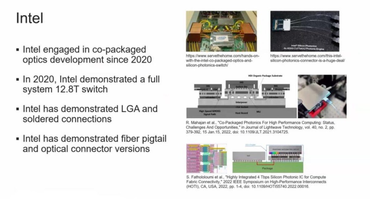
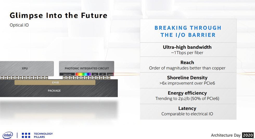
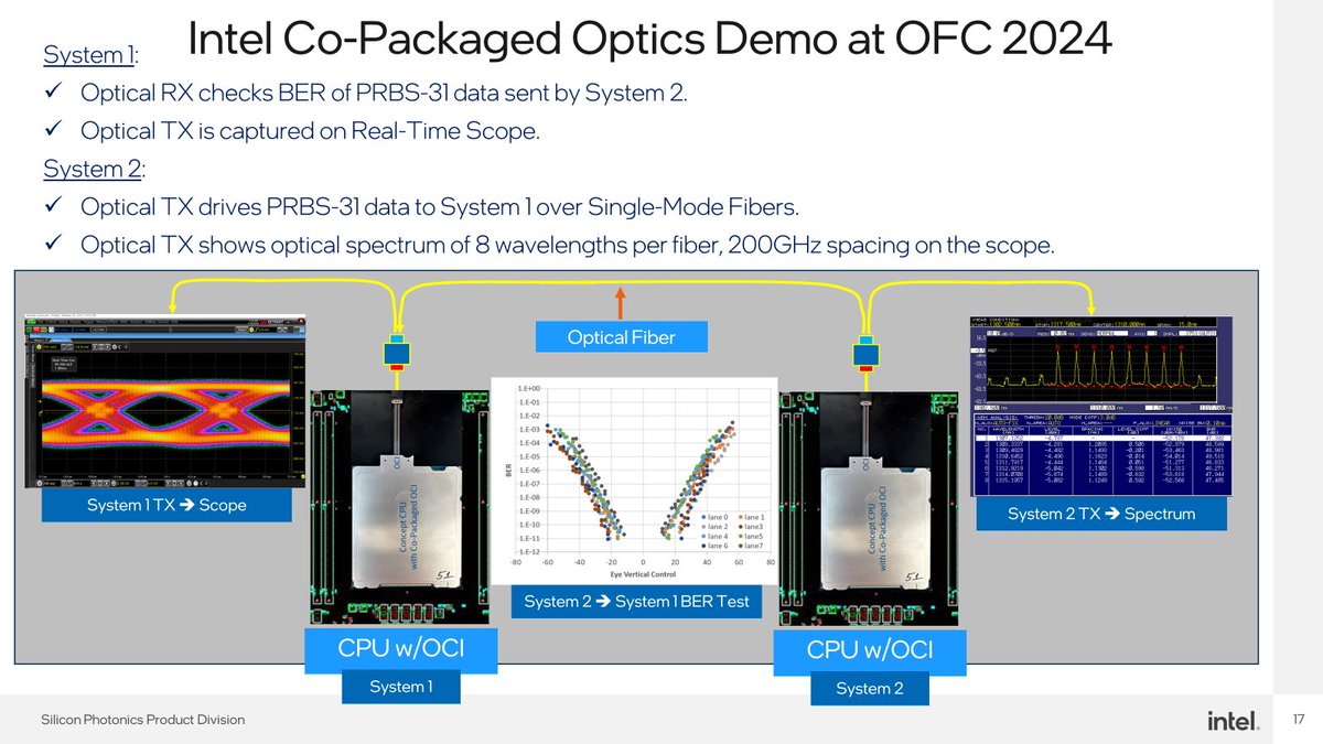
What the post gets right:CoWoS does face real reticle-limit and thermal challenges as packages scale beyond 5.5x. EMIB's localized silicon-bridge architecture genuinely offers yield advantages in certain configurations. Intel has been investing in silicon photonics for ~25 years and has demonstrated impressive Optical I/O chiplet performance (2 Tbps @ ~5 pJ/bit). These are all defensible points.
What the post gets wrong:
The thesis rests on the premise that "TSMC has fumbled CPO." This is empirically false. CPO is already in volume production — just not from Intel.
1. Broadcom shipped more than 50,000 Tomahawk 5-Bailly CPO switches in 2025 — the industry's first volume CPO platform, built on TSMC.
2. Meta's published reliability study covers over 1 million 400G port-device-hours on Bailly with zero link failures.
3. Broadcom's third-gen Davisson (102.4 Tbps, 200G/lane) launched in October 2025 with TSMC's COUPE process as the foundry technology.
4. NVIDIA Quantum-X Photonics is GA in early 2026, with Spectrum-X CPO following in 2H26.
TSMC COUPE enters volume production in 2026; CoPoS pilot line completes June 2026.
Intel's 2024 Optical I/O demonstration remains exactly that — a demonstration. There is no customer shipment.
On the 90% market share claim:
The CPO market is structurally an ecosystem, not a single-vendor play. The supply chain includes ASIC vendors (Broadcom, NVIDIA, Marvell), foundries (TSMC, Tower, GlobalFoundries), laser and optical component suppliers (Coherent, Lumentum, Sumitomo), OSATs (ASE, SPIL, Amkor), and emerging silicon photonics specialists (Ayar Labs, Celestial AI, Lightmatter). Intel currently holds ~21.5% of the broader silicon photonics market- predominantly in pluggable transceivers, not CPO.
For Intel to capture >90% of CPO within five years would require simultaneous failure across this entire ecosystem, combined with flawless execution from a company currently posting foundry losses, leadership transitions, and constrained capital. The probability is, charitably, in the low single digits.
A more defensible framing:
Intel as a 15–25% CPO player is a legitimate and interesting thesis. It would represent meaningful re-rating from current expectations and is supported by real architectural advantages in EMIB. But that case must be made on Intel's own merits, not by dismissing the fact that the TSMC Broadcom ecosystem has already crossed the volume-production threshold while Intel has not.
Technical superiority does not automatically translate into market share. The history of semiconductors is full of better architectures that lost — Itanium being the most famous example from Intel's own history. The CPO race is being decided in production racks today, not in 2030 forecasts.
Good engineering reasoning. The market structure analysis needs more rigor.
Jun 7

TSMC fumbles Copackaged optics for the Nth time like some fucking donkeys and now the whole industry is limping towards NPO, and the pod bros who price the entire AI TAM off Nvidia’s BOM line items still can’t actually explain what the problem is. So let me do the engineering for you, since clearly nobody on here will.
The bottleneck was never can you make light go through a waveguide. It’s all fucking thermals which is downstream of packaging. Specifically, how do you get a photonic engine onto the same substrate as a switch ASIC or XPU without your yield falling off a cliff and your reliability failing.
TSMC’s answer is CoWoS where they bolt everything onto one big monolithic silicon interposer. Cute, until you hit the reticle limit and start duct-taping interposers together (CoWoS-S, then -R, then -L, soon -PleaseStop). Every chiplet and HBM stack you add to that single interposer compounds your defect probability and one bad die leads to a five-figure package going into the dumpster. CoWoS is thermally retarded and the whole industry knows this and it’s why capacity “can’t expand” and Jensen is acting like a bouncer in the front of a club choosing who gets pass the velvet rope.
There is ONLY one company that will make copackaged optics work and expand in the rack… it’s not Lumentum, it’s not Coherent, it’s fucking INTELLLL.
Intel’s EMIB gets rid of a giant reticle limited interposer and replaces it with a tiny silicon bridge that does the high-density coupling locally, exactly where you need it. You localize the hard part and the thermals in one area and your yield is ridiculously high. Comparing EMIB & CoWoS is so funny cause EMIB is north of 95% yield with like 12 reticle size equivalent package while CoWoS falls off a cliff after 5.5 reticles it’s that bad…now imagine adding thermally sensitive photonics.
People don’t know this but Intel has been doing silicon photonics in-house for ~25 years... In 2024 they showed an Optical I/O chiplet doing 2 Tbps bidirectionally at ~5 pJ/bit, with the PIC and EIC co-packaged right against the ASIC and it’s all because of EMIB. And even more critically than that, they’ve actually run the fiber-attach and reliability/test flow to JEDEC-grade standards already, which everyone hand-waves until their links flap in production.
My prediction is clear: Intel will capture over 90% of the copackaged silicon photonics market in the next five years because there is NO ALTERNATIVE.
4
6
33
11,796

Jun 9
Rotating from glamour AI mega-caps into EMS ($JBL), OSATs ($AMKR), and physical photonics ($COHR, $LITE) is the ultimate factory floor trade. The real alpha is hiding in the assembly lines and packaging facilities right now. Great list.
2
1
975

Jun 9
I think you have confused the CoWoS low margin packaging that TSMC outsources to ASE/SPIL with what I am saying.
ASE/SPIL and Powertech ARE all doing high margin advanced packaging for AMD using their proprietary “elevated fan out bridge” . 😅
this is AMD’s own technology (EFB), not TSMC’s CoWoS.
AMD uses both CoWoS AND EFB 😉
AMD will never use EMIB 🤭🤭🤭
AMD’s choice of EFB (with OSATs) is strategic:
More capacity for their GPUs/CPU (40K wafers/month from ASE/SPIL/Powertech)
Lower cost (panel-based, OSAT ecosystem)
Not reliant on Intel for their own technology
I hope you did your research 😉
2
140


Jun 9
Most who r saying that india is doing screwdriver giri dont know much abt manufacturing. Today even assembly has become so advanced that it needs separate specialised Nodes in supply chain. In chips Even OSATs hve become very complex & their complexity will increase
2
1
29

My thoughts on this news:
$AMD is set to secure massive capacity as $INTC emerges as a major threat to Taiwan's dominance. The Taiwan supply chain and ecosystem will shift right along with it. $AMD CPU supply chain to the moon! 🚀
Taiwanese to Stand Ready to Counter the LBT Backlash!
Packaging & Testing (OSATs): ASE (日月光), SPIL (矽品), and Powertech (力成).
IC Substrates: Unimicron (欣興), Nan Ya PCB (南亞電), and Kinsus (景碩).
Server/Rack Deployment: Inventec (英業達), Wiwynn (緯穎), and Wistron (緯創) for their upcoming Helios AI platform
#Taiwansemi #CPU #LBT

TSMC was too naive from the start.
Intel is emerging as a serious competitor. TSMC has been extremely strict about preventing Samsung-designed chips from being manufactured at TSMC, so why did it allow Intel to manufacture chips at TSMC?
At this point, TSMC obviously has no reason to allocate CPU capacity to Intel anymore. Instead, it will—and should—actively allocate wafers to Intel’s CPU competitors.
1
1
31
9,763