
Joined February 2026
- Tweets 466
- Following 124
- Followers 244
- Likes 395
11 Photos and videos


Dracaena retweeted

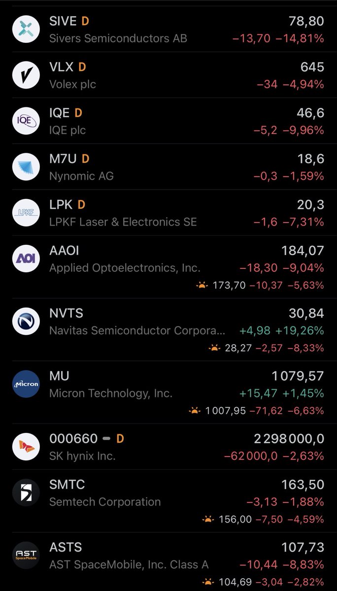
$CIEN beat EPS by 12%, grew revenue 40% year over year, and raised full year guidance to $6.3B. The stock is 30% off its high.
The selloff had nothing to do with the business. Full year guidance came in at $6.3B. The street was modeling $6.29B. When a beat-and-raise lands exactly on consensus after a 200% run, the exit happens automatically. The $2.875B convertible offering that followed added mechanical selling pressure from hedge counterparties through its June 11 close.
Gary Smith on the call: "Visibility remains strong, well beyond our historical norms."
Hyperscalers are stitching together GPU clusters across cities, countries, and continents into a single logical training environment. The coherent optical fiber running between those sites at 800G and 1.6T is the backbone of every continentally connected AI data center being built today. That is what $CIEN builds. Number one globally in data center interconnect. Addressable market doubles to $50B by 2029. This is scale-across.
$7.7B backlog. Stock is 30% off its high with both selloff catalysts cleared.


The AI infrastructure buildout has three distinct networking layers. Each one is at a different point in its adoption curve and each one has different winners.
1. Scale-up connects GPUs inside a single server and eventually across racks. The transition from copper is happening in stages.
> Copper still dominates at short distances.
> Active electrical cable extends that reach but loses signal integrity as clusters grow.
> LPO removes the DSP entirely, cutting power consumption to near CPO levels while keeping the pluggable form factor operators already know.
> NPO moves optics closer to the chip without full co-packaging. Both are ramping faster than CPO in the near term because they require less ecosystem disruption.
> CPO is the endgame. It integrates optics directly onto the switch ASIC substrate, cutting signal loss from 20dB to 1-2dB and power consumption by 3x or more.
$AVGO's Davisson and $NVDA's Spectrum-X are the CPO platforms. $MRVL acquired Celestial AI to position optics directly on top of XPUs rather than at the die edge, with Amazon as the lead design win. $COHR and $LITE supply the CW and EML lasers every platform requires. $LITE holds more than 50% share in high-speed EML lasers with multi-billion dollar supply agreements locked with Nvidia through end of decade. $CRDO and $MTSI supply the LRO and LPO chipsets capturing near term volume before CPO fully ramps.
2. Scale-out connects servers inside a single data center. The 800G transceiver cycle is at peak volume with 1.6T at the beginning of its inflection.
> $MRVL's 51.2T switches and DSPs sit at the center.
> $AAOI is expanding capacity 10x and demand still outpaces supply through mid-2027.
> $COHR supplies modules across the stack.
3. Scale-across connects data centers to each other over distance so one AI model trains across geographically distributed GPU clusters as a single logical environment. The link between sites requires lossless coherent optical transport at 800G and 1.6T.
> $CIEN holds the number one global position in data center interconnect. Their Q2 executive summary states it directly: "DCI, including scale-across, is gaining momentum as customers connect AI data centers to monetize their investments."
> $COHR and $LITE supply the optical circuit switches enabling spine replacement and redundancy across those links.

17
10
118
26,867
Dracaena retweeted

Here's the alpha list.
Bookmark and use it for the next 10 years.
If you find it useful, please throw in a like / share.
LAYER 1: APPLICATION
AI Assistants & Chatbots:
Microsoft, Google, Meta
Enterprise AI SaaS:
Microsoft, Salesforce, ServiceNow, Adobe
AI-Native Vertical Apps:
Recursion Pharmaceuticals
LAYER 2: AI MODEL
Foundation Models:
Google, Meta
Fine-Tuned / Specialized Models:
LAYER 3: SOFTWARE INFRASTRUCTURE
ML Frameworks:
Google
GPU Programming Layer:
NVIDIA, AMD, Intel
Distributed Training Systems:
Microsoft
Container Orchestration:
IBM, Broadcom
Inference Optimization Stack:
NVIDIA
LAYER 4: CLOUD INFRASTRUCTURE
Hyperscaler Clouds:
Amazon, Microsoft, Google, Oracle
NeoClouds:
CoreWeave, Nebius
Edge / Inference Clouds:
Cloudflare, Fastly, Akamai
Data Center Colocation:
Equinix, Digital Realty, NTT
LAYER 5: COMPUTE HARDWARE
Training GPUs:
NVIDIA, AMD
Inference GPUs:
NVIDIA, AMD, Intel
Custom AI ASICs:
Google, Amazon, Microsoft, Meta
Dedicated Inference Accelerators:
Cerebras
Server CPUs:
AMD, Intel, NVIDIA, SoftBank
Networking ASICs / Switches:
Broadcom, NVIDIA, Marvell, Cisco
LAYER 6: MEMORY
HBM:
SK hynix, Samsung, Micron
DRAM:
Samsung, SK hynix, Micron
NAND Flash:
Samsung, Kioxia, Western Digital, Micron
LPDDR:
Samsung, SK hynix, Micron
LAYER 7: INTERCONNECT
Co-Packaged Optics:
Broadcom, NVIDIA, Marvell, Cisco
NVLink / Fabrics:
NVIDIA, AMD, Astera Labs, Broadcom
Optical Transceivers:
Coherent, Lumentum, Innolight, Eoptolink
Linear Pluggable Optics:
Credo, Marvell, Broadcom, Lumentum
Ethernet / InfiniBand:
NVIDIA, Broadcom, Cisco, Arista
Coherent Optical Transport:
Ciena, Nokia, Cisco
Long-Haul DWDM:
Ciena, Nokia, Cisco, Fujitsu
Submarine & Metro Fiber:
NEC, Prysmian
External Light Sources:
Coherent, Lumentum, Intel
Optical Connectors:
Corning, Amphenol
Optical Engines:
Broadcom, Marvell, Coherent
Fiber Cables:
Corning, Prysmian, Furukawa Electric
LAYER 8: ADVANCED PACKAGING
Wafer-Level Packaging:
TSMC, ASE Technology, Amkor, Samsung
HBM Integration:
SK hynix, Samsung, Micron, TSMC
FC-BGA Substrates:
Ibiden, Unimicron, Shinko Electric, AT&S
Glass Core Substrates:
Intel, Samsung Electro-Mechanics, Corning
Thermal Interface Materials:
Henkel, Shin-Etsu Chemical, Honeywell, Parker Hannifin
LAYER 9: SEMICONDUCTOR FOUNDRY
Leading Edge Foundry:
TSMC, Samsung Foundry, Intel Foundry
Mature Node Foundry:
GlobalFoundries, UMC, Tower Semiconductor, Vanguard International
Silicon Photonics Foundry:
GlobalFoundries, TSMC, Intel
Compound Semiconductor Foundry:
Wolfspeed, Qorvo, MACOM, WIN Semiconductors
OSAT:
ASE Technology, Amkor, JCET, Powertech Technology
LAYER 10: SEMICONDUCTOR EQUIPMENT
Lithography:
ASML, Nikon, Canon
Deposition:
Applied Materials, Lam Research, Tokyo Electron, ASM International
Etch:
Lam Research, Tokyo Electron, Applied Materials
Burn-In & Reliability Testing:
Advantest, Teradyne, Cohu, Aehr Test Systems
Metrology & Inspection:
KLA, ASML, Onto Innovation, Hitachi High-Tech
Compound Semiconductor Growth:
Aixtron, Veeco, Taiyo Nippon Sanso
LAYER 11: SEMICONDUCTOR MATERIALS
Silicon Wafers:
Shin-Etsu Chemical, SUMCO, GlobalWafers, Siltronic
SOI Wafers:
Soitec, Shin-Etsu Chemical, GlobalWafers
InP Substrates:
AXT, Sumitomo Electric
GaAs Substrates:
AXT, Sumitomo Electric
SiC Wafers:
Wolfspeed, Coherent, onsemi, ROHM
Photoresist:
Tokyo Ohka Kogyo, Shin-Etsu Chemical, DuPont
Anti-Stick Coatings:
Merck KGaA, AGC, Daikin
Specialty Gases:
Air Liquide, Linde, Merck KGaA, SK Materials
LAYER 12: CRITICAL MINERALS
Silicon:
Wacker Chemie, OCI Holdings, GCL Technology
Copper:
Freeport-McMoRan, BHP, Glencore
Gallium:
5N Plus, Dowa Holdings
Indium:
Korea Zinc, Teck Resources, Dowa Holdings, 5N Plus
Germanium:
Yunnan Germanium, Umicore, 5N Plus, Teck Resources
Hafnium:
ATI
Tantalum:
AMG Critical Materials, Ningxia Orient
Tungsten:
Xiamen Tungsten, CMOC, Almonty Industries
Cobalt:
Glencore, CMOC
Lithium:
Albemarle, SQM, Ganfeng Lithium, Tianqi Lithium
Rare Earths:
MP Materials, Lynas Rare Earths, China Northern Rare Earth, Iluka Resources
THERMAL MANAGEMENT
Air Cooling:
Vertiv, Schneider Electric, Delta Electronics, Johnson Controls
Direct-to-Chip Cooling:
Vertiv
Thermal Interface Materials:
Henkel, Honeywell, Shin-Etsu Chemical, Parker Hannifin
Heat Exchangers / CDUs:
Vertiv, Alfa Laval
SECURITY
AI Security:
Check Point, Palo Alto Networks, F5
Cybersecurity:
CrowdStrike, Palo Alto Networks, Google, Zscaler
Post-Quantum Cryptography:
IBM
Optical Network Encryption:
Ciena, ADTRAN, Nokia, Cisco
Hardware Root of Trust:
Intel, AMD, Arm, Microchip Technology
EDGE & PHYSICAL AI
Edge AI:
NVIDIA, Qualcomm, Intel
Edge Compute:
Qualcomm, NVIDIA, Apple, Google
Autonomous Vehicles:
Tesla, Mobileye, NVIDIA
Quantum Computing:
IBM, Google, IonQ
Humanoid Robotics:
Tesla
Drones / UAVs:
AeroVironment
Driver Monitoring:
Seeing Machines, Smart Eye, Tobii, Cipia
Edge Inference Chips:
Qualcomm, NVIDIA, Ambarella
AR / VR Devices:
Meta, Apple, Sony, HTC
Neuromorphic Computing:
Intel, BrainChip
$NVDA, $AVGO, $TSM, $AMD, $ASML, $MU, $MRVL, $ANET, $VRT, $CRWV, $EQIX, $DLR, $AMAT, $LRCX, $KLAC, $GFS, $ALAB, $COHR, $CRDO, $MP, $ALB
I hope it helps.
@ren_stocks did the heavy lifting.

Jun 15

Satya Nadella just posted something that validates the entire AI buildout thesis from the very top of the stack.
The model is commoditizing. The durable value is the learning loop a company builds on top of the model.
He splits it into two assets:
Human capital -- the knowledge, judgment, relationships, and pattern recognition of your people.
Token capital -- the AI capability the firm builds and owns.
He says the real opportunity is building a learning loop where human capital and token capital compound together.
If the model layer is commoditizing then the durable returns are not in the model makers. They are in the infrastructure that powers every company building its own loop. Compute. Memory. Interconnect. Power.
The full stack underneath the application layer.
The model wars will have winners and losers. The infrastructure underneath gets bought either way.
Bullish the AI buildout.
Every layer. If you want to understand them in detail, check out my Substack.
open.substack.com/pub/rensub…

5
5
26
2,985

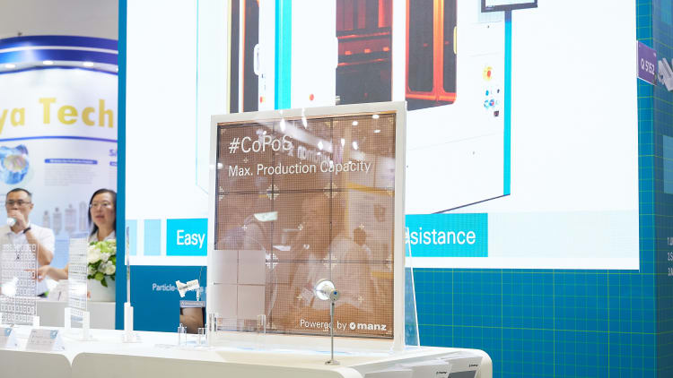
TSMC Teams Up with Ibiden and Innolux to Push CoPoS — Reportedly Flooring the Accelerator in Glass Substrates
To meet robust AI chip demand, TSMC is not only ramping CoWoS advanced packaging capacity but has, for the first time, disclosed progress on its "glass substrate" technology. The company further signaled that the next-generation advanced packaging battle is gradually shifting from CoWoS to CoPoS (Chip-on-Panel-on-Substrate), as it moves to build out a complete ecosystem ahead of the curve.
According to equipment-side sources, TSMC recently shared a "Glass Substrate Development for CoWoS" program with its supply chain. It has confirmed a partnership with ABF substrate giant Ibiden and panel maker Innolux to jointly validate the feasibility of introducing glass substrates into next-generation CoWoS advanced packaging. The aim is to address the warpage, thermal management, signal transmission, and power delivery challenges that loom over future large-die AI chip packaging.
At the same time, the move reflects rapidly intensifying customer demands around technical specifications and capacity, as well as mounting competitive pressure from Intel and Samsung Electronics. That pressure has finally pushed TSMC—long known for advancing R&D on a "cautious, not aggressive" basis—to step on the accelerator.
Glass substrates are viewed as a key technology for the "post-CoWoS era" thanks to their low warpage, low thermal expansion, high rigidity, and excellent signal and power-delivery characteristics. Supply chain sources say the three-way collaboration among TSMC, Ibiden, and Innolux, together with simulation validation, has shown that glass substrates can improve the package-warpage indicator COP (Chip on Package) by 16%, lower the effective coefficient of thermal expansion (Effective CTE) by 19%, and raise the effective modulus (Effective Modulus) by 31%.
On power integrity, resistance fell by 27% and inductance by 42%. Overall, introducing glass substrates can deliver a marked improvement in package performance (PKG Improvement).
TSMC nonetheless stressed that continued research and validation are still needed on glass thickness (Glass Thickness) and large-size CoWoS layout (Large-size CoWoS Layout). While full-scale mass production remains some distance away, this marks the first time TSMC has publicly disclosed joint glass-substrate validation results with Ibiden and Innolux—signaling that glass substrates have formally entered the industrialization-validation phase.
Industry observers added that the 16% COP improvement indicates package warpage is being effectively controlled. As AI GPU dies grow ever larger—with NVIDIA's GB200, GB300, and the now-ramping Rubin platform all expanding in package size—the importance of package flatness and warpage control has risen sharply. The performance glass substrates show in reducing warpage should help lift the yield and reliability of large packages.
In addition, the 19% reduction in SBT effective CTE shows improved matching between the glass material and the silicon die.
Today, silicon's CTE differs substantially from that of conventional organic substrates, making it prone to stress under temperature swings that can compromise package reliability. By contrast, glass has a CTE closer to that of silicon, which helps reduce thermal stress and mitigate cracking and solder-joint fatigue. The 31% gain in effective modulus means higher overall rigidity, providing better structural support. In particular, as HBM stack heights keep increasing, substrate rigidity is becoming a critical condition for supporting large packages.
The test sample TSMC used this time featured a 0.8mm glass core substrate, a package spec of 5x reticle CoW, and an overall package size of 85×110mm—an AI GPU package-class footprint. TSMC specifically emphasized "No SeWaRe (severe warpage) & Delamination," meaning no severe warpage or delamination/peeling—both yield killers—occurred during testing.
For glass substrates, material bonding reliability has always been a key challenge, so maintaining a stable structure at large package sizes demonstrates considerable progress in technical maturity.
Another focus of the program was the comparison between Glass-SBT and Organic-SBT. TSMC noted that Glass-SBT achieves "thin but better COP," whereas Organic-SBT shows "thick but worse COP"—glass substrates can stay thinner while simultaneously improving package flatness and reliability.
The partner roster also hints at the direction of the future supply chain.
Ibiden currently sits in the critical substrate supply chain for NVIDIA and AMD AI chips and is regarded as a key player in industrializing glass substrates. It previously announced a ¥500 billion investment to expand its new Ono plant in Gifu Prefecture, dedicated to high-end packaging substrates for AI servers—underscoring its strong ambitions in the AI advanced-packaging market. Innolux's inclusion on the partner list is likewise seen as an important step toward staking out the next-generation glass-substrate battlefield.
Industry sources say the biggest challenge for glass substrates is not the glass itself but Through Glass Via (TGV) technology. Because glass is fundamentally an insulator, tens of thousands of TGVs must be formed to create vertical conductive paths before signal and power transmission becomes possible.
Glass is also both hard and brittle, making it prone to micro-cracks during processing that can affect reliability and yield. As a result, via forming, copper-fill quality, and long-term thermal reliability are considered the three core hurdles to mass-producing glass substrates.
Separately, Intel began investing in glass-substrate R&D more than a decade ago and is regarded as the earliest and deepest player globally. Its glass-substrate pilot line in Arizona is gradually moving toward commercialization, and Intel is aiming to win AI GPU and ASIC customer orders through glass substrates and ultra-large chiplet packaging.
Samsung Electro-Mechanics (Semco) established a glass-substrate pilot line in 2025 and has set up a joint venture with Japan's Sumitomo Chemical group to build out a glass-substrate supply chain ahead of the market.
$TSM
35
36
279
36,444
Dracaena retweeted

Jun 15
China is Mogging Western Auto, and that’s Bad for Semis, National Security & War
If you live anywhere outside the US, you've noticed it: the streets are filling up with cars you've never seen before. Chery? Jaecoo? Zeekr? Leapmotor? BYD? No, you didn't miss a decade of car launches. They're Chinese. And they're everywhere. (1/10)🧵

30
38
306
63,894

This is an article that explains glass substrates in a very easy to understand yet detailed way.
I am confident it will be helpful not only from a technical perspective, but also from an investment standpoint.

2
14
107
21,790
Dracaena retweeted

Jun 12
Best FinX communities
- Finnish Tungsten Mafia
Absolute vibemaxxers. Stage 4 Asthma from chronic metal investing. Probably investing directly from their job at the coal mine. If you were ever in danger, 100 naked drunk men will turn up to your house to defend your honour. Brothers for life.
- Korean Leverage Degens
Severe mental illness. Their entire index moves like a 40k market cap shitcoin. Their only 2 options are Bill Hwang or homelessness. No fear of failure, as you can always max another credit card out. Beautiful people with a deep love for winner hard and losing even harder.
- Frenchies Cult of Paris
Their discord is the closest thing to a hedge fund. There is like 400 french adderal coke addicts doing dd simultaneously on 10000 different stocks at all times. Won't invest in anything that doesn't have a scent of Jean Paul Gaultier on it.
- Crypto Asylum Seekers
Watching them navigate a playing field where they can't rug you to zero is amazing to watch. 24-7 meme fest to cope with how downbad they've been for the last 6 months. No idea how to invest in an equity that actual has value, so they use Fibonacci TA on NVDA and Broadcom.
14
13
170
41,881
Dracaena retweeted

Jun 11
$AMD $INTC $ARM BOFA LIFTS CPU MARKET FORECAST ON AI DEMAND
Bank of America raised its 2030 server CPU total addressable market forecast to over $170 billion from $125 billion, citing agentic AI as a major demand driver. Analyst Vivek Arya said AI systems that plan and execute multi-step tasks will boost CPU usage alongside accelerators. BofA also raised price targets for AMD, ARM, and Intel, pointing to stronger long-term semiconductor growth and chip demand expansion.
44
51
343
79,870
Dracaena retweeted

Jun 11
Key takeaways on TSMC's next-generation advanced packaging, CoPoS (publicly available technical details omitted):
1. CoPoS is currently expected to enter mass production in 2H28. It is designed to improve the economics of ultra-large packages above the 9.5x reticle-size class, with NVIDIA’s Feynman AI chip a potential first adopter.
2. According to industry checks, glass is used in two distinct places (dimensions in mm):
→ 310 x 310 temporary glass carriers
→ 250 x 250 (pilot) / 510 x 515 (mass production) glass panels, processed and later cut into individual glass core substrates
3. The glass core substrate is essentially a three-layer structure: a glass core sandwiched between ABF (ABF-GCP) build-up layers on both sides. The widely discussed glass processing challenges, such as TGV formation and copper filling / metallization, are tied to this part of the stack.
4. Common misconceptions about CoPoS:
→ ❌ Misconception 1: CoPoS uses a glass interposer. ⭕️ Correction: The glass is not an interposer. The interconnect role is instead handled by the chip-side RDL, plus the TGV/Cu interconnects and ABF build-up layers in the glass-core substrate stack.
→ ❌ Misconception 2: Glass replaces ABF. ⭕️ Correction: As the substrate architecture above shows, glass and ABF coexist.
→ ❌ Misconception 3: Chips sit directly on glass. ⭕️ Correction: Chips are attached to the ABF build-up surface of the glass core substrate.
5. CoPoS should extend and reinforce TSMC’s leadership in advanced packaging, potentially giving that advantage visibility through around 2032.
36
135
786
565,895
Dracaena retweeted

Jun 9
Citigroup vient de publier une note sectorielle : l'écosystème Nvidia déclenche une révolution de l'AI factory, et la supply chain taïwanaise en sera le principal bénéficiaire au second semestre.
L'analyste semi de Citi identifie 3 tendances structurelles dans l'architecture des data centers AI :
1/passage au 800V HVDC pour l'alimentation des cabinets
2/Le refroidissement liquide comme standard incontournable, l'architecture disaggregée portée par la plateforme Vera Rubin de Nvidia
3/La montée en puissance du BMC comme cerveau de contrôle de l'infrastructure AI.
Chaque tendance pointe vers un fournisseur taïwanais : Foxconn/Delta/Auras/Aspeed
1
4
33
3,722
Dracaena retweeted

Jun 8
25년간 내리기만 했던 메모리 가격이 올랐다.
문제는.. 메모리를 수십 배 더 잡아먹는 Agentic AI 시대는 아직 오지도 않았다.

13
80
495
42,717
Dracaena retweeted

Jun 7
NPO is a much more sensible approach
Google and Huawei are adopting NPO first before transitioning to CPO
Jun 7

New conspiracy theory
90% not true.
Kyber mid-plane PCB is having yield issues due to infinite size and number of layers so Nvidia needs a backup plan, and CPO ain’t ready for prime time.
NPO is next best thing for full optical scale up
Probably totally wrong.
Do not take seriously.
7
6
167
39,374
Dracaena retweeted
Jun 7
메모리 슈퍼사이클이 곧 끝난다고 보는 뷰가 늘었다.
논리는 대충 이렇다.
하이퍼스케일러가 비싼 가격에 무한정 사주진 않을 것고, 중국 메모리 공급이 풀리고, 테라팹 같은 수직통합이 들어오면 2028 컨센서스가 무너진다는 것.
그래서 지금이 메모리 주식의 피크아웃이라고 본다.
일부는 맞는 말이고, 메모리가 사이클 산업이라는 본질은 변하지 않는다.
가격이 꺾이면 이익이 사라진다는 것도 변하지 않는다.
다만 베어 관점이 착각하는 한 가지 가정이 있다.
"효율화가 일어나면 수요가 줄어든다."
쉽게 말하면.. 메모리가 비싸지니까 빅테크가 안 살 것이고, 성능이 좋아지면 적게 사도 되니까 결국 수요가 감소한다는 시각.
그런데 역사적으로 보면 정반대였다.
효율화는 수요를 줄인 적이 없다.
항상 파이를 키웠다.
90년대 인터넷이 처음 깔릴 때.. 회선 속도가 빨라지자 무슨 일이 벌어졌나.
사람들이 인터넷을 적게 쓴 게 아니라 영상까지 보기 시작했다.
데이터 사용량이 곱셈으로 늘었다.
2000년대 모바일도 같았다.
통신 단가가 내려가자 사람들이 통화를 줄인 게 아니라 모바일 인터넷, 스트리밍, 영상통화를 같이 쓰기 시작했다.
클라우드도 마찬가지다.
컴퓨팅 단가가 내려가자 기업들이 서버를 안 산 게 아니라, 클라우드 위에 SaaS, 빅데이터, 머신러닝까지 올렸다.
경제학에는 이걸 부르는 이름이 있다.
제번스 역설.
자원의 효율이 좋아지면.. 자원 사용량이 줄어드는 게 아니라 오히려 늘어난다는 법칙이다.
19세기 영국에서 증기기관 효율이 좋아지자 석탄 소비가 줄지 않고 오히려 폭증했다는 데서 나온 개념이다.
이 법칙이 지금 AI에서 그대로 작동한다.
HBM3 - HBM3E - HBM4로 가면 대역폭이 1.5~2배씩 뛴다.
같은 GPU 한 대가 처리할 수 있는 토큰 수가 그만큼 늘어난다.
토큰당 비용이 내려간다는 뜻이다.
그렇다면 베어 시나리오대로 빅테크가 메모리를 덜 살까.
반대다.
토큰당 비용이 내려가면, 지금까지 AI 쓰기 비싸서 망설였던 곳들이 더 많이 들어오기 시작한다.
더 긴 컨텍스트, 더 복잡한 모델, 더 많은 사용자가 가능해지는 것이다.
시장 파이가 통째로 커진다.
추상적으로 들리니까 현장 얘기를 해보면,
처남이 램리서치 7년차다.
얼마 전 전화가 왔는데 사장이 직원들한테 2030년까지 자사주를 팔지 말라고 강조했다고 한다.
램리서치가 어떤 회사냐. 메모리 반도체 장비, 그중에서도 식각 증착 핵심 공급사다.
회사 사장이 직원한테 자사주를 2030년까지 들고 있으라고 따로 강조하는 건 그냥 던지는 말이 아니다.
회사 내부에서 보는 메모리 자본지출 사이클의 끝이 2030년보다 한참 뒤라는 신호다.
베어가 그리는 "2027~2028 피크아웃" 시점이랑 얘기가 다르다.
내 경험도 같다.
음악 관련 AI 플랫폼이랑 MOU 맺고 기업용 버전을 쓰고 있는데, 내년 연 사용료 예산을 또 올려야 한다.
업체가 직접 이유를 말했다.
"서버 운영비, 그러니까 토큰 사용량이 계속 늘어나서 데이터 사용료를 올릴 수밖에 없다"는 것이다.
다른 산업의 AI 플랫폼 쪽 사람들 얘기도 같다.
고객 기업이 새로운 AI 모델을 계속 요구하는데, 결국 가장 큰 문제가 서버 운영비라고.
이게 뭘 뜻하느냐...
AI를 이미 잘 쓰는 집단이 더 깊고 더 넓게 쓰고 있다는 것이다.
도입 단계의 수요 증가가 아니라, 정착 단계에서의 사용량 폭증이다.
한 번 AI를 업무에 쓰기 시작한 회사는 멈추지 않는다.
더 긴 컨텍스트, 더 많은 사용자, 더 복잡한 모델로 계속 확장한다.
제번스 역설이 현장에서 그대로 작동하는 모습이다.
AI 단위 비용이 내려갈수록 사용량은 줄어드는 게 아니라 곱셈으로 늘어난다.
그래서 메모리-GPU-전력 수요가 같이 곱셈으로 늘어난다.
그러니까 베어가 그리는 "비싸지면 빅테크가 안 산다"는 시나리오는 한 가지 핵심을 놓친 그림이다.
빅테크는 비싸도 산다.
안 사는 게 비합리적이라서가 아니라, 사는 게 더 합리적이라서다.
효율화가 토큰당 비용을 낮추고, 토큰당 비용이 낮아지면 AI 활용 범위가 더 커지고, 활용 범위가 커지면 또 더 많은 메모리가 필요해진다.
이것이 끊이지 않는 한 사이클이 끝나기 어렵다.
중국 공급 얘기도 한 단계 들어가야 한다.
CXMT가 DRAM 1위로 올라왔고 YMTC가 NAND 증설 중이라는 건 맞다.
그런데 중국이 들어오는 영역과 빅테크가 사는 영역이 다르다.
CXMT는 DDR4와 일부 DDR5 같은 범용 메모리에서 양산 중이다.
YMTC는 NAND다.
빅테크가 AI에 쓰는 건 HBM, 첨단 DDR5, LPDDR5X다.
이 두 영역 사이에 기술 갭이 상당히 크다.
CXMT가 HBM 양산까지 가려면 EUV 장비 제약, 1c 노드 수율, TSV 패키징... 다 미국 제재 라인 안에 묶여 있다.
최소 2~3년, 아마 5년 이상은 더 걸릴 것이다.
그래서 베어가 그린 "중국 공급 풀어 가격 붕괴" 시나리오는 범용 메모리에선 가능해도, HBM과 첨단 DRAM에선 2028까지 거의 영향 없다고 봐야 한다.
그리고 메모리가 그렇게 쉽게 만들어지는 기술이 아니다.
TSMC가 파운드리 생태계 만드는 데 30년 걸렸다.
SK하이닉스가 HBM에서 지금 자리 잡는 데 10년 넘게 걸렸다.
베어 관점에 묻고 싶은 게 하나 있다.
인터넷이 빨라졌을 때 데이터 사용량이 줄었나?
클라우드가 싸졌을 때 서버 수요가 줄었나?
스마트폰이 보편화됐을 때 통신 인프라 투자가 줄었나?
답은 다 똑같다.
효율화는 한 번도 시장 파이를 줄인 적이 없다.
항상 파이를 키웠다.
AI에서도 같다.
토큰당 비용이 내려갈수록 AI를 쓸 수 있는 산업이 늘고, 한 회사가 쓸 수 있는 범위가 늘고, 결국 더 많은 메모리가 필요해진다.
베어가 그린 "효율화 = 수요 감소" 등식은 역사적으로 한 번도 성립한 적 없다.
이번에도 다르지 않을 것이다.
106
467
2,423
788,370
Dracaena retweeted
Looks like I was right again panican.
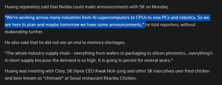
-Jensen “Demand is enormous. From wafers to silicon photonics and cable connectors, everything across the entire industry supply chain is in short supply.”
-"Nvidia CEO Huang, SK Chairman Chey to reveal cooperation plan Monday - Newsis
-"Nvidia CEO Jensen Huang: Memory shortage to continue for several years"
-"Nvidia CEO Jensen Huang: We might reveal some announcements tomorrow"

- Jensen is literally dancing on stage, signing tits and eating food on the floor
- Trump is telling you stocks should go up, not down
- Google is increasing capex
- Goldman Sachs and Morgan Stanley are giving 10x SpaceX revenue multiples
And you're BEARISH?
Serious answer:
We have 250 years of America. World cup. Mid-terms and Three $1T dollar IPO's. This all needs liquidity and high sentiment. The broligarch are all in coordination.
TSMC and Memory companies are systematically controlling the bubble. Despite Jensen pounding the drum for them to 3-4x capacity. (They deserve to be rich from this act)
Their plan - Demand stays higher than supply, prices stay strong, and they make great margins without betting the company. They'd rather sell out and raise prices than overbuild and risk a crash.
They've lived through this before. Memory especially has a long history of boom and bust, where someone overbuilds, the market floods, and everyone bleeds money.

6
11
108
25,721

Dracaena retweeted

Jun 3
STM is one of those companies that keeps showing up where you don’t expect it.
Look into SiC, it’s there. Look into GaN, it’s there. MEMS, STM32, robotics, satellites, data centers, automotive power — different themes on the surface, but the same company keeps appearing underneath.
My friend wrote a great anatomy of STM, not as a simple European auto semiconductor stock, but as a broad IDM platform sitting across the physical layers of AI infrastructure.
- The market buys STM under different labels: SiC, SpaceX, AWS, robotics, STM32, power semis.
- But the real question is simpler: how fast can this revenue cycle turn into margin recovery?
- STM’s edge is not one single theme, but the breadth of its portfolio across sensors, MCUs, power, RF, and optical communications.
Worth reading if you want to understand why STM keeps appearing across so many supposedly separate semiconductor stories.
5
10
74
13,386
La Commission européenne vient de présenter le Chips Act 2.0. C'est le texte de politique industrielle le plus ambitieux que l'Europe ait produit depuis le marché unique. Et il confirme, noir sur blanc, le changement de doctrine que Macron a annoncé Lundi à Versailles.
Comme promis, voici ce qu'il contient et pourquoi ça change la donne. Le post est long mais je vous résume un document de pratiquement 200 pages donc forcément ça ne se fait pas en 10 lignes.
----------------------------------
Le chips act 2.0 commence par poser le contexte :
- L'Union européenne produit moins de 10% des semi-conducteurs mondiaux.
- Le marché passe de 700 milliards de dollars en 2025 à 1 600 milliards en 2030.
- Trois hyperscalers américains contrôlent plus de 70% du cloud européen.
- La part des fournisseurs européens dans leur propre marché cloud stagne à 15% depuis 2022.
- l'UE dépense 264 milliards d'euros par an en logiciels et services IT propriétaires américains.
On y rappelle que le Chips Act 1.0, adopté en 2023, avait mobilisé 80 milliards d'euros d'investissements publics et privés.
Ce premier texte a montré ses faiblesse, le problème était que c'était un texte exclusivement supply-side.
On finance des usines.
On construit des fabs.
Mais sans clients garantis, sans mécanisme de commandes, sans préférence pour les produits européens il n'y a pas de client en aval et cela aboutit juste à une surcapacité, pas à la création d'une supply chain souveraine...
Le Chips Act 2.0 corrige le tir. Et la correction est radicale.
---------------------------------
Le pivot "demand-side". est donc le coeur du texte :
Le raisonnement est simple : On peut construire toutes les usines de puces qu'on veut sur le sol européen.
Si les clients industriels continuent d'acheter leurs composants à TSMC, Samsung ou aux fonderies chinoises, ces usines tourneront à vide. Le texte le dit explicitement.
"Demand-side weaknesses further undermine resilience. Fragmented markets, low volumes in key sectors, and limited procurement coordination reduce the commercial viability of European production."
Pour régler ça, le Chips Act 2.0 crée cinq mécanismes. Et c'est là que ça devient intéressant.
1️⃣ Le "Demand Forum."
C'est une plateforme officielle de mise en relation entre les fabricants de puces européens et les grands clients industriels : automobile, cloud, défense, énergie. L'objectif est de signer des contrats d'achat anticipé - des offtake agreements - avant même que les lignes de production ne tournent. En clair : au lieu de construire une usine et de prier pour trouver des clients, on verrouille les commandes d'abord. C'est exactement la logique qui a permis à Airbus de se construire face à Boeing. On ne lance pas un A320 sans carnet de commandes. Là, c'est pareil pour les puces.
2️⃣ Les "Demand Accelerators."
Des incitations financières pour que les industriels européens achètent des puces conçues ou fabriquées en Europe plutôt qu'importées d'Asie. Le texte va plus loin : il prévoit du co-design entre fabs et clients dès le début du cycle, bien avant la production de masse. Ça veut dire que le client participe à la conception du produit. C'est un changement fondamental. On passe d'une logique de catalogue - tu prends ce qu'il y a - à une logique de partenariat industriel sur mesure.
3️⃣ Les "Grand Challenges."
C'est le mécanisme qui me plaît le plus. L'UE finance des défis technologiques pour créer de la demande là où elle n'existe pas encore. Concrètement : l'Europe lance un appel à projet du type "concevez un processeur AI souverain pour les datacenters européens" et finance le développement. Ça génère de la demande structurelle avant même que les produits n'atteignent le marché. C'est exactement ce que font les Etats-Unis avec la DARPA depuis 60 ans. L'Europe n'avait jamais eu d'équivalent pour les semi-conducteurs. Maintenant c'est écrit dans la loi.
4️⃣ Le "Public Innovation Procurement."
Les administrations publiques européennes devront privilégier les technologies semi-conducteurs développées sur le sol européen. Le texte est explicite : "creating a clear and structured pathway to purchasing semiconductor technologies developed in the Union." Là encore, ce n'est pas du jamais vu dans le monde. Les Etats-Unis font exactement ça avec le Buy American Act depuis 1933. La Chine fait pareil. L'Europe était le seul bloc majeur à ne pas avoir de mécanisme de préférence pour ses propres technologies. C'est en train de changer.
5️⃣ La "Supply Chain Declaration" (PM10).
C'est la bombe discrète de la version finale, celle que personne n'a vue passer. Dans les marchés publics des secteurs critiques - défense, santé, télécom, énergie - les acheteurs publics peuvent désormais exiger une déclaration de provenance des semiconducteurs et utiliser le quota de fournisseurs domestiques comme critère d'attribution du marché. Ce n'est pas un Buy European Act formel. C'est un mécanisme facultatif. Mais c'est la première fois qu'un texte européen autorise officiellement l'origine des puces comme critère de sélection dans les marchés publics. Combiné aux niveaux de souveraineté cloud du CADA, ça crée un pipeline de commandes captives pour les composants conçus ou fabriqués en Europe.
Ce qu'il faut comprendre avec ces cinq mécanismes pris ensemble : pour la première fois, l'Europe ne se contente pas de financer l'offre. Elle organise la demande. Elle crée le client avant de créer l'usine. C'est un changement de paradigme complet par rapport au Chips Act 1.0 qui se résumait à "voici des subventions, construisez des fabs". Le problème du 1.0, c'est qu'on pouvait construire les plus belles usines du monde, si personne n'achète les puces qui en sortent, elles ferment. Le 2.0 ferme cette boucle.
C'est la traduction réglementaire exacte de ce que Macron appelle la "préférence européenne". Sauf que là, c'est un règlement de la Commission avec force de loi pour les 27 Etats membres.
--------------------------------------
Mais le pivot demand-side n'est qu'une partie du texte. L'autre partie, c'est ce que l'Europe prévoit de construire.
Et là, on entre dans du territoire inédit !
Le Chips Act 2.0 annonce la création d'une fonderie européenne sub-3 nanomètres. Open access. N'importe quel designer de puces européen pourra y faire fabriquer ses processeurs. Combinaison de fabrication avancée, d'intégration chiplets et de packaging 3D. Production pilote envisagée entre 2030 et 2033.
Coût estimé : 30 milliards d'euros, dont 15 milliards de fonds publics européens et nationaux.
Il faut mesurer ce que ça représente. Aujourd'hui, la part de marché européenne en fonderie pure-play est de 0,9%. Soit 0,8 milliard sur un marché mondial de 96 milliards. La part fabless est encore pire : moins de 1% des revenus mondiaux. 97% du chiffre d'affaires semi-conducteurs européen vient des IDMs : Infineon, STMicro, NXP mais pas de designers de puces.
Si une startup française ou allemande conçoit un processeur, elle est obligée d'aller chez TSMC à Taïwan pour le fabriquer. Il n'existe aucune fonderie en Europe capable de produire en dessous de 7 nanomètres.
Et la dépendance ne s'arrête pas à la fabrication : Le rapport d'impact détaille les maillons critiques de la chaîne.:
- L'ABF Film, le polymère isolant utilisé dans le packaging de chaque CPU et GPU au monde : Ajinomoto, un seul fabricant japonais, détient 95% du marché.
- Le T-Glass, le tissu de verre spécialisé pour les substrats AI : Nittobo, un autre japonais, à 90%.
- Les photoresists, les films chimiques indispensables à la lithographie : JSR et TOK, Japon, environ 90%.
- Le wafer dicing, la découpe des puces : DISCO, Japon, 86%.
- Les EUV mask blanks : AGC et HOYA, Japon, 93%.
Un conflit en mer de Chine, un tremblement de terre au Japon, et toute l'industrie européenne du numérique s'arrête. Le rapport d'impact de la Commission chiffre l'exposition : 1 530 milliards d'euros de production européenne dépendent directement de la disponibilité des semiconducteurs.
L'automobile seule pèse 934 milliards. Cette fonderie est une réponse à des dépendances mesurées, documentées, et concentrées sur un nombre dangereusement faible de fournisseurs.
-------------------------------------------------------
Le statut "First-Of-A-Kind" (FOAK) :
Pour que ce type de projet devienne réalité, il faut plus que de l'argent. Il faut de la vitesse. Et là, l'Europe partait avec un handicap majeur.
Construire une usine de semi-conducteurs en Europe prend en moyenne 7,5 mois de plus qu'en Asie. Rien que les permis. Et chaque année de retard coûte environ 5% du budget total du projet. Pour une fab à 20 milliards, ça représente 625 millions d'euros partis en fumée juste à cause de l'administration.
Le Chips Act 2.0 crée un statut spécial pour régler ça : le FOAK, "First-Of-A-Kind". Concrètement, si votre projet est le premier du genre en Europe, vous obtenez un traitement accéléré :
- Un seul guichet administratif par pays.
- 12 mois maximum pour obtenir tous les permis.
- Procédure entièrement numérique.
- Plus de navette entre cinq administrations différentes pendant trois ans.
Et l'évolution clé par rapport au Chips Act 1.0 ce qu'avant, ce statut ne couvrait que les usines de fabrication.
Maintenant il s'étend à toute la chaîne de valeur des semis conducteurs. Matériaux spéciaux, équipements, circuits imprimés, packaging avancé, assemblage, centres de design.
Si vous construisez quelque chose de nouveau dans l'écosystème semi-conducteurs européen, vous pouvez en bénéficier.
C'est la "méthode Notre-Dame" de Macron transposée au niveau européen pour l'industrie des semi-conducteurs.
-------------------------------------------------------
Les "Régions d'Excellence" :
Jusqu'ici, chaque pays européen essayait d'attirer les investissements semi-conducteurs dans son coin. La France poussait Grenoble, l'Allemagne poussait Dresde, les Pays-Bas poussaient Eindhoven. Résultat : de la concurrence intra-européenne au lieu de la coordination. Le Chips Act 2.0 change ça.
Le texte crée un label officiel "European Semiconductor Region of Excellence". Les régions labellisées bénéficient d'investissements coordonnés en énergie, en réseau électrique, en formation et en attractivité. Concrètement : si vous êtes un investisseur et que vous cherchez où implanter une activité semi-conducteurs en Europe, ces régions auront l'infrastructure électrique dimensionnée, les talents formés, les permis accélérés et les connexions avec le reste de l'écosystème.
Les candidats évidents :
- Dresde en Allemagne (déjà surnommée "Silicon Saxony")
- Grenoble en France (STMicro, Soitec, CEA-Leti)
- Eindhoven aux Pays-Bas (ASML, NXP)
- Leuven en Belgique (imec)
- Catane en Italie (STMicro SiC)
- Villach en Autriche (Infineon).
L'idée de fond est simple : plutôt que de voir 27 pays se battre pour attirer une fab, on structure l'écosystème à l'échelle du continent. Chaque région a sa spécialité. Les régions se renforcent mutuellement. C'est la logique du réseau, pas de la compétition.
On voit ainsi une véritable volonté de mutualiser les efforts plutôt que de laisser chaque pays jouer perso.
------------------------------------------
Le Chips Act 2.0 n'arrive pas seul :
Il fait partie d'un package de quatre textes déposés le même jour par la Commission. Et c'est quand on les lit ensemble que l'on comprend la stratégie.
Le CADA (Cloud and AI Development Act) impose de tripler la capacité datacenter européenne en cinq à sept ans. 200 milliards d'euros d'investissements.
Il crée quatre niveaux de souveraineté pour les services cloud, et les niveaux les plus élevés exigent une chaîne d'approvisionnement hardware traçable en Europe. Le lien est explicite dans le texte : "CADA's measures to accelerate the deployment of data centre infrastructure acts as a demand-side measure for the Chips Act 2.0."
En clair : chaque datacenter construit en Europe devient un client pour les puces européennes. Le CADA crée la demande. Le Chips Act crée l'offre. Les deux textes se nourrissent mutuellement.
L'Open Source Strategy consacre RISC-V comme architecture souveraine pour les semi-conducteurs européens. Et là, il faut comprendre pourquoi c'est un sujet aussi important.
Aujourd'hui, quasiment tous les processeurs du monde utilisent une architecture propriétaire : ARM (contrôlé par SoftBank, Japon) ou x86 (Intel et AMD, Etats-Unis). Chaque puce qui utilise ces architectures paie une licence. Et surtout, elle dépend d'une autorisation étrangère pour exister. Si demain les Etats-Unis décident de restreindre l'accès à ARM ou x86 comme ils l'ont fait avec Huawei, l'Europe n'a aucune alternative. Sauf si elle en construit une.
RISC-V est cette alternative. C'est une architecture open source, libre de droits, que n'importe qui peut utiliser et modifier. Et l'Europe est en train de bâtir tout un écosystème dessus.
- Le programme EPI (European Processor Initiative) développe deux pistes en parallèle : SiPearl conçoit le processeur Rhea pour les supercalculateurs européens, pendant que le Barcelona Supercomputing Center développe les accélérateurs EPAC entièrement basés sur RISC-V.
- Le projet DARE (Digital Autonomy with RISC-V in Europe) fédère des dizaines d'acteurs pour créer un écosystème logiciel complet autour de cette architecture.
- Kalray conçoit des processeurs de traitement de données (DPU).
- 2CRSi les intègre dans des serveurs souverains et coordonne le consortium AETHER pour les AI Gigafactories européennes. SiPearl fournit les processeurs HPC.
- Bull (racheté par l'Etat français) fabrique les supercalculateurs.
L'enveloppe prévue par la Commission pour l'écosystème RISC-V et les outils EDA open source : 1 milliard d'euros sur sept ans.
La Roadmap Energie/AI, quatrième texte du package, fixe les standards de durabilité pour les datacenters et organise l'accès au réseau électrique pour les futures AI Gigafactories.
Au total, les quatre textes forment une boucle :
- Le CADA crée la demande de datacenters.
- Les datacenters ont besoin de puces.
- Le Chips Act finance la production des puces.
- L'Open Source Strategy fournit l'architecture libre.
- La Roadmap Energie garantit l'alimentation.
C'est une véritable politique industrielle intégrée à tout les niveaux de la chaine de valeur des semi-conducteurs.
-------------------------------------------------
Deux ajouts stratégiques : la photonique & le quantique
La photonique intégrée est ajoutée comme sixième composante officielle du Chips for Europe Initiative. Les circuits photoniques intégrés (PIC) sont la couche d'interconnexion optique qui permet aux datacenters IA de fonctionner à grande échelle. Le cuivre ne suffit plus. L'Europe dispose d'un avantage réel sur ce segment grâce à imec, au CEA-Leti et à plusieurs fonderies spécialisées.
Le quantique reste comme composante du Pilier I avec un pont explicite vers un futur Quantum Act européen. Le texte précise que la cohérence entre les deux textes "fournira l'opportunité d'établir un cadre politique quantique européen complet". Le renouvellement de la stratégie quantique que Macron a évoqué lundi à Versailles s'inscrit dans cette trajectoire.
Et une précision importante pour ceux qui pensent que l'Europe part de zéro. Le rapport d'impact documente les positions de force européennes dans la chaîne de valeur :
- ASML détient 100% du marché mondial de la lithographie EUV et 92% de la lithographie totale.
- Siemens EDA est le troisième éditeur mondial d'outils de conception de puces (15% de part de marché).
- Merck et Air Liquide contrôlent plus de 50% du marché mondial des précurseurs ALD et CVD, les molécules qui permettent de déposer les couches atomiques dans les puces avancées.
- Wacker Chemie est le leader mondial du polysilicium electronic-grade, la matière première des wafers.
- ASM International détient 10% du marché mondial de l'ALD, la technique de dépôt la plus critique pour les noeuds avancés.
- BESI détient 43% du marché mondial du die attach, l'étape d'assemblage des puces.
- Soitec est nommé dans le rapport comme acteur clé des wafers SOI et epiwafers.
etc..
L'Europe n'est pas absente de la chaîne de valeur. Elle est dominante sur certains maillons critiques (lithographie, chimie, substrats) mais absente ou marginale sur d'autres (fonderie, design fabless, packaging). Le Chips Act 2.0 n'invente pas un écosystème. Il coordonne des forces existantes et comble les trous.
-------------------------------
Quand on met tout ça bout à bout, voici ce qui vient de se passer en 72 heures :
Lundi 01 juin, Macron dit à Versailles devant les investisseurs étrangers : "L'Europe a peut-être été trop naïve jusqu'à présent." Il annonce la préférence européenne, la clause de protection, le fast-track pour les data centers, le renouvellement quantique.
Mercredi 03 juin, la Commission européenne dépose un texte qui crée des mécanismes contraignants pour forcer la demande de puces européennes, qui prévoit une fonderie sub-3nm ouverte à tous les designers EU, qui impose un guichet unique à 12 mois, qui lie chaque datacenter à la consommation de composants européens et qui structure l'écosystème en régions d'excellence.
Et dans les 173 pages du rapport d'impact publié le même jour, un mécanisme discret mais décisif : la Supply Chain Declaration dans les marchés publics, qui permet pour la première fois d'utiliser l'origine européenne des puces comme critère d'attribution.
Le discours et la loi disent la même chose. La différence c'est que le discours s'évapore. La loi reste.
-------------------------------
Depuis aujourd'hui, le changement de doctrine européenne n'est plus une intention. C'est un cadre réglementaire contraiganant pour 27 Etats, 450 millions de citoyens et un marché semi-conducteurs qui pèsera 1 600 milliards de dollars en 2030.
"L'Europe n'est plus naïve." 🇪🇺
Merci de m'avoir lu.
Firisis
31
39
193
21,124
Dracaena retweeted

Jun 3
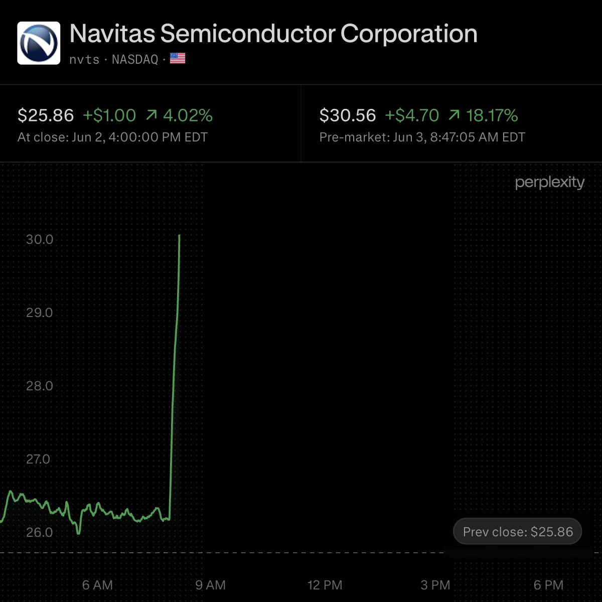
$NVTS showcased its 800V-to-6V DC-DC power delivery board at NVIDIA’s AI Factory MGX ecosystem event during Computex.
The board uses 16 GaNFast FETs and targets 97.5% peak efficiency, 1 MHz switching, and 2100 W/in³ power density.
Navitas says the design removes the need for a traditional 48V intermediate bus converter inside compute server trays, helping enable smaller and denser AI server power systems.
10
45
320
51,136

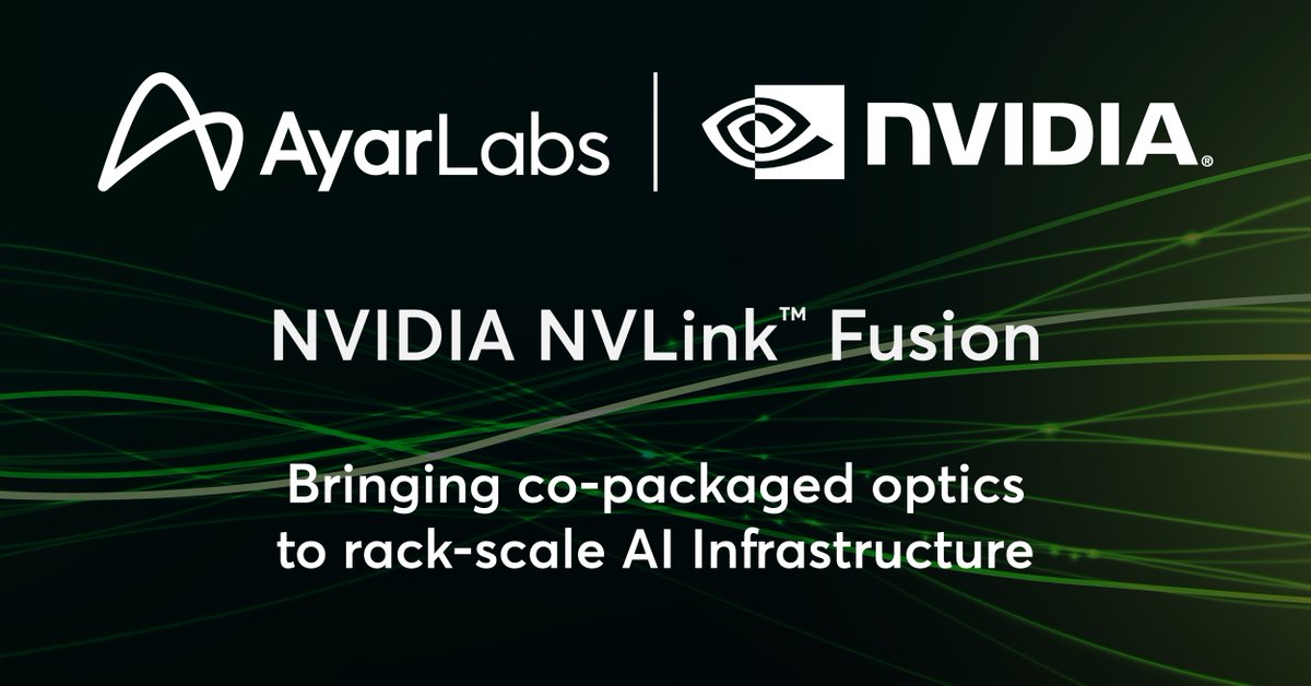
Today, @AyarLabs announced it has joined the @nvidia NVLink Fusion ecosystem, introducing co-packaged optics as a foundational building block for hyperscalers and system innovators deploying heterogeneous compute in NVIDIA AI factories.
Press Release:
bit.ly/4oa8epa
32
100
757
616,956
Dracaena retweeted
Jun 2
🫡🫡🫡🫡🫡

Just to prepare you guys, this Google raise means memory is going way higher.
3
8
309
39,980
Dracaena retweeted

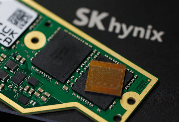
Jun 2
SK hynix just said AI memory demand is now so large that it will double wafer capacity within 5 years, yet still expects supply to stay tight until 2030.
A wafer is the round silicon starting plate that becomes thousands of memory chips, so doubling wafer capacity basically means SK hynix is trying to expand the physical base of its chip output, not just run current lines harder.
AI supply is increasingly constrained by the physical rhythm of memory manufacturing, where wafers, packaging, yields, and supply agreements move far slower than GPU roadmaps.
The pressure comes from HBM (High-bandwidth memor), the stacked memory used beside Nvidia GPUs.
HBM is hard to scale because it needs advanced DRAM, stacking, packaging, testing, and close work with GPU designers, which is why SK hynix is working with Nvidia and TSMC on HBM4 base dies.
---
The global memory market.
The global memory market has 2 main layers: DRAM, which includes the memory used next to CPUs and AI GPUs, and NAND flash, which is the storage inside SSDs, phones, and data centers.
In DRAM, the market is extremely concentrated, with Samsung at 38.5%, SK hynix at 28.8%, and Micron at 22.4% in 1Q26, meaning the top 3 control about 90% of global DRAM revenue.
In HBM, which is a premium submarket inside DRAM, the AI-specific memory used beside Nvidia GPUs, SK hynix is the market leader, with 58% share in 1Q26, while Samsung and Micron each had 21%.
HBM, or High Bandwidth Memory, is a special form of DRAM built for extreme data movement.
The difference is physical design.
Normal DRAM chips usually sit on memory modules or near the processor, and data moves through relatively narrower connections.
HBM stacks multiple DRAM dies vertically and places them very close to the GPU through advanced packaging, which creates a much wider data path.
That wider path gives AI chips much higher memory bandwidth, meaning the GPU can receive data faster instead of sitting idle.
8
43
225
17,803