
🛠️ Industrial Integrity & Validation Audit
1. Covalent Bonding (Beyond Delamination) Zero mechanical stress. Implementation of Plasma Functionalization (Oxford/PlasmaEtch standards) to create chemical anchoring sites. We achieve Molecular CTE Synchronization between the Nitinol-S matrix and the Graphene basal plane. This is atomic integration, not a coating.
2. Extreme Thermal Management 🌡️
Graphene basal plane thermal conductivity: 5,000 \text{ W/mK} (Validated by Graphenea). By surpassing the Fourier limit of copper, we redistribute thermal loads in milliseconds, ensuring the structural integrity of the silver encapsulation under extreme ΔT.
3. \lambda/20 Precision Optics 🛰️
Ag-999 PVD encapsulation designed to neutralize Atomic Oxygen (AO) erosion in LEO. Reflectivity protocol: JWST Grade (Northrop Grumman/Ball Aerospace). High-fidelity optical performance without the mass or brittleness of Beryllium.
4. Solid-State Actuators ⚡
"The Best Part is No Part". Utilizing NASA Glenn SMA protocols, the Nitinol-S matrix functions as a structural nerve. 40% mass reduction by eliminating mechanical gears, motors, and parasitic wiring.
🌐 Ecosystem Synthesis:
Architecture optimized through validated standards:
NASA Glenn (SMA Structural Dynamics)
Oxford Instruments (Plasma Functionalization)
Northrop Grumman (Space-Grade Optics)
The physics is settled. Scaling is logistics.
#SpaceX #Tesla #Starship #MaterialScience #GenesisArchitecture #FirstPrinciples #Anduril @omead @lrocket @tomzhu_nz @ckuehmann @elonmusk

1
90

6 Nov 2025
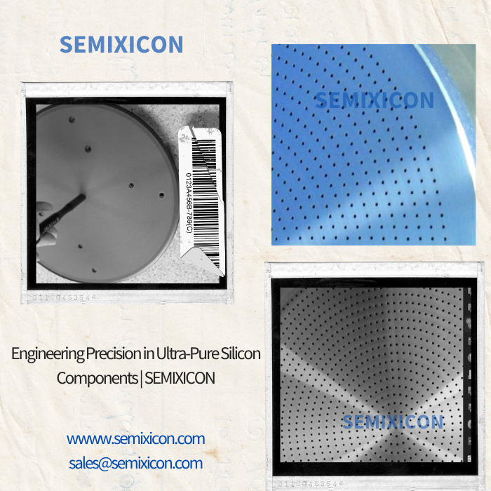
Ultra-Pure Silicon Components | SEMIXICON
Purity:>99.9999%(6N ) semixicon.com #SiliconSpares #EtchComponents #FocusRing #SputteringTarget #300mmWafer #200mmWafer #PVD #PlasmaEtch #SemiconductorMaterials #HighPuritySilicon #PolySilicon #MonoSilicon #CVD #ChamberComponent
3
13
3 Sep 2025
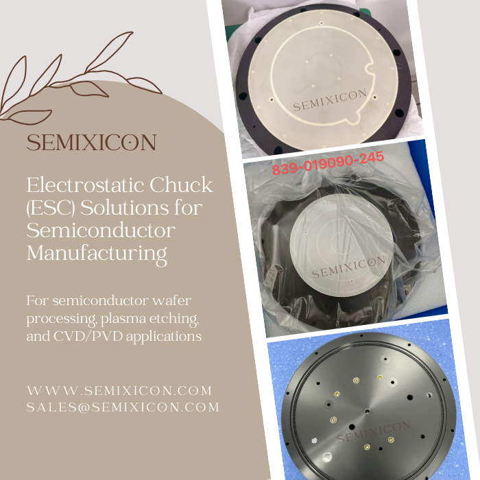
SEMIXICON –Electrostatic Chuck (ESC) Solutions for Semiconductor Manufacturing
semixicon.com
#LAMESC #ElectrostaticChuck #ECHUCK #ESCrefurbishing #ESCreconditioning #ESCnewmake #ESCnewdesign #semiconductorchuckrepair #LAMspareparts #AMATspareparts #ESCrepair #plasmaetch
2
28

10 Jul 2025
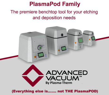
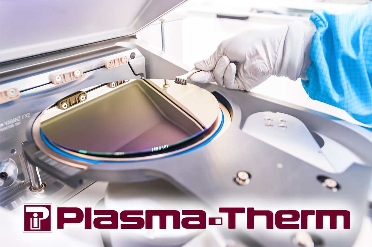
Spotlight on #AdvancedVacuum — a legacy Plasma-Therm brand driving innovation with platforms like Vision & PlasmaPODs. High-performance, flexible solutions backed by trusted quality. Learn more: hubs.la/Q03wGZL50
#PlasmaTherm #PlasmaPOD #VisionSystem #PlasmaEtch #PlasmaDep
2
307

27 Jun 2024
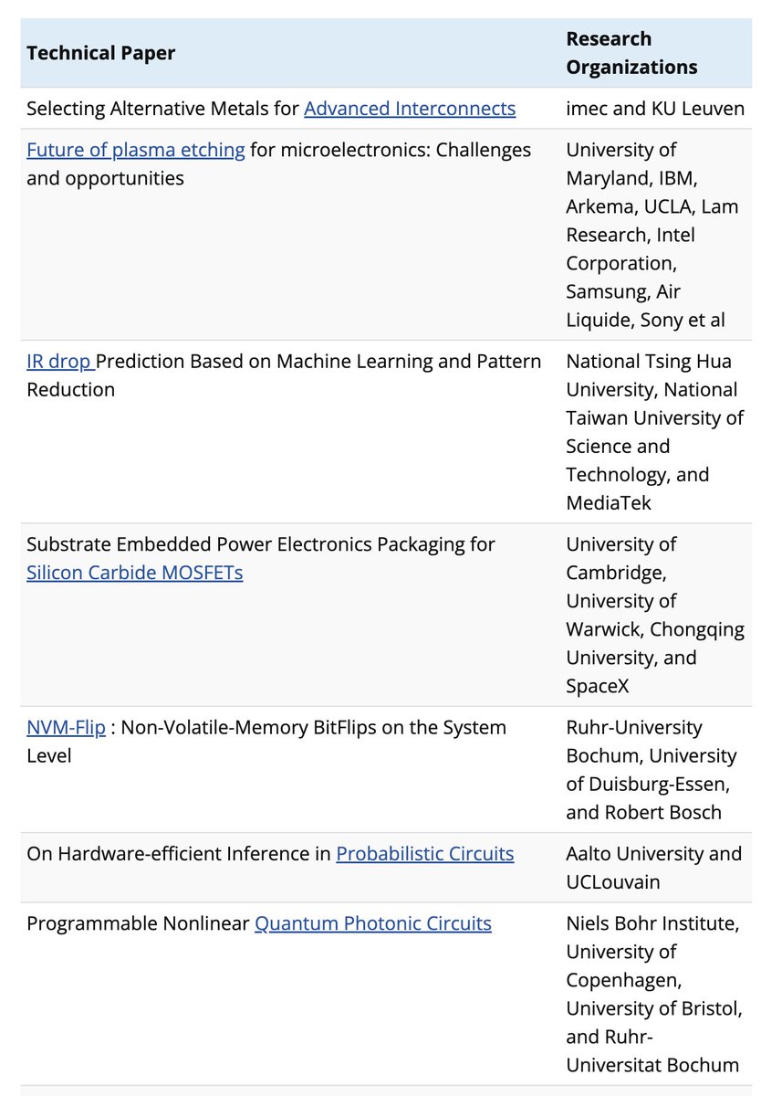
New technical papers recently added to Semiconductor Engineering’s library.
semiengineering.com/chip-ind…
#semiconductor #interconnnects #plasmaetch #IRdrop #semiEDA #MOSFETs #NVM #Quantum
#photonics #semiEDA
5
677

25 Jun 2024
New technical papers recently added to Semiconductor Engineering’s library. semiengineering.com/chip-ind…
#semiconductor #interconnects #plasmaetch #IRdrop #semiEDA #SiC #NVM #hardwaresecurity
#quantum #photonics

1
6
296

9 Feb 2023
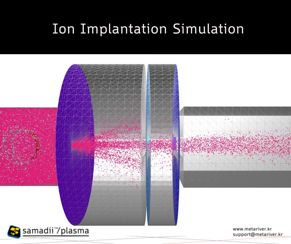
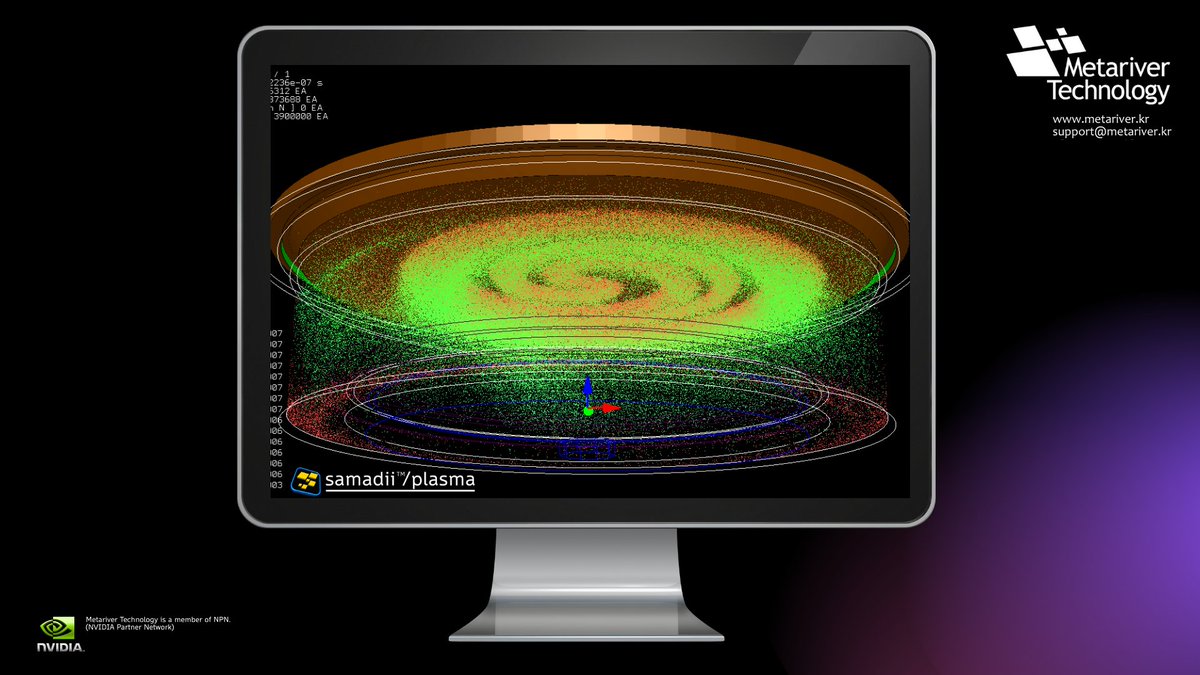
Run faster & more realistic #plasma #simulations in less time with our #GPU accelerated #plasma #Simulation software #samadii/plasma, contact us at support@metariver.kr
#RF #sputtering #etching #antenna #electronics #displays #multiphysics #PlasmaEtch #OLED #semiconductor #cvd
2
459
5 Jan 2023
#Simulation of #ICP (Inductively coupled #plasma)using #samadii/plasma, you can appreciate & you can appreciate the #ion behavior,Ion #density & the processing rate on the #substrate
#RF #antennas #ICP #GPU #electronics #displays #PlasmaEtch #semiconductor #semiconductors #wafers
2
180
15 Sep 2022
Learn more about our #plasma simulation & #modeling software #samadii/plasma👉 youtu.be/lCCey__fPSY
#simulation #Electronics #etching #cuda #multiphysics #PlasmaProcess #PlasmaEtch #PlasmaEtching #sputtering #semiconductors #semiconductor #display #chip #nvidia #antennas #OLED
2
6 Sep 2022
ICP #Simulation is used in industries such as #thinfilms #semiconductors & liquid crystal #displays Watch👉 lnkd.in/db2Gt-p8
#PLASMA #ICP #Electronics #etcher #cuda #deposition #etching #multiphysics #PlasmaProcess #PlasmaChamber #PlasmaEtch #PlasmaEtching #gpu #wafer
2

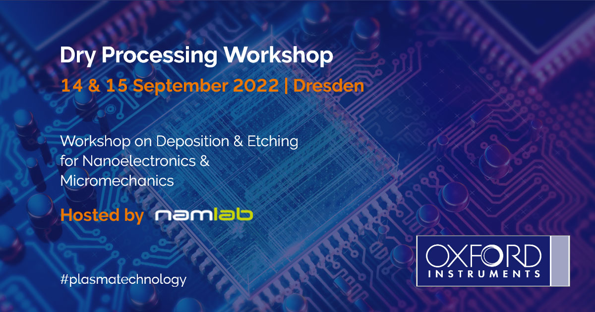
5 Sep 2022
Few days left to purchase the ticket for the 𝗗𝗿𝘆 𝗣𝗿𝗼𝗰𝗲𝘀𝘀𝗶𝗻𝗴 𝗪𝗼𝗿𝗸𝘀𝗵𝗼𝗽 in Dresden. Meet with 11 experts to discover more about #plasmaetch and #plasmadeposition processes. Register your interest.
okt.to/yl3u7P
#plasmatechnology
1
3
16 Aug 2022
One month is left for the Dry Processing Workshop at the NaMLab facility in Dresden. There will be a lot of topics dedicated to #plasmaetch and #plasmadeposition processes. You can check the agenda here:
okt.to/QaUVpr
#plasmatechnology

1
4

11 Jul 2022
Come visit Samco at Semicon West Booth 1533.
We will introduce New plasma etch cluster tools and ALD equipment.
#Plasma #Etch #PlasmaEtch #PECVD #ALDep #CVDep #semiconductor
samco.co.jp/en/events/2022/s…

2

6 Apr 2022
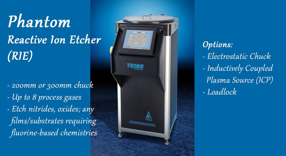
#TrionTechnology will be at SEMICON WEST 2022 Booth 745. See you there! conta.cc/3jc4Jh7 #semiconwest2022 #semiconwest #semi #reactiveionetch #plasmaetch #RIE #inductivelycoupledplasma #SiO2Etch #Si3N4Etch
3
31 Mar 2022
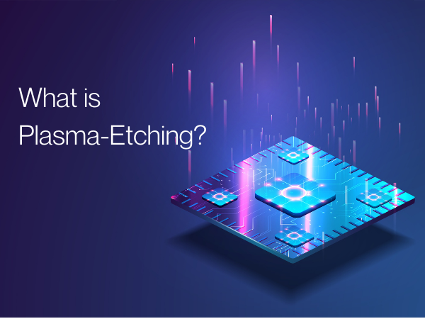
Have you heard of plasma etching?
Plasma etching ("dry" etching) is a plasma-based process that facilitates the removal of material from the surface of a substrate. #LearnMoreHere
#PlasmaEtch #NanoTechnology #Semiconductor
Plasma-Therm: Etch hubs.la/Q016nl9_0
ALT Plasma-therm
2
31 Mar 2022
#samadii-Plasma visualizes the #plasma process through #ion & #electron #particle behavior.
#Simulation #sputtering #ionimplantation #etching #plasma #PlasmaProcess #PlasmaChamber #PlasmaEtch #PlasmaEtching #Etch #semiconductors #semiconductor #wafer #LED #OLED #display #sensors
2
30 Mar 2022
Looking into products at Plasma-Therm? Check out our process equipment:
hubs.la/Q016nlbR0
#PlasmaEtch #IonBeamEtch #DeepSiliconEtch #Semiconductor
2
14 Feb 2022
Have you heard of plasma etching?
Plasma etching ("dry" etching) is a plasma-based process that facilitates the removal of material from the surface of a substrate.
#Semiconductor #PlasmaEtch #IonBeamEtching
hubs.la/Q013KNTx0

2
2 Feb 2022
What is plasma etching? Plasma etching ("dry" etching) is a plasma-based process that facilitates the removal of material from the surface of a substrate. Learn more by clicking below!
#PlasmaEtch #PlasmaTherm #ICPRIE #ICP #RIE #ReactiveIonEtch #IonEtch
hubs.la/Q012SCZk0
1

13 Dec 2021
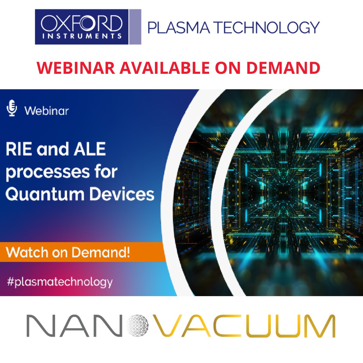
Watch on demand the Oxford Instruments Plasma Technology Webinar on RIE and ALE Processes for Quantum Devices.
Find details in link below:
bit.ly/3EUnRte
#2Dmaterials #plasmaetch #photonics #nanofluidics #spintronics #quantumcomputing #nanovacuum #nanofabrication
1
2