
@logly が広告代理店向けAI広告プラットフォームを発表
𝙍𝙚𝙖𝙙 𝙈𝙤𝙧𝙚: itbusinesstoday.com/martech/…
#AdTechnology #Advertising #ClaudeCode #GenerationAI #Logly
7

Die sind bereit mehr zu zahlen und achte. weniger auf den Preis. Bei AdTechnology war dies eines der ersten Targetringkriterien,die wir damals (vor ca. 20 J) gebaut hatten.
1
2
305


Apr 23
Des ex-ingénieurs ASML lancent une puce AI qui consomme 100x moins que Nvidia
Euclyd a été fondée en 2024 par un ancien directeur d'ASML. Siège sur le High Tech Campus d'Eindhoven, le même écosystème qui a produit ASML, NXP et Philips.
L'équipe compte parmi ses advisors Peter Wennink, ex-CEO d'ASML, et Federico Faggin, l'inventeur du premier cpu Intel.
Leur produit s'appelle CRAFTWERK. C'est un System-in-Package conçu uniquement pour l'inférence.
Les GPU classiques perdent énormément d’énergie à faire voyager les données entre la mémoire et les processeurs.
CRAFTWERK utilise une architecture dataflow qui minimise ces déplacements inutiles en gardant les données tout près des calculs.
La grande spécificité est l’UBM (Ultra Bandwidth Memory) : 1 To de mémoire DRAM directement intégrée sur un énorme interposer silicium, offrant une bande passante extrême (jusqu’à 8 000 TB/s) pour rendre l’inférence beaucoup plus économe en énergie.
La revendication : jusqu'à 100x moins de consommation par token d'inférence par rapport aux dernières générations Nvidia. C'est une déclaration en simulation, pas encore validé en production réelle.
L'inférence devient le poste de dépense dominant dans les data centers à mesure que les agents IA se multiplient. Un gain réel de 10x suffirait à créer un marché.
En novembre 2025, Euclyd a signé un partenariat avec ADTechnology, le plus grand design house coréen, pour porter CRAFTWERK sur silicium. La fabrication passera probablement par TSMC.
Startup pas encore coté.

4
51
259
27,419

Panie Dr, wypowie Pan kiedyś słowa przed kamerą, że takie firmy jak ADtechnology czekają na zlecenia produkcyjne a uradujesz Pan obserwatora jeszcze sprzed pierwszej książki. (Mam z autografem).
Takie rzeczy robimy.
ad-technology.pl/realizacje/
8
8
130
16,338


Samsung Electronics Foundry Strikes Back, Begins Mass Production of ‘Exynos 2600’
Samsung Electronics has begun mass production of its next-generation application processor (AP), the Exynos 2600. The chip is expected to be installed in the standard model of the Galaxy S26, scheduled for release early next year by Samsung’s Mobile eXperience (MX) division.
What stands out is that Samsung started mass production earlier than expected. Since the Exynos 2600 is the first product using the SF2 (1st-generation 2nm) process, Samsung appears to have taken the initiative to ensure performance stability by beginning production ahead of schedule.
According to industry sources on the 29th, Samsung recently began wafer input for the Exynos 2600. The chip is expected to be fab-out between late October and early November. Fab-out refers to the stage when wafer front-end processing is completed, and the wafer exits the fab.
The Exynos 2600 will be manufactured using the SF2 process, Samsung’s most advanced node. This process applies Samsung’s 3rd-generation Gate-All-Around (GAA) technology. Compared to the previous SF3, performance has improved by 12%, and power efficiency by 25%.
After fab-out, the chips will undergo wafer testing, packaging, and package testing. Wafer testing is outsourced to partners, while packaging and subsequent steps are handled internally at Samsung.
With the Exynos 2600 now in mass production, its inclusion in the Galaxy S26 is virtually confirmed. While the final AP allocation has not been officially decided, based on past patterns, the Exynos 2600 is expected to be used in domestic and European models, while Qualcomm Snapdragon APs will power the North American and Chinese models.
The decision to start production in September appears to reflect better-than-expected yield improvements. Samsung’s SF2 process yield was around 30% in Q1 this year but has reportedly climbed to around 50%. However, this yield figure is AP-specific and may vary depending on die size.
Previously, Samsung suffered significant losses in its System LSI and Foundry businesses when it failed to equip the Galaxy S25 with the Exynos 2500. To recover, the company has devoted greater resources to the development and mass production of the Exynos 2600.
If Samsung succeeds with this project, it could strengthen its position in the leading-edge foundry market. TSMC continues to hold a near-monopoly but faces rising costs and capacity limitations, pushing more customers to seek alternatives.
One such customer is Tesla, which recently signed a $16.5 billion foundry contract with Samsung. Tesla plans to manufacture its AI6 system semiconductor using Samsung’s SF2P (2nd-generation 2nm) process.
Other companies, such as Japanese AI unicorn Preferred Networks (PFN), Ambarella, and ADTechnology, are also developing chips on Samsung’s 2nm node.
A Samsung Foundry partner commented:
“The mass production of Exynos 2600 is a crucial project not only for Samsung but also for its partners. The outcome will determine Samsung Foundry’s ability to attract clients and secure orders going forward. Given Samsung’s long-node strategy for 2nm, continuous process improvement can be expected.”
6
6
63
21,111

根據ZDNet KOREA的報導,業界人士指出,三星晶圓代工事業部正積極在全球市場爭取SF2P製程的客戶訂單。SF2P是三星2奈米製程下一代製程技術,計劃於2026年進入量產階段。與2025年下半年預計量產的第一代2奈米(SF2)製程相比,SF2P在性能上提升了12%,功耗降低了25%,晶片面積也縮小了約8%。目前,SF2P的晶片設計基礎,包括設計套件 (PDK) 已初步完成,三星也正積極向國內外大型科技公司及IC設計公司推廣其製程代工服務。
日前,電動車大廠特斯拉已與三星於上個月簽訂了一份價值高達22兆韓圜(約 160 億美元)的半導體代工合約。這項合作的重點是為特斯拉生產名為「AI6」的高性能系統半導體,該晶片將廣泛應用於特斯拉的下一代全自動駕駛(FSD)系統、機器人技術以及資料中心等領域。
消息指出,AI6晶片已確定採用三星電子的SF2P製程。三星計劃初期將在韓國的晶圓代工與封裝設施中生產AI6晶片的初次樣品,隨後將在美國德州泰勒市新建的晶圓代工廠進行大規模量產。而泰勒市晶圓廠的生產設備裝機將於2025年底啟動,並預計從2026年開始進入量產階段。
而除了特斯拉,許多以擴展AI半導體為主要業務的韓國本土IC設計公司也對SF2P製程表現出濃厚興趣。本月中旬,韓國DeepX公司宣布將與三星晶圓代工,及設計解決方案合作夥伴(DSP)Gaonchips攜手,共同開發下一代生成式AI半導體DX-M2。
報導指出,DX-M2也將以SF2P製程為基礎。按照計畫,DX-M2預計於2026年上半年完成MPW 多晶圓試產,並有望於2027年進入大規模量產。此外,三星電子與ADTechnology、Arm,以及Rebellions合作開發的下一代AI運算小晶片平台,同樣也將採用SF2P製程。
報導引用韓國半導體業界相關人士的分析指出,SF2P製程的成功與否,關係到三星電子在先進晶圓代工領域的競爭力。這項製程不僅是客戶的關鍵技術,也與三星自家Exynos系列的行動應用處理器有著密切關聯。儘管SF2P的良率目前尚未完全穩定,但透過持續的研發投入與優化,三星預計將在2025年下半年實現顯著的技術成熟和良率提升。

1
1
27
6,280
Report: Samsung Foundry's '2nd Generation 2nm' Process Full Steam Ahead... First Step in Securing External Customers
Samsung Electronics has begun preparations to restore its next-generation foundry competitiveness. The company recently completed the basic design for its 2nd generation 2nm (SF2P) process and has started promotions with partners to attract customers.
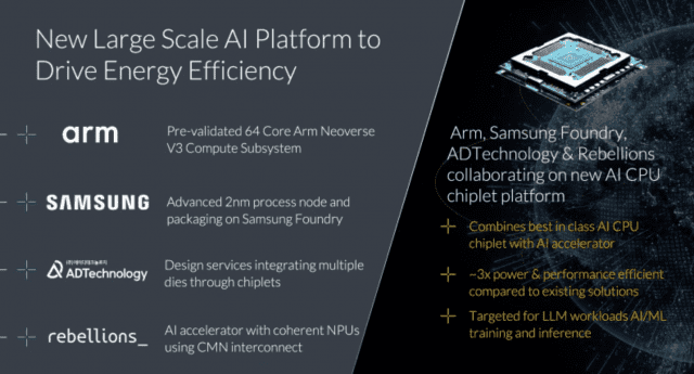
It has been confirmed that the next-generation AI computing chiplet platform, which Samsung Electronics announced last year it would co-develop with ADTechnology, Arm, and Rebellions, recently adopted the SF2P process. This marks its first application beyond the internal customer, System LSI's next-generation mobile AP (Application Processor).
According to industry sources on the 27th, Samsung Electronics Foundry and Design House (DSP) companies have recently begun full-scale promotions for the SF2P process.
SF2P Process, External Customer Attraction Preparations Complete... Design Kit Also Nearing Completion
SF2P is Samsung Electronics' 2nd generation 2nm process, targeting mass production next year. Samsung Electronics explains that compared to the 1st generation 2nm (SF2) process, which is scheduled for mass production in the second half of this year, SF2P offers a 12% performance improvement, 25% reduction in power consumption, and 8% smaller area.
In the meantime, Samsung Electronics and its DSP partners have been conducting groundwork with potential customers for SF2P process orders. They are also preparing for the design and mass production of the next-generation mobile AP based on the SF2P process with their internal customer, System LSI.
Furthermore, in the second quarter of this year, they began promoting the SF2P process to external customers, based on the judgment that basic preparations for chip design, such as the Process Design Kit (PDK), have been completed.
PDK is software provided by foundry companies to their fabless customers. It includes various information such as circuit diagrams, characteristics, and simulation tools, enabling chip design based on a specific process.
The PDK for the SF2P process has currently been developed up to version 0.9. In the semiconductor industry, it is generally considered ready for distribution to external customers once version 1.0 is produced. The 1.0 version of the SF2P process PDK is expected to be developed next month.
An industry official explained, "As the underlying technologies for the SF2P process are in place, Samsung Electronics and DSP companies have recently begun taking on SF2P process orders. Most customers looking to design 2nm chips with Samsung Electronics this year will likely use the SF2P process."
AI CPU Chiplet Platform Also Adopts SF2P Process
Indeed, Samsung Electronics' SF2P process is on the path to commercialization. It has been confirmed that the 'AI CPU Chiplet Platform,' co-developed by Samsung Electronics' foundry business, DSP company ADTechnology, IP (Intellectual Property) company Arm, and domestic AI semiconductor fabless Rebellions, recently adopted the SF2P process.
The main objective of this project is to integrate a CPU chiplet designed by ADTechnology into Rebellions' AI semiconductor, 'REBEL.' The CPU chiplet will be designed based on Arm's 'Neoverse Compute Subsystems V3' and mass-produced using Samsung Electronics' 2nm process.
Chiplet is a cutting-edge packaging technology that involves manufacturing semiconductors with different functions and then connecting them together into a single chip. Its advantage is that it allows for more efficient manufacturing of complex chips.
This project was first unveiled in late September last year. At the time, the participating companies had agreed to use Samsung Electronics' 2nm process, but had not yet decided on which specific generation of the process to adopt.
However, these companies recently confirmed the adoption of the SF2P process and have begun technical development. It is understood that the project schedule was delayed somewhat from initial expectations, leading to the judgment that utilizing the SF2P process was more appropriate for the timing.
Another industry official stated, "While there are no concrete mass production cases yet, I understand that Samsung Electronics is internally confident in the yield and performance of the SF2P process. Samsung Electronics Foundry is also actively encouraging DSP companies to promote the SF2P process."
4
2
38
4,620

22 Jan 2025
AI Innovations: Arm’s Chiplet System Architecture Marks a New Era in Custom Silicon, ~Shares Trade Up 15.92%
In a significant stride toward modular silicon solutions, @armholdingsplc ( $ARM) has unveiled the first public specification for its Chiplet System Architecture (CSA). This initiative aims to standardize chiplet-based designs, fostering a more cohesive and innovative semiconductor ecosystem.
Standardizing the Chiplet Ecosystem & Industry Support
For years, the semiconductor industry has grappled with fragmentation challenges in chiplet adoption. The CSA framework directly addresses these issues by establishing a universal set of connectivity and partitioning standards, allowing seamless integration between chiplets from different vendors.
This approach has already garnered widespread industry support, with over 60 companies—including @Cadence ( $CDNS), @Synopsys ( $SNPS), @Siemens ( $SIEGY), @alphawavesemi ( $AWEVF), and @adtechnologyus to bring CSA-compliant chiplets to market. By aligning industry players under a single architectural standard, Arm aims to accelerate custom system-on-chip (SoC) development, making these technologies more efficient, cost-effective, and scalable.
Implications for AI Workloads
The adoption of chiplet-based designs is particularly relevant for artificial intelligence (AI) workloads, which demand specialized processing capabilities across diverse applications. The CSA allows for modular AI processing, enabling companies to combine high-performance compute elements with specialized accelerators tailored for data centers, autonomous vehicles, and edge computing.
For example, Alphawave Semi is leveraging Arm Neoverse Compute Subsystems (CSS) to optimize AI compute across networking, storage, and security markets, while ADTechnology, Samsung Foundry, and Rebellions have collaborated to develop an AI CPU chiplet platform capable of delivering a 2-3x efficiency boost for next-generation AI models.
A New Era for Silicon Innovation
As AI workloads grow in complexity, demand for modular, high-performance silicon is increasing exponentially. With CSA establishing new industry standards, Arm is positioning itself at the center of this transformation.
#StocksToWatch #StocksInNews #investors #daytrader #PRISMMediaWire #PRISMDigitalMedia
prismmarketview.com/ai-innov…
1
1
211

22 Jan 2025
アーム、ADTechnology、Samsung Foundry、Rebellionsの4社は、データセンター向け大規模AIトレーニングおよび推論ワークロード用のAI CPUチップレットプラットフォームを共同開発。生成AIワークロードで2〜3倍の効率向上が見込まれるという。
4
1
22
3,772

Arm, Samsung Foundry, ADTechnology and Rebellions have partnered to launch an AI/CPU #chiplet platform that targets the #cloud, #HPC, and #AI/ML training and inference workloads
eetimes.com/arm-aims-to-demo…
1
6
38
2,464

16 Oct 2024
Rosenblatt on $ARM
Arm updated its Arm Total Design program for custom chiplet Neoverse-based CPUs to incorporate more ecosystem partnerships (now over 30), including Samsung Foundry, ADTechnology, and Rebellions. The company also announced a new chiplet program for sustainable AI with Alcor Micro and Alphawave on TSMC process roadmaps. The new AI chiplet approach accelerates customer custom roadmaps for cloud, HPC, and AI/ML for inference, enabling the democratization of ways to match the Nvidia innovation we are witnessing with the Grace/Hopper platform (not chiplet based). The chiplet approach to SoC and AI designs is key to achieving scale, performance, and efficiency, and we see Arm’s enablement of multi-vendor compatible mix-and-match as a massive and unique opportunity for the company. We see the company’s updated Arm Total Design and CSS programs continuing the trend of customer engagements generating royalties into the double digits. PT $180
2
2
22
6,634

16 Oct 2024
We're thrilled to introduce a new AI CPU chiplet platform in collaboration with @Arm,
@ADTechnology, @Rebellions and @Samsung Semiconductor.
The new platform is designed to target cloud, HPC and AI/ML training and inference, combining the flexibility of Arm CSS and the joint efforts of the Arm Total Design ecosystem. t.ly/xDYjH

1
3
9
281

15 Oct 2024
#ARM, #SamsungFoundry, #ADTechnology and #Rebellions are partnering to bring to market an AI CPU chiplet platform.
"REBEL AI accelerator built with a Neoverse CSS V3-powered compute chiplet from ADTechnology to be implemented with Samsung Foundry 2nm Gate-All-Around (GAA) (...)"
16
1,587

12 Sep 2024
See you next week at @dmexco in #Cologne. Reach out to our team to schedule a meeting!
Register here: dmexco.com/expo/
#DMEXCO #AppGrowth #MobileAds #AdTechnology #DMEXCOCologne
ALT Promotional poster for DMEXCO event featuring Digital Turbine. Includes event details and portraits of five team members: Abby Levine, Bhav Patel, Sharon Brattner-Haze, Geoff Maignent, and Matan Stern. Encourages viewers to reach out for the event in Cologne, Germany on September 18-19.
1
1
3
242

7 Jun 2024
“한국의 펩리스(반도체 설계 전문) 회사”
1. 에이디테크놀로지 (ADTechnology)
특징:
•설립 연도: 2002년
•주요 사업: 시스템 반도체 설계 및 개발
•핵심 제품: 디스플레이 드라이버 IC, 파워 매니지먼트 IC, 통신용 칩 등
•고객사: 삼성전자, SK하이닉스 등 주요 반도체 기업
•기술 역량: 첨단 공정 기술 보유, 고성능 반도체 설계 능력
최근 이슈:
•시장 확대: 글로벌 고객사 확보 및 매출 다변화를 위해 노력 중. 특히 전기차(EV) 및 사물인터넷(IoT) 분야로의 진출을 모색하고 있음.
•기술 개발: 최신 5G 및 AI 관련 반도체 개발에 집중, 차세대 반도체 기술 선도.
•재무 성과: 최근 몇 년간 매출 및 영업이익이 안정적으로 성장 중. 하지만 반도체 업계의 경기 변동성에 대한 리스크 존재.
2. 가온칩스 (Gaonchips)
특징:
•설립 연도: 2011년
•주요 사업: SoC(System on Chip) 설계 및 개발
•핵심 제품: 통신용 SoC, 이미지 센서 SoC, 자동차용 반도체 등
•고객사: 국내외 다수의 IT 및 자동차 기업
•기술 역량: 고성능, 저전력 설계 기술 강점. 고객 맞춤형 반도체 솔루션 제공
최근 이슈:
•자동차 전장 사업 강화: 전기차 및 자율주행차 시장의 성장에 따라 관련 반도체 수요 증가. 가온칩스는 이 분야에서의 경쟁력을 강화하고 있음.
•해외 진출: 북미 및 유럽 시장 공략을 통해 글로벌 매출 확대를 도모하고 있음.
•협력 강화: 주요 반도체 기업 및 연구기관과의 협력을 통해 기술력 향상 및 새로운 비즈니스 기회를 창출.
3. 실리콘웍스 (Silicon Works)
특징:
•설립 연도: 1999년
•주요 사업: 디스플레이 드라이버 IC, 전력관리 IC, 센서 IC 등
•핵심 제품: OLED 및 LCD 디스플레이용 드라이버 IC
•고객사: LG전자, LG디스플레이 등
•기술 역량: 고화질 디스플레이 및 저전력 소비 기술 강점
최근 이슈:
•디스플레이 시장 성장: OLED 및 QLED 등 고급 디스플레이 시장의 확대로 인해 실리콘웍스의 주요 제품 수요 증가.
•LG그룹과의 협력 강화: LG디스플레이와의 협력을 통해 안정적인 매출 확보 및 기술력 향상.
•신규 사업 확장: 자동차 디스플레이 및 IoT 기기용 반도체 시장 진출.
4. 텔레칩스 (Telechips)
특징:
•설립 연도: 1999년
•주요 사업: 차량용 반도체, 셋톱박스 SoC, 미디어 프로세서 등
•핵심 제품: 인포테인먼트 시스템용 반도체, 디지털 TV용 칩셋
•고객사: 현대자동차, 기아자동차 등
•기술 역량: 멀티미디어 처리 기술, 차량 네트워크 통신 기술
최근 이슈:
•자율주행 및 전기차 시장: 차량용 반도체 수요 증가에 따라 매출 성장 기대.
•글로벌 시장 진출: 북미, 유럽, 아시아 시장 공략을 통해 글로벌 매출 비중 확대.
•협력 강화: 주요 자동차 제조사와의 협력을 통해 인포테인먼트 시스템 및 첨단 운전자 보조 시스템(ADAS)용 반도체 공급.
5. 넥스트칩 (Nextchip)
특징:
•설립 연도: 1997년
•주요 사업: 영상처리 SoC, 차량용 카메라 모듈
•핵심 제품: 영상처리용 ISP, ADAS용 영상 처리 칩
•고객사: 국내외 자동차 제조사 및 카메라 모듈 업체
•기술 역량: 고해상도 영상 처리 기술, 저전력 설계 기술
최근 이슈:
•ADAS 시장 성장: 자율주행 기술 발전에 따라 ADAS용 반도체 수요 증가.
•해외 진출: 유럽 및 북미 시장 확대를 통해 글로벌 매출 증가 기대.
•신제품 출시: AI 기반 영상 처리 기술을 적용한 차세대 제품 개발 및 출시.
10
2,093

16 Apr 2024
With Big Tech moving to make chips in-house, South Korean chip design houses are turning their sights overseas.
#SamsungElectronics #TSMC #chipdesignhouse #ADTechnology #CoAsia #SEMIFIVE #Gaonchips #ASICLAND #SMIC #HuaHongSemiconductor
kedglobal.com/korean-chipmak…
2
227

18 Jan 2024
Next Wednesday, get ready for a podcast episode that’s equal parts enlightening and wacky 🎢! We’re diving headfirst into the madcap world of ad tech, from its clumsy infancy 👶 to its current tech-savvy swagger 🕺. Buckle up for a rollercoaster ride through the stormy seas of digital advertising, where programmatic waves have both lifted and sunk ships 🌊🚢. We'll slice and dice the thrilling saga of Right Media's meteoric rise and crash – think tech thriller but real 🔍💥. hashtag#adtech hashtag#adtechnology
This isn’t just a tech talk; it’s a tale of relentless reinvention and agility. Witness how media companies and agencies morphed like shape-shifters 🦎, how the iPhone and broadband turned the game on its head 📱💡, and how agencies are threading their way through the programmatic maze 🧩. We'll also peek at the internet's current fixer-upper state, but hold on – we've got the blueprint for a fix 🔧📈.
Expect a no-filter convo that unravels the jaw-dropping wins and the “oops” moments of ad tech 🤯🤦♂️. Tune in for a wild, irreverent journey through the ever-twisty, endlessly intriguing world of digital advertising. It’s going to be a riot of insights and face-palms, so don't miss it 🎉📻!
Featuring: Shiv Gupta of U of Digital @airgups23
Scott Schiller, Famous C-Suite Executive now at NYU Business School.@scottyschiller
Rich LeFurgy, Co-Founder, IAB and lots of other things @Rich_LeFurgy
Richy Glassberg, Co-Founder of IAB and Founder of SafeGuard @Richymediaguy
Judy Shapiro, CEO of Topic Intelligence™️ and TrustEngage LLC @judyshapiro
3
4
1,068

#AdTech and #MarTech witnessed a year of innovation and strategic shifts in 2023. Key industry voices share insights and look ahead to 2024.
More here: bit.ly/3Ru7KLG
#advertising | #marketing | #campaign | #adtechnology | #marketingtech | #marketingtechnology | #largelanguagemodels | #technology | #advertisingstrategy | #marketingstrategies | #marketingandadvertising | @affle | #artificialintelligence | @maanesh | @LSdigitalGroup | @vdo_ai
1
2
192