

FIG(4392)
ASEとエヌビディアの関係性について
ASEはNVIDIAのGPUパッケージング、テスト工程における主要サプライヤーであることが複数の情報源で確認されている。
また、先端パッケージング技術群「VIPack」を展開し、NVIDIAの要求する複雑なチップレット統合やHBM4の接続を担当。
3
3
1,274

AI半導體大爆發!記憶體、封測、矽光子成為最強主線 / 股市打工仔
今日盤面最熱的不是單一題材,而是整條AI半導體供應鏈一起開趴。從記憶體、PCB、先進封測、IC設計、矽光子到低軌衛星,資金就像看到「AI」兩個字就自動導航過去。其中南亞科(2408)、日月光投控(3711)、聯發科(2454)成為盤面三大精神指標,一個代表記憶體報價回升,一個代表先進封測需求爆發,一個則代表AI晶片與ASIC題材被法人重新定價。今天這種漲法,已經不是單純反彈,比較像是資金在告訴市場:AI供應鏈的主菜,正在從台積電(2330)一路外溢到周邊族群。
先進封測與測試族群 (OSAT)
摩爾定律趨緩後,誰掌握封裝,誰就掌握天下!現在這群公司的本益比(PE)已經不能用傳統封測廠來看了,市場正用「類晶圓製造」的眼光,把他們從 15 倍重新估值到 20 倍、甚至 25 倍!
日月光投控(3711):全球封測龍頭!穩吃 AI 巨頭 CoWoS 與 VIPack 訂單,跟台積電結盟的威力持續爆發。
京元電子(2449):AI 晶片測試時間直接翻倍!公司超霸氣,為了迎接下半年量產的 Rubin 晶片,資本支出從原先的 393 億元,一口氣調升到 500 億元!
力成(6239):FOPLP(面板級扇出型封裝)傳出拿下美系大廠長約,HBM 堆疊技術突破,獲利動能超強。
頎邦(6147):從面板驅動 IC 跨足最夯的「矽光子」關鍵封裝,成功打入客戶端,股價直接噴發!
其他強勢指標:欣銓(3264)、南茂(8150)、華泰(2329)。
矽光子與高速傳輸族群 (CPO)
算力再強,傳輸塞車也沒用!矽光子就是解決 AI 資料傳輸瓶頸的救星,這族群的實質訂單已經開始發酵!
聯鈞(3450)、波若威(3163)、華星光(4979):光通訊與 CPO 封裝的領頭羊,買盤卡位極度積極。
台燿(6274):AI 伺服器規格升級,帶動高階銅箔基板(CCL)需求,價量齊揚的超級資優生。
AI 晶片、記憶體與上游族群
Rubin 架構洗牌效應顯現,這幾個老大哥成功轉型,不再看景氣吃飯,而是變成 AI 必需品......
wearn.com/bbs/t1225643.html
2
317

Mar 19
20260310
矽光子技術與產業發展
資策會
1.2026年半導體產業發展趨勢與展望
-ICT需求驅動轉向由AI應用推動然而消費性終端供給下滑造成產值分化
-傳統淡旺季再難預測,IC設計26Q1略有成長
-AI驅動先進製程與記憶體需求推升IC製造逐季成長
-地緣政治:美中管制及關稅不確定性,中國以內循環帶動需求、施行補助提攜自家廠商
-中國競爭下,12、8吋晶圓製造產能利用率呈現明顯差異
2.矽光子技術與產業發展
-長距離資料高速傳輸支持,光纖傳輸光訊號具有高頻寬、傳輸距離長、耗能低、質輕、抗拉強度大等明顯優勢
-光收發器已取代離散元件構成之光收發模組
-SOI晶圓是矽光子中介層首要選擇
-主流光收發器均已進入800G量產,1.6Tbps產品也進入研發展示階段
3.AI運算需求加速共封裝光學發展
-跨機櫃/資料中心整合運算頻寬需求大幅增加,Switch頻寬2025年超過51.2T
-共封裝光學縮短銅連線提升光纖布建密度
4.xn--kpry57d矽光子產業發展現況及挑戰
-台積電推出Coupe 異質整合平台、日月光VIPACK先進封裝平台涵蓋CPO技術
-CPO模組量產瓶頸需業者合作尋求解決方案
5.結論
- AI成為半導體產業主要驅動力
- 資料中心光纖傳輸是矽光子技術發展主要驅動力
-CPO提供能耗更低、頻寬更高的新傳輸解決方案
-台廠矽光子供應鏈完整
QA
1.矽光子進度延期的瓶頸?
-成本、精度、規格需達量產程度,組裝廠也需要去學習
2.xn--fiqz9s廠商也發展的很好,未來美國會不會對其有所限制?
-中國確實發展的很迅速,目前尚未被美國禁止
3.雷射光源的整合會不會產生新的產業,會不會台灣比較沒有競爭機會?
-台灣原先就有相關產商,但品牌尚未打出知名度
youtu.be/P5Wls6mVd98?si=z9uR…
1
2
42
3,133


Jan 24
The potential SiC (Silicon Carbide) Interposer bottleneck stack for $NVDA Rubin and Hyperscaler ASICs (if you didn't like $WOLF):
Downstream SiC:
$TSM - SiC for CoWoS interposers
$AMKR - S-SWIFT packaging for SiC integration
$ASX- VIPack platform and optical integration.
SiC Midstream:
$KLAC - SiC defect inspection
$ONTO - Panel-level packaging inspection
$AMAT - SiC deposition
$AEHR - SiC inspection
$ENTG - CMP
$BESI (AS) - Hybrid Bonding equipment
Disco - 70-80% marketshare precision cutting
SiC Wafers:
$WOLF - 300mm SiC wafers.
$COHR - 150mm and 200mm SiC, still developing
SK Siltron CSS (KRX: 034730) - Building to 200mm
Resonac (4004 TYSE) - SmartSiC bonding
NGK Insulators - Crystal growth
Kyocera - SiC and ceramic packaging
These are all early supply chain active research.
So when does this timeline hit?
2025-2026 (Blackwell Ultra): Continued reliance on Silicon Interposers
2027 (Rubin / Rubin Ultra): Introduction of SiC interposers in the highest-end AI SKUs.
2028 : Glass Substrates/SiC/Diamond Interposers?
Disclosure: I own $AMKR, $AEHR, $ONTO, $COHR and $TSM above.
Jan 24

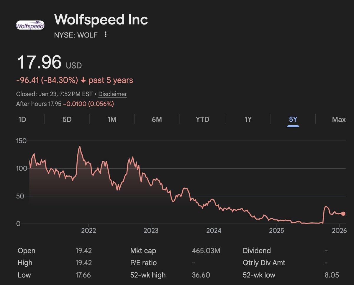
$WOLF ($464M) is the paradigm of the "Bear-Bull" Paradox.
Wolfspeed is the holy grail of AI with SiC wafers.
And this foundry just made the world’s first 300mm single-crystal SiC wafer last week.
$NVDA Rubin architectures likely need 300mm SiC interposers and Wolfspeed is the only company in the world currently that can do it.
They're critical to US national security with $750M in chips act grants.
I listed this as a bottleneck but here's the catch:
This is a negative EV trap:
- $926M cash, $2.1B debt, $465m MC
Ev would be roughly ~$1.6B.
Then you have
-> Convertible Notes #1
~$331.4 Million. Convertible into New Common Stock based on an implied equity value of $1.0 Billion.
-> Renesas Convertible Notes #2
~ $204 Million. (13.6% of the total shares)
December 15, 2025, Wolfspeed filed a prospectus to register 11.3 million shares for "selling stockholders"
These are the former creditors who took equity instead of cash during the bankruptcy.
So...
Wolfspeed is central to the SiC Interposer thesis for 2027 as they're made in America and are have a massive moat.
But this just looks like a trap right unless they can get this to massive scale and overshadow any convertibles, debt, and dilution.
This is on paper the holy grail of AI moonshots since they have the world's first 300mm SiC wafer and are a monopoly in as a US company.
But financially this is a landmine.
Disclosure: I own no positions, just wanted to post my findings.
18
15
231
82,180

6 Nov 2025
Avant IDE 2.0 :
• 14 jours pour analyser une conception
• Risques détectés tard dans le cycle
• Design manuel = erreurs coûteuses
Avec IDE 2.0 (IA intégrée) :
• 30 minutes d'analyse (vs 14 jours)
• Prédiction risques en 60 secondes
• Simulation multi-physique en cloud (thermique, électrique, contraintes mécaniques)
Le timing est parfait : explosion des Chiplets (plusieurs puces dans un boîtier) pour l'IA.
TSMC CoWoS saturé, clients cherchent alternatives rapides.
ASE propose maintenant "plateforme IDE 2.0 fabrication VIPack" = solution complète.
Résultat : plus de projets haute-valeur, clients captifs, marges en hausse.
TSMC fabrique les puces. ASE les assemble intelligemment.
3
311

21 Oct 2025
We’re thrilled to share that ASE today signed an #MOU with Analog Devices, Inc. (ADI) to acquire ADI’s manufacturing facility in #Penang, Malaysia — a major milestone as we strengthen our global footprint.
Malaysia continues to grow as a hub for advanced semiconductor manufacturing, and this partnership reflects our shared commitment to innovation and supply chain resilience. Following the acquisition, ASE and ADI plan to enter a long-term supply agreement and co-invest in expanding the Penang site’s technology and operational capabilities.
Our COO, Tien Wu, highlighted: “This strategic move broadens ASE’s global manufacturing capabilities and enhances our operational flexibility and scale.” Commenting further was ADI’s EVP of Global Operations & Technology, Vivek Jain, who underscored: “Together, we’re expanding Penang’s capabilities to strengthen our technology and support for customers.”
At a time when #semiconductor industry collaboration has never been more crucial, ASE and ADI are forging an even stronger presence in Malaysia — with a shared focus on innovation, upskilling, and growth.
For more: lnkd.in/gFakHEYn
#Semiconductors #Malaysia #manufacturing #innovation #collaboration #advancedpackaging #VIPack #AI
2
7
1,973

#News! Today we announced our collaboration with @aseglobal, the leading global provider of #semiconductor manufacturing services in assembly and test, to develop #3Dblox-based workflows for the ASE VIPack platform using our Innovator3D IC solution. 🔗 sie.ag/2cxUeb
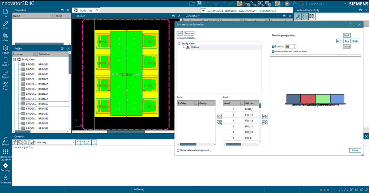
ALT Screenshot of Siemens Innovator3D IC software showing chip floorplan, component list, stack configuration, and 3D preview.
1
4
10
478

24 Sep 2025
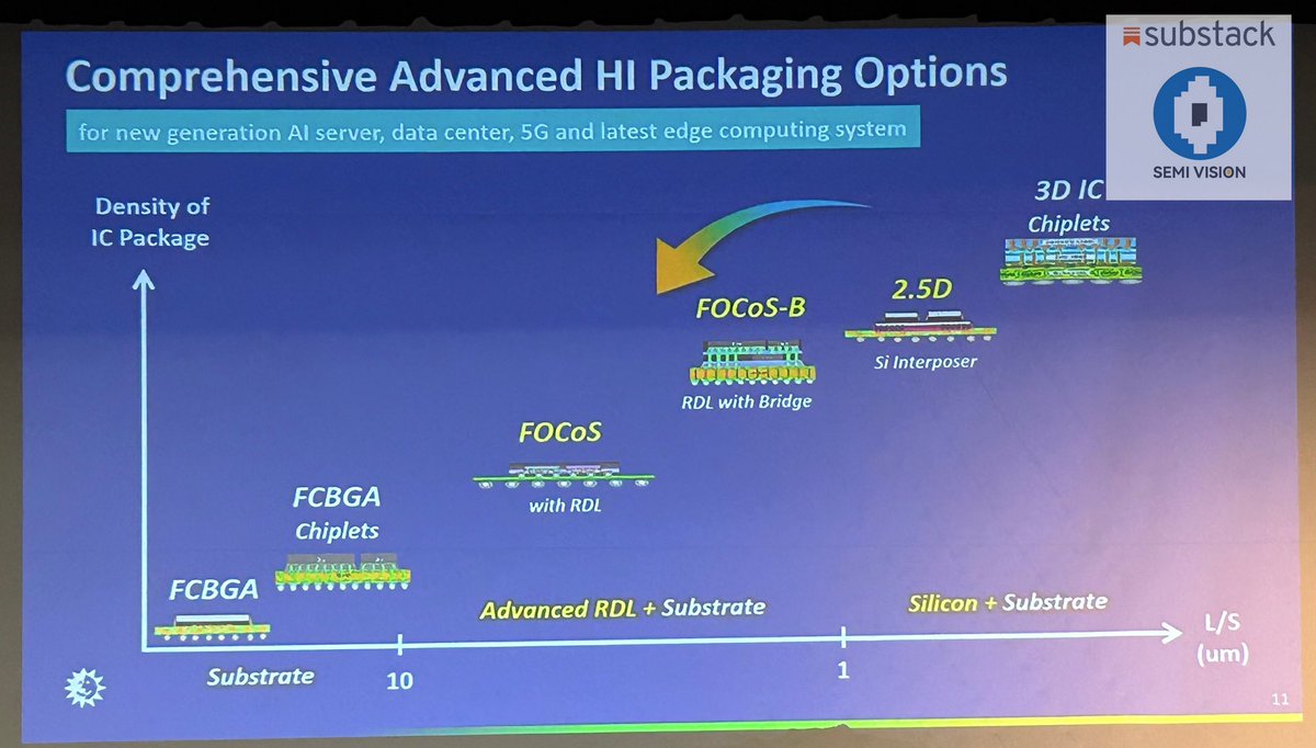
To address these challenges, foundries and OSAT (Outsourced Semiconductor Assembly and Test) providers are actively proposing solutions across different integration levels. For instance, Marvell has introduced the PIVR (Package-Integrated Voltage Regulator), embedding the VRM directly into the package to shorten the power path and reduce #PDN impedance, enabling faster voltage response. #ASE, through its VIPack and FOCoS-Bridge (with TSV) platforms, is optimizing PDN, signal interconnects, and thermal performance simultaneously—especially for Chiplet HBM packages that demand high bandwidth and I/O, enabling reduced power loss without compromising performance. tspasemiconductor.substack.c…

2
510
1 Jun 2025
ASE Semiconductor has announced the launch of its fan-out chip-on-substrate bridge technology with through-silicon vias (TSV), known as FOCoS-Bridge, to drive the advancement of artificial intelligence (AI) and accelerate its profound impact on global life.
The ASE FOCoS-Bridge leverages TSVs to enable shorter signal paths, achieving higher I/O density and improved thermal performance to meet the growing demand for bandwidth. The integration of TSV technology further enhances the capabilities of ASE’s VIPack FOCoS-Bridge platform, providing critical energy efficiency at a time when demand for AI and high-performance computing (HPC) applications is reaching unprecedented levels.
1
1
11
1,456
20 Mar 2025
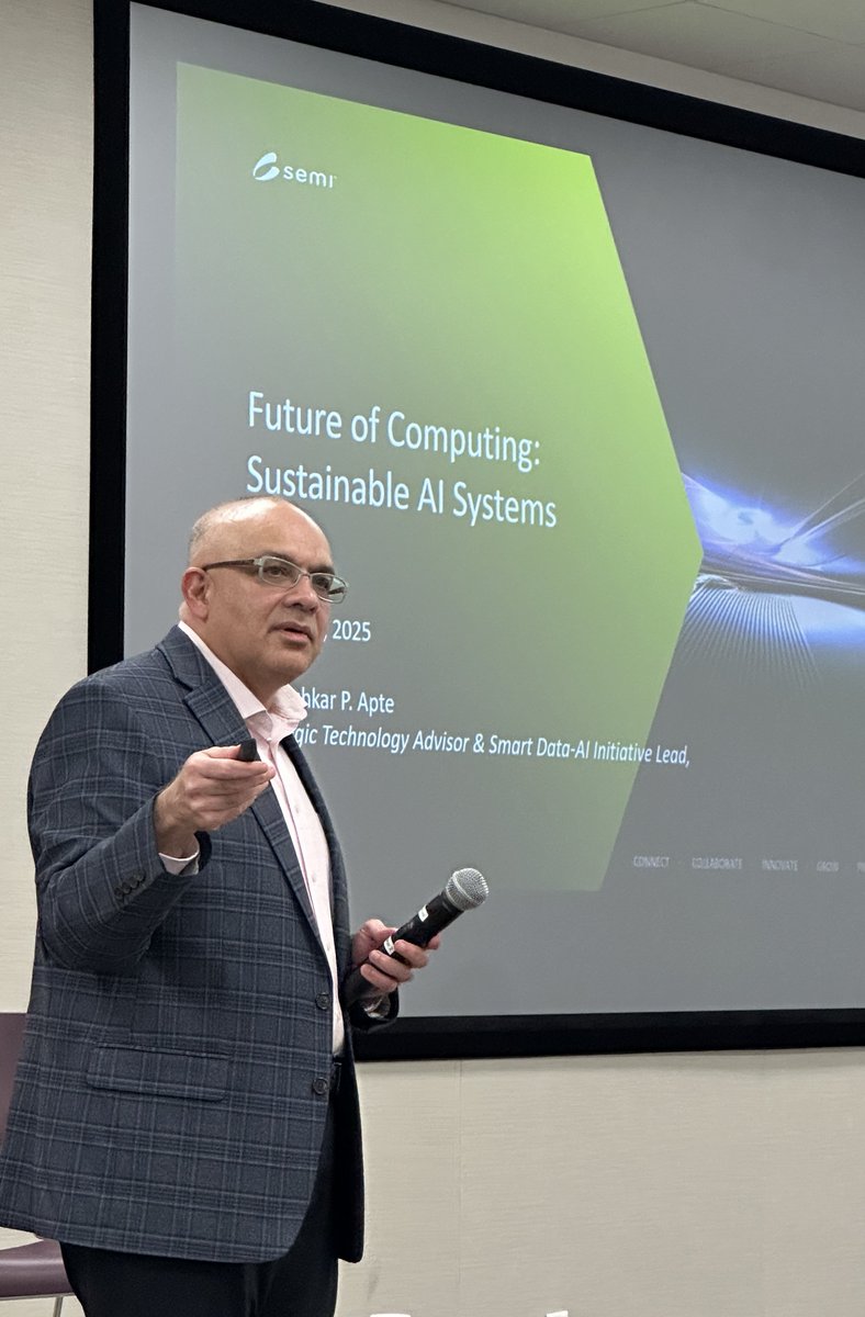
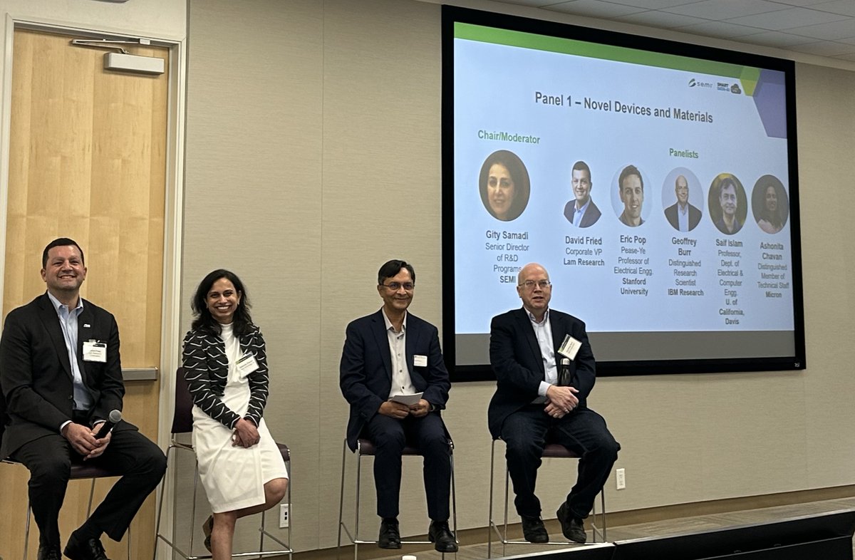
Agentic AI, robotics, and accelerated computing received top bill in the #SiliconValleythis week, between @nvidia 's #GTC25 and @SEMIconex's ‘Future of Computing’ workshop, which was indeed a triumph after being expertly put together by the indefatigable Pushkar Apte. Thank you to Ajit Manocha, Melissa Grupen Shemansky and Pushkar for setting the stage, elevating the SEMI value proposition, and facilitating this meeting of brilliant minds.
The premise of the workshop was Sustainable AI Systems, and speakers set forth the #AImodels and #datasets that are growing rapidly, giving rise to two fundamental challenges. First, this growth far outpaces performance improvement in hardware systems and infrastructure, and second, the energy consumption for AI continues to grow unsustainably. The challenges were thoroughly explored, examined, and explained. Perspectives were shared from opinion makers such as Jean-Philippe Fricker from @cerebras, Tristan Holtam from @Applied4Tech, John Hu from @nvidia, @profericpop from @Stanford, Chloe Jian Ma from @Arm, Wendy Zhu from @McKinsey, and many others. Yet, more questions than answers remain, signifying not only the crucial work ahead, but also the insatiable need for greater pathfinding and deeper collaboration across the ecosystem.
As the world’s leading #OSAT, it was highly encouraging to hear repeatedly throughout the workshop about the magic of #heterogeneousintegration, and the world of opportunities that #advancedpackaging technologies are opening up for the industry in our relentless quest for energy efficiency and power management to drive AI forward.
#CPO #materials #siliconphotonics #CPO #chiplets #photonics #datacenters #cloud #edge #agenticAI #robotics #acceleratedcomputing #VIpack #powerSiP #sustainability #energyefficiency #powermanagement


1
9
2,676
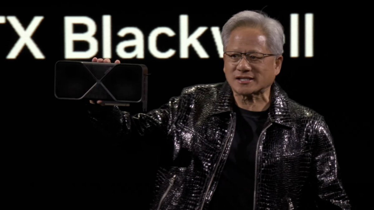
13 Jan 2025
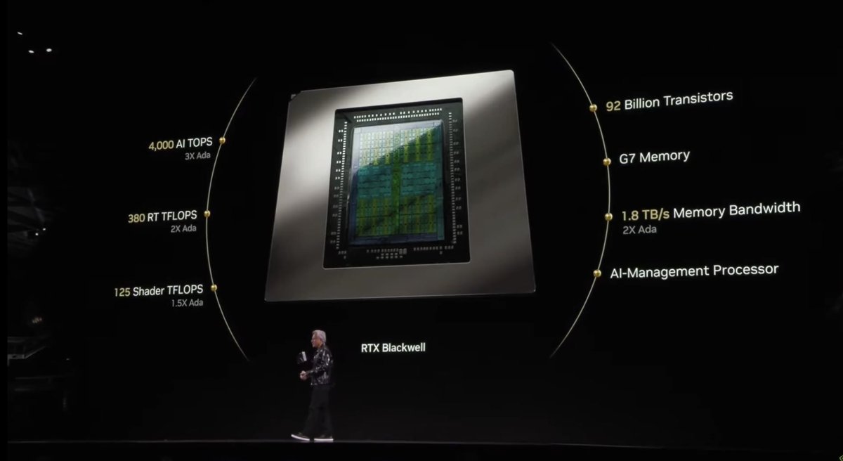
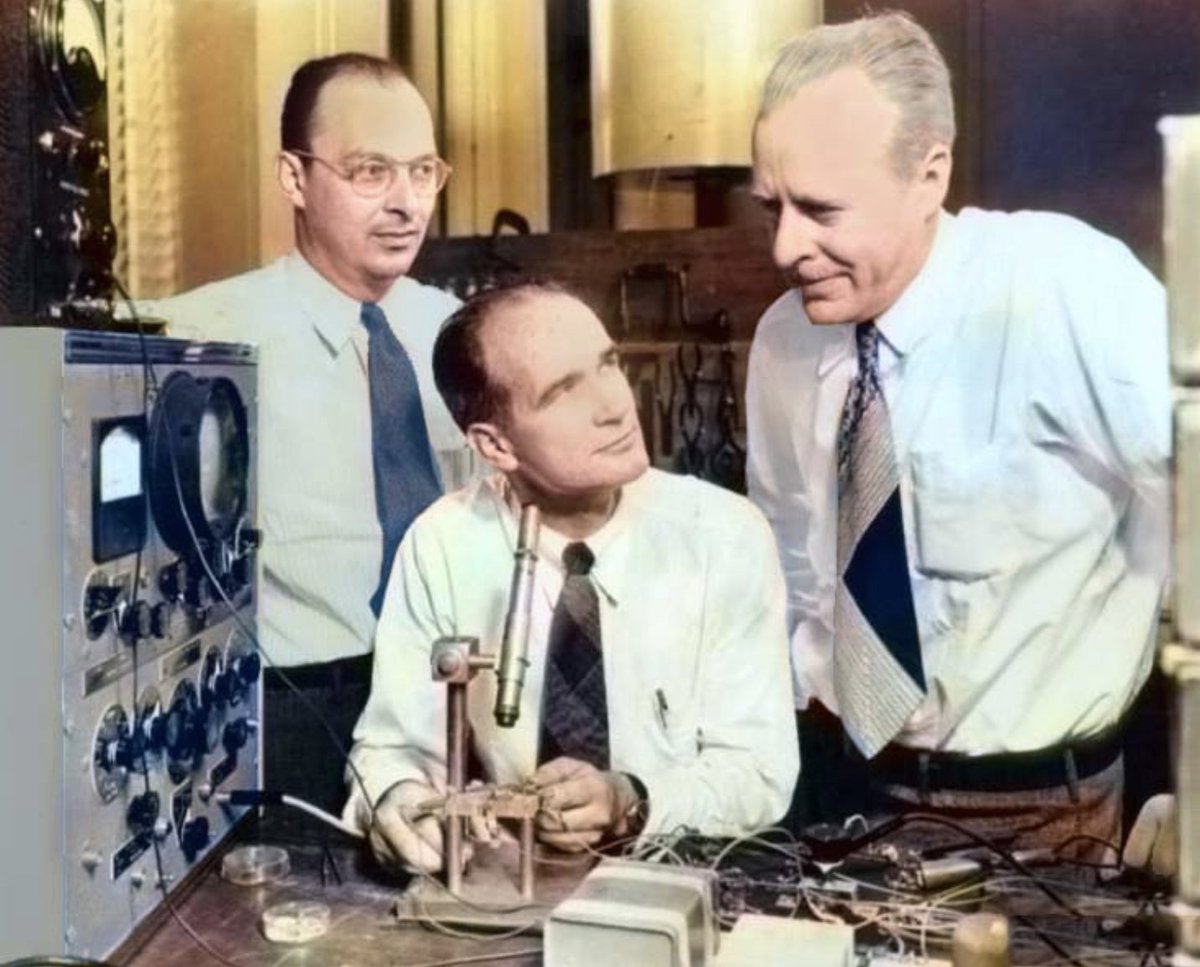
There was an electrifying atmosphere at the #CES2025 opening keynote delivered by @nvidia CEO Jensen Huang, who wore his huge engineering heart on the sleeve of his fancy #Vegas jacket, and announced some of their most advanced AI technologies to date. Powered by #Blackwell and #AI, he introduced new groundbreaking #GeForce RTX 50 series GPUs, designed for#gamers and #creators, to experience and deliver transformative and powerful AI experiences. Stunningly miniaturized, they are packed with power and performance, and fully loaded with #transistors, 92 billion transistors to be precise.
How incredulous Walter Brattain, John Bardeen, and William Shockley, would be! These three innovators invented the first transistor in 1947, but likely never conceived the generational impact of their invention. Today, transistors form the beating heart of all modern technology, and fuel what lies ahead for global society as the AI evolution continues. Robotics will play a huge role, with breakthroughs poised to emerge in many forms, including “agentic AI, humanoid robots, and self-driving cars,” according to Huang. Heterogeneous integration is truly at play, with #advancedpackaging bringing the magic. Here at ASE, it’s in our DNA.
#semiconductors #VIPack #Fanout #FOCoS #Bridge #Power #HPC #datacenter #robotics #agenticAI #humanoids #autonomous #selfdriving #4petaFLOPS #AIcompute #nobelprize #physics #siliconvalley @NVIDIAGeForce @NVIDIAAI #GPU
4
250
2 Oct 2024
Their conversation was intellectual and engaging, abstract and thought-provoking, meaning Jodi Shelton and Jensen Huang totally captivated the @GlobalSemi #USEF2024 audience. Industry executives drew from compelling anecdotes and deep wisdom gained only through overcoming challenges and experiencing triumphs over decades within the #semiconductorindustry. Jensen Huang recognized today's critical industry-wide technology quandaries where he underscored that at @nvidia it’s not just about the #chip, it’s about #systems, and these systems are “insanely complicated.” #Advancedpackaging is emerging as key, and as we move further into the #AI era, it feels like ecosystem collaboration has never been greater as collectively progress innovation and push boundaries further than ever imagined. #Datacenter #HPC #Power #Thermal #Scaling #VIPack #PowerSiP

1
6
521
27 Aug 2024
🎙️ Join us at #SEMICONTaiwan 2024 from September 3 – 6 at TaiNEX 1 & 2!
We’re gearing up for the industry’s greatest event of the season. This year, team @aseglobal will be taking the stage across various forum tracks, diving deep into industry insights, advanced #IC #packaging technologies, #AI innovations, #sustainability and #talent development.
👉 Swipe left for an exclusive preview of the week's exciting line-up!
#3DIC #CoWoS #VIPACK #Netzero #Engineeringtalent #STEM #DEI #AI #TechForGood


1
6
332
11 Jul 2024
ASE is excited to shared that our fully-owned subsidiary, ISE Labs, Inc. today announced that it is broadening customer access to its world-class capabilities with the opening of a second U.S. facility, located in San Jose, Calif. Together, the Fremont and San Jose sites will double ISE’s available R&D lab space, reinforcing the company’s commitment to Silicon Valley while expanding its North American footprint and helping to strengthen the U.S. semiconductor supply chain.
“We are firmly committed to our investment in Silicon Valley. It both contributes to the region’s revitalizing its position in the semiconductor industry and supports U.S. manufacturers more broadly. Adding this new high-end facility to our existing local footprint is an important step,” said Dr. Tien Wu, Chief Executive Officer, ASE, Inc. “Our ISE Labs division – the largest semiconductor testing service provider in North America – is essential to advancing ASE’s role in driving the development of the world’s most innovative electronics.”
ase.aseglobal.com/press-room…
#supplychain #SiliconValley #California #test #reliability #advancedpackaging #heterogeneousintegration #siliconphotonics #HPC #datacenter #VIPack

2
358
4 Jul 2024
Wishing everyone a wonderful July 4th holiday! On such milestone dates, we like to pay homage to all those across history who have blazed trails and spearheaded invention. Our industry is built on innovation and this July 4th, we pay tribute to all our employees, partners, and customers as we relentlessly working together to create a better future and sustainable world. #green #AI #VIPack #July4th #IndependenceDay #USA #Global #partnership
4
335
28 Jun 2024
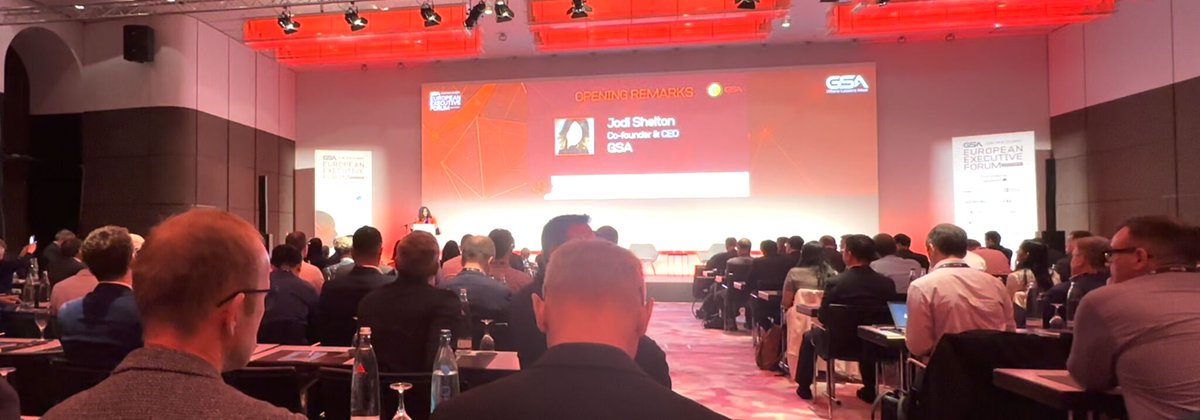
The Global Semiconductor Alliance European Executive Forum 2024 took place in #Munich last week - and ASE was there as a proud sponsor.
It was another meeting of brilliant #semiconductor minds expertly hosted by the inimitable Jodi Shelton, Sandro Grigolli, Kole Giles, Shungo Saito, and Caitlin Kelley, while featuring standout speakers, including Andreas Urschitz from @Infineon Technologies who delivered an impassioned presentation on our collective responsibilities as we journey further towards #decarbonization and #digitalization.
The agenda sparked much deliberation across an expansive range of topics, from #AI to #automotive, from #supplychain to #market, from #chiplets to #heterogenousintegration.
The need for semiconductor industry innovation has never been greater!
#sustainability #power #renewables #SiC #GaN #datacenter #HPC #generativeAI #sustainableAI #VIPack

6
281
28 Mar 2024
Team ASE were utterly enchanted by our gorgeous 3D-printed FOCoS-Bridge sample that garnered a lot of attention at the @IMAPS Device Packaging Conference last week in #Arizona. As such, it seems only right to share their enthusiasm here too.... #VIPack #FOCoS #Bridge #AI #HPC
Special thanks for supporting #DPC2024 to Mark Gerber, Lihong Cao, Sheng Li (李晟) , Thomas Smith, John Bosi, Elmer Gardiola, Steve Rosebaugh, Bill Stermer, Gil Caceres, Kelly R McKendrick Sr., Jie-Susan Cui, Steffen Priddy, Wiwy Wudjud, Danny Shen, and Roger Lo.
4
298

22 Mar 2024
ASE’s VIPack™ Enables Innovational AI Devices Through Advanced Interconnect Technology for Chiplets aseglobal.com/press-room/adv…
2
99