
Latham & Watkins Advised Ayar Labs In US$500 Million Series E Financing
Link to read full News: legaleraonline.com/global-de…
#LegalEra #DealNews #LathamWatkins #AyarLabs #SeriesE #Financing #ArtificialIntelligence #Semiconductor #CoPackagedOptics #Technology

18

Jun 12
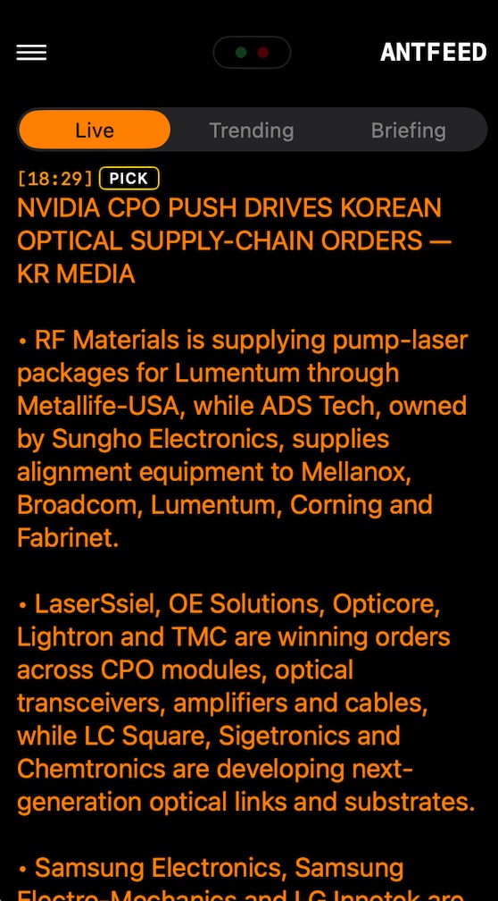
CPO GOLD RUSH: NVIDIA OPTICS BOOM LIFTS KOREAN SUPPLIERS INTO GLOBAL DEALS
TLDR: Nvidia’s CPO push is broadening the AI trade from GPUs and HBM into lasers, optical modules, alignment equipment, cables and silicon-photonics suppliers across Korea.
RF Materials, ADS Tech, LaserSsiel, OE Solutions, Opticore, Lightron, TMC, LC Square, Sigetronics and Chemtronics are gaining exposure to the global optical supply chain, while Samsung Electronics, Samsung Electro-Mechanics and LG Innotek expand CPO and silicon-photonics development as Nvidia, Broadcom and TSMC move next-generation networking toward mass production.
#Nvidia #CPO #CoPackagedOptics #SiliconPhotonics #OpticalModules #OpticalTransceivers #DataCenters #AIInfrastructure #Broadcom #TSMC #Lumentum #Corning #Fabrinet #Mellanox #Samsung #SamsungElectroMechanics #LGInnotek #KoreaSemis $NVDA $AVGO $TSM $LITE $GLW $FN $SSNLF $EWY $KORU $SMH $SOXX
2
2
35
3,493

Japan Photonics Series
[Part 5. Light Approaches the Chip, but Products Are Made in the Package]
Japan’s manufacturing leverage in the last few centimeters of CPO and optical chiplet packaging
Read previous:
Part 1: x.com/superposition_V/status…
Part 2: x.com/superposition_V/status…
Part 3: x.com/superposition_V/status…
Part 4: x.com/superposition_V/status…
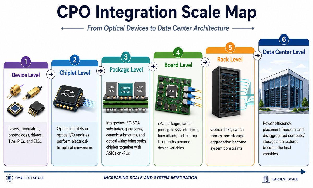
AI servers are defined by GPUs and HBM. But the real bottlenecks often appear one layer lower.
Chips generate more data, memory moves closer, networks get faster — yet all that data must still travel between chips, packages, boards, and racks.
CPO (Co-Packaged Optics) is one direct answer to this problem. It pulls the optical-electrical conversion point closer to the ASIC or xPU package, shortening the expensive electrical path.
1. Surface Signal: Optical I/O is moving from the board edge into the package
Traditional data-center optics placed the optical module at the front panel. Electrical signals traveled across the board to the transceiver, then converted to light.
CPO changes that. It brings the optical engine right next to the ASIC or inside the package, reducing electrical travel distance, power loss, and heat.
Shinko Electric describes its optical chiplet/CPO development as combining its semiconductor packaging substrate and IC assembly expertise with optical assembly and optical wiring technologies.
2. Hidden Mechanism: CPO must solve three interfaces at once
CPO is not just about putting light closer to the chip. It requires simultaneous optimization of three interfaces:
1) Electrical-optical boundary: driver, TIA, modulator, photodiode, laser (or external laser).
2) Chip-package boundary: optical chiplet, ASIC, interposer, substrate, thermal path, alignment.
3) Package-external boundary: fiber attach, connector, external laser routing, serviceability.
The governing variable is not bandwidth alone.
It is whether the entire link budget, heat, alignment, yield, test, and field serviceability can be solved together inside the package.
3. Japan’s companies operate across four functional layersJapanese players in the CPO/packaging layer are best understood in four layers:
Layer 1 — Optical engine & CPO assembly
Shinko Electric and AIO Core. Shinko brings optical assembly to its existing packaging substrate strength. AIO Core provides the compact optical transceiver (IOCore).
Layer 2 — Ceramic, thermal, hermetic reliability
Kyocera, NGK, NTK. These companies supply ceramic packages, submounts, and bonded wafers (e.g., InP/SiC) that manage heat, moisture, and long-term stability in harsh package environments.
Layer 3 — Substrate, interposer, optical-material patterning
Ibiden, TOPPAN, DNP, Resonac. They develop FC-BGA, glass-core substrates, organic RDL interposers, and panel-level processes that form the physical foundation for heterogeneous integration.
Layer 4 — System demand anchor
Kioxia shows how optical I/O can actually change system architecture (optical SSD, disaggregation).
#CPO #OpticalChiplet #CoPackagedOptics #Packaging #JapanTech #SiliconPhotonics #AIInfrastructure #DataCenter


Japan Photonics Series
[Part 2. Japan’s Optical I/O Targets 'Data-Movement Distance,' Not GPUs]
Read previous:
Part 1: x.com/superposition_V/status…
The realistic battlefield of storage–compute optical I/O shown by AIO Core, Kioxia, and KyoceraIf we treat the data center as one giant computer, bottlenecks do not only appear inside compute chips.
No matter how fast a GPU is, the processor waits if data does not arrive on time. The real problem of AI infrastructure is no longer just "how fast can we compute?"
It is increasingly "how far, how efficiently, and how reliably can we move data between memory, storage, and networks?"
#OpticalIO #StorageCompute #SiliconPhotonics #AIOCore #Kioxia #Kyocera #DataCenter #CPO #JapanTech #AIInfrastructure

4
13
77
11,639
[Part 5. 빛은 칩으로 다가오지만, 제품이 되는 곳은 패키지다]
CPO, Optical Chiplet, 패키징 계층에서 드러나는 일본의 ‘마지막 몇 센티미터’ 제조 레버리지
AI 서버를 보면 가장 먼저 GPU와 HBM이 눈에 들어온다. 그러나 실제 병목은 종종 더 낮은 층에서 생긴다.
칩은 더 많은 데이터를 만들고, 메모리는 더 가까워지지만, 그 모든 데이터는 결국 칩과 칩 사이, 패키지와 보드 사이를 지나야 한다.
1. 표면 신호: 광 I/O가 보드 가장자리에서 패키지 안쪽으로 이동한다
기존 데이터센터 광통신은 광 모듈을 보드 가장자리(프론트 패널)에 두는 구조였다. 전기 신호가 보드 위를 길게 이동한 뒤 광으로 바뀌었다.
CPO는 이 구조를 바꾼다. 광엔진을 ASIC이나 xPU 패키지 가까이로 가져와 전기 신호의 이동 거리를 줄인다.
Shinko Electric은 optical chiplet/CPO를 개발 중이며, 기존 반도체 패키징 기판과 IC assembly 기술에 optical assembly와 optical wiring을 결합하고 있다고 설명한다.
2. 숨은 메커니즘: CPO는 세 개의 접면을 동시에 다룬다
CPO의 본질은 단순히 빛을 칩 가까이 넣는 것이 아니다.
세 개의 접면을 동시에 풀어야 한다.
1) 전자-광자 접면: driver, TIA, modulator, photodiode, laser
2) 칩-패키지 접면: optical chiplet, ASIC, interposer, substrate, 열 경로, 정렬
3) 패키지-외부 접면: 광섬유, 커넥터, external laser, 서비스성
지배 변수는 대역폭 숫자가 아니라, link budget, 열, 정렬, 수율, 테스트, 서비스성을 동시에 만족시키는 능력이다.
3. 일본 기업들은 네 개의 기능 계층으로 보는 것이 정확하다
CPO·패키징 계층에서 일본 기업들은 한 묶음으로 보면 오히려 흐려진다. 각 기업이 맡은 위치가 다르기 때문이다.
1계층: optical engine & CPO assembly
Shinko Electric, AIO Core
2계층: ceramic, thermal, hermetic reliability
Kyocera, NGK, NTK
3계층: substrate, interposer, optical-material patterning
Ibiden, TOPPAN, DNP, Resonac
4계층: system demand anchor
Kioxia (optical SSD, disaggregation 수요)
#CPO #OpticalChiplet #CoPackagedOptics #Packaging #JapanTech #SiliconPhotonics #AIInfrastructure #DataCenter
1
8
39
2,354

May 23
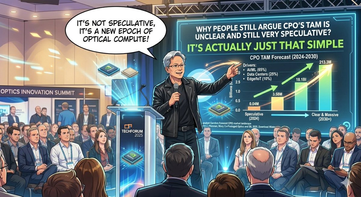
Why Are some FinX accounts Still Saying CPO TAM Is ‘Unestimable & Speculative’?
CPO TAM has a structurally defined ceiling
= total DC connectivity chip demand
(fixed by physics: every GPU cluster needs optical interconnect)
GS anchor: optical networking TAM 9x → $154B by 2028,
CPO alone = $91B at just 29% scale-out penetration
TSMC macro: global semi >$1.5T by 2030,
AI/HPC = $825B (55%) — larger than today's entire chip market
CPO captures a growing slice of that $825B
as optics content per GPU is 5-10x higher vs. pluggables
→ CPO addressable range: $200B–$500B at full penetration
Only variable = adoption speed:
Fast (2030 full migration) → CAGR ~130%
Slow (2035 full migration) → CAGR ~70%
Either way: the ceiling is enormous.
The only bet here is timing, not existence.
$COHR $LITE $AAOI $SIVE
#CPO #CoPackagedOptics #AIInfrastructure
3
27
2,818

May 18
今天大家都在发表对于Leopold Aschenbrenner 刚刚提交的他2026年Q1的13F持仓报告。
他清仓了 $LITE和 $cohr卖出了全部,并且一股不留。大多数人都认为这代表着Leopold 看空光子学,并且认为光子学泡沫太高。
同时他也买入了大量 AVGO、TSM 和 $SMH 的看跌期权。这被视为一种保护策略的同时也是一种看跌情绪的表现。
但我认为完全不同,我们需要理清楚逻辑:
1. 这个F13 披露的是季末持仓,滞后45天。所以说你看到的是过去,不是现在。
Q1是1月1日 到3月31日,然后最后的截止提交日是5月15日。
2. 所以说我们往前推算45天能获得什么? 我直接按照4月1号的价格来大约估算一下 光学行业里 $lite 上涨了20%, $cohr上涨了 40%左右,我们买入的第一持仓 $sive 上涨了500%。
3. 他离场的同时,光学还在上涨,他的离开不代表着光学的消失和终结。如果我们今天散户用滞后数据构建叙事,本质上是在追踪一个幽灵,所以会造成散户的大量抛售。
4. 市场的抛售是源自于散户的恐慌,而我们如果深度学习光学行业,那你会发现CPO供应链尚未被发现,还没开始大规模量产。
如果他的这份报告里什么是值得重视的则只有看跌期权。
因为这本身是一种对冲一个他认为真实存在的下行风险,而不仅仅是获利了结后的仓位优化。宏观层面的担忧可能比叙事上描述的更深。
所以存储方面,我们才是更需要关注的。
我认为你现在看到的消息是机构想你看到的,至于Leopold 现在的真实持仓,可能和这份文件完全不同。他或许都已经在今天的下跌中可能已经重新建仓 $LITE,所以看光学基本面,一切没改变的话,这会是一次很好的加仓机会。
#SIVEF #LPKF #CPO #CoPackagedOptics #13F #Semiconductors #PreDiscovery #AIInfrastructure


1
16
13,705
May 16
韩国人开始入场 $sive, 这意味着 $sive正进入另外一个阶段。这家公司正吸引着全球最庞大,最有赌性,且最高度活跃的散户群体的关注。
为什么韩国市场如此重要:
首先,韩国是一个全民炒股的国家,他们的账户数超过人口总数,这意味着他们人均拥有俩个股票账户。这能给 $sive带来巨大的增量
其次韩国投资者的特点决定了他们一旦认定一只半导体小盘股符合”AI赛道+技术壁垒+即将双重上市”的叙事,极有可能形成群体涌入效应:而 $sive 符合所有条件, 他们有光学 无线技术,同时他们也准备在纳斯达克上市。
如果韩国投资者加入,他们偏好高杠杆短线操作,其股价可能会剧烈波动,这意味着会有很多买入和卖出的机会。
而散户的大量购买会引发分析师覆盖和机构兴趣,这对 SIVE 在纳斯达克双重上市的定价有正面意义。
可能说这些话会让大家觉得宽泛,那我举出几个韩国人在股市方面创造的奇迹:
1. 在经历了2019冠状病毒病疫情之后,大量韩国散户开设股票账户,在疫情初期韩国股票暴跌,大量韩国散户购入韩国股票,让股市稳定下来,事后散户的行为被称为”东学蚂蚁运动”。 这是一次韩国散户托举起韩国市场的典型案例。
2. 有韩国人真实的在 SK海力士里赚取了400倍收益的叙事,往往真实的故事更能凝聚大家的自信心。
3. 韩国散户在早期大量建仓买入 $kioxia,而该公司在登陆东证所后股价已飙升24倍。
我说的是大多数的散户,我也相信有其他国家的人也能超过几十倍的收益,但韩国散户是大多数获得高收益的群体。韩国散户的金融敏锐度是真实存在的——他们对半导体产业链的理解深度、全球扫货速度、以及在关键节点逆势入场的胆量,都远超一般认知。
#SiversSemiconductors #SIVE #SIVEF #CoPackagedOptics #CPO #PhotonicsSemiconductors #AIInfrastructure #OpticalIO #InPhLaser #NasdaqListing #AIDataCenter #5GmmWave #SmallCapTech #SemiconductorInvesting #AyarLabs
May 16

$sive
스웨덴 주식 매수방법을
궁금해 하시는 분들이 많아서 답변 드리겠습니다
특정 증권사와 관계없고
질의가 계속 와서 정보공유차 공유합니다
저도 요즘 세상에 주식 전화주문한 건 신기한 경험입니다.
1. 증권사 해외주식 상담파트(저는 kb)에 전화를 한다
2. 해외주식 매수를 하려고 한다고 말하고, 정확한 주식명을 말한다
3. 안내사항을 직원분이 말해준다.
-스웨덴 장은 오후 4시 개장이고, 4시 이전에는 환전만 가능
-오후 4시 이후에 환전과 주문이 둘다 가능함
-중개수수료가 기본 5만원 정도의 수수료가 있음(300sek로 기억)
-중개 수수료가 기본 5만원 정도vs 0.5% 둘 중에 싼 것을 적용
예를 들어 100만원어치 주문해도 5만원(기본)
1000만원어치를 주문해도 0.5%인 5만원
-매수 가격을 지정해서 말해주어야함
-매수체결이 되어도 전산개발이 덜되어, 보이기는 하나 클릭하면
이상하게 보임(kb증권 기준)
-원화 환전을 스웨덴 크로나로 함
-일본 주식처럼 100주단위 이런건 없음. 수수료가 비쌈
-매수체결이 안되면 그 다음날 또 전화해서 매수체결 해야함
더 궁금하신 부분 있으시면 아는 선 내에서 답변 드리겠습니다.
19
28
205
55,205
May 15
所以现在的情况是 $AMZN与AlChip有一个新的私募。
然后AlChip是Ayar的潜在客户。而 $SIVE是Ayar的主要激光供应商。
那么这样看起来 $sive在未来可能会和亚马逊有合作的可能性?
那现在的大型机构的潜在合作看来包括但不限于:(只是可能性,猜测)
1. $NOK 和 $sive的合作关系可能是 $sive进入英伟达生态有潜在推动。
2. 市场上未经验证的预测,Sivers 的激光设计专长与苹果在健康应用光学传感方面的野心联系到一起,新一代的手表?为什么会这样想因为Sivers Photonics 的 DFB 激光芯片专为消费级传感应用提供紧凑、稳定、高效的光源,覆盖生物特征识别、健康监测到环境检测——正好对应智能穿戴、AR/VR、健康监测仪器等下游场景。
3. AlChip是Ayar的潜在客户这一条线,让 $sive可能进入amazon生态。
4. CPO/ELS 方案的终端买家是 Meta、Google、Microsoft、Amazon 等超大规模云厂商——Sivers 处于供应链上游。
我觉得可能性大的会是 $nvda 和苹果,亚马逊。
另外对于 sive这样的激光阵列核心供应商,它不需要直接拿下七巨头订单,而是通过 Ayar Labs、Aeva、POET、O-Net 等中间层间接进入七巨头的数据中心和自动驾驶生态。
#SIVE #SiversSemiconductors #Photonics #CPO #CoPackagedOptics #AIDataCenter #LaserArrays #AyarLabs #Nvidia #Apple #Mag7 #Semiconductors #OpticalIO #AIInfrastructure #SmallCapStocks #TechInvesting #LiDAR
May 15

Just to add to the very positive $SIVE news amid MSCI likely tens of millions of inflow in 2 weeks:
$AMZN has a new private placement with AlChip.
Probably implying design wins with future Trainium.
If you don’t remember… AlChip was Ayar’s lead customer. And $SIVE is the primary laser supplier to Ayar.
So implications for $SIVE, is enormous piggybacking off of Amazon’s ecosystem growth.


4
5
24
8,153

所有人都在买GPU和存储。没有人告诉你光模块公司的总市值比美光还低
我想从一个反常识的问题开始:GPU是AI的大脑,存储是AI的记忆。那光是什么?光是AI的神经系统。但神经系统从来不是最先被注意到的。存储已经涨了10倍,GPU更不用说。光的时代,刚刚开始。
1. 先说一个结构性的错误定价
在Nvidia的NVL72机架里,光模块的采购金额占到整个机架的20%。2026年全球AI光收发器市场规模预计从2025年的$165亿增长到$260亿,同比增速超过57%——这是半导体赛道里增速最快的子领域之一。 但所有光模块公司的总市值,比美光一家还低。这个错误会被纠正。问题只是什么时候。
2. 光和存储不一样的地方
存储的接力是季度级别的事件——供需拐点,财报超预期,市场重新定价,SNDK从$200涨到$900,这个过程很快。光的接力是年级别的结构性变迁,因为光的技术路线本身正在发生一次范式转移:
第一阶段(现在):可插拔光模块
800G → 1.6T → 3.2T
线性增长,随数据中心扩张
第二阶段(2026下半年):近封装光学NPO
光模块移向芯片旁边
需求非线性跳升
第三阶段(2027-2028):共封装光学CPO
光引擎直接封装进芯片
这是终局,也是最大的价值重构
Meta在OFC 2026分享了大量数据,证明CPO比可插拔光收发器更可靠,成本更低,功耗更少。Nvidia在GTC展示了CPO将在2027/28年用于Scale-Up互连。5年内所有AI数据中心互连都将是光。 这不是预测,是物理定律。铜在高速率下信号损耗太大,功耗太高,距离太短。光没有这些问题。
3. 光在吃铜,不只是光吃光
生成式AI集群需要比传统云服务多10到100倍的光纤,正在把现有铜互连逼到物理极限。 这是大多数人没想到的逻辑——光的增长不只来自数据中心规模的扩大,还来自光替代铜的渗透率提升。每一代迭代,光吃掉更多铜的市场。这是双重驱动,不是单一驱动。
4. 产业链七个卡位,从上游到下游
现在我来把整条产业链拆清楚。
七个公司,覆盖从最上游的衬底到最下游的网络设备。
🔬 最上游:硅光衬底 $SOI
做的是硅光PIC的衬底材料——整个产业链最上游的原材料。没有SOI的衬底,硅光芯片就没有基础。护城河极高,几乎没有竞争对手能短期内介入。和TSEM形成上下游绑定:SOI提供衬底,TSEM代工成芯片。
🏭 代工层:硅光晶圆厂 $TSEM(Tower Semiconductor)硅光版本的台积电。
今天刚刚发生的重大事件:
TSEM宣布签署$13亿的2027年硅光合同,收到$2.9亿产能预付款,2028年还有更大合同在谈判中。计划资本支出$9.2亿专门用于硅光扩产,Q2营收指引$4.55亿同比增22%。
TSEM最聪明的地方在于:它不赌哪条技术路线赢。
可插拔、NPO、CPO,三条路线都用TSEM代工。就算市场对技术路线判断错了,TSEM依然受益。这是光通讯产业链里确定性最高的picks-and-shovels。
💡 激光器层:光的心脏
光模块的核心是激光器。没有激光器,光模块什么都不是。
激光器分两条技术路线:
磷化铟(InP)路线——$LITE(Lumentum)
LITE是目前唯一能量产200G每lane EML激光器的供应商,是1.6T收发器的关键零件。Nvidia预先锁定了LITE的EML产能,推迟交货期超过2027年。
Nvidia向LITE投资$20亿,用于加速AI基础设施光学技术。LITE CEO称2026年是激光器芯片销售的"突破年",刚收到历史上最大的CPO超高功率激光器采购承诺。
LITE的护城河是时间积累的——InP激光器的制造需要极其精密的工艺,20年积累的经验是任何竞争对手短期无法复制的。而且LITE不只押注现在:EML是可插拔时代的命门,ELS外置激光器是CPO时代的命门,OCS光路交换机是未来AI集群的光学路由器。
三个产品线覆盖了光通讯从现在到2030年的完整需求。
硅光(SiPho)激光器路线——$SIVE(Sivers Semiconductors)
Sivers专注于CPO系统的高性能InP激光阵列,Jabil合作是第一个商业验证信号,证明技术正在从研究走向真实超大规模部署。 SIVE不是要打败LITE,而是作为CPO时代激光器供应链里的补充供应商——当LITE和COHR产能不足时,SIVE是下一个选项。整个CPO产业的激光器供应严重短缺,补充供应商的价值会被重新定价。
🔭 光学系统层:从组件到整合
$COHR(Coherent Corp)
COHR最新Q3财报:营收$18.1亿同比增21%,数据中心和通信板块$14亿,同比增40%。Nvidia同样投资$20亿入股COHR。COHR是整个光通讯赛道里垂直整合程度最高的公司。从InP晶圆到激光器到光模块到系统,全部自己做。COHR正在扩大6英寸InP晶圆产能,这是推动毛利率持续提升的核心驱动力——规模越大,每片晶圆的成本越低,利润越高。
LITE和COHR的关系是竞争者也是互补者:
LITE:激光器专家,EML垄断,聚焦
COHR:光学系统整合商,体量更大,更全面
🏗️ 物理基础设施层:光纤和连接 $GLW(Corning)
Corning是光通讯产业链里最让人意外的标的——一家成立于1851年的玻璃公司,正在成为AI基础设施的核心受益者。
Q1 2026光学通信业务增长36%,分部净利润增长93%。2028年营收目标$300亿,2030年$400亿,内含年化增速19%。两个额外的超大规模云厂商签署了长期协议。
Nvidia命名Corning为下一代AI基础设施光连接合作伙伴,投资$5亿 最高$32亿股权,在美国建三座专属光学工厂。
Corning做的是光纤、线缆和连接器——不是最性感的产品,但是不可或缺的基础设施。
城市要运转,不只需要主干道,还需要所有的小路、接头、路牌。
Corning做的就是光通讯世界里的所有"小路和接头"。
而且这些"小路和接头"是消耗品——每建一个数据中心都需要,每升级一个机架都需要。
📡 网络层:AI时代的网络基础设施 $NOK(Nokia)
Nokia是这七个标的里最被市场误解的。大多数人还在用"翻盖手机公司"的眼光看Nokia。
Nokia 2026营收预期同比增长7.5%,EPS增长21.2%,光网络业务增速20%,AI和云业务增速49%,单季度新增€10亿AI和云订单。
Nokia做的是什么?
光传输网络(OTN)——把数据中心之间用光连接起来的骨干网络。这是Scale-Across的核心基础设施。
Nokia的第六代超相干光学技术PSE-6s,是目前全球少数能实现800G甚至1.2T长距离光传输的技术之一。
Nokia收购Infinera之后,从"转卖别人芯片的公司"升级为"拥有自己光芯片工厂的公司"——同样的技术路线,市场给LITE估值66.5倍,给COHR估值35倍,Nokia只有30.8倍Forward PE。
这个估值差距是最大的错误定价之一。
七个标的的完整产业链图
最上游
SOI(硅光衬底)
↓
TSEM(硅光代工)
↓
激光器层
LITE(InP EML,可插拔 CPO)
COHR(垂直整合,光学系统)
SIVE(CPO激光阵列,高赔率)
↓
物理基础设施
GLW(光纤、线缆、连接器)
↓
网络层
NOK(光传输网络,骨干连接)
每一层都有自己不可替代的护城河。
每一层都在受益于同一个趋势。
6. 为什么是现在?
2026到2027年是在1.6T供应链建立立足点的关键时期,在一线客户的设计导入将决定长期赢家。现在是design-in阶段——产品正在被超大规模客户选中和锁定。等量产阶段到来,市场才会充分定价这些公司的价值。
在design-in阶段买入,等量产阶段收获——这是光通讯投资最好的时机。
7. 仓位逻辑
高确定性(重仓):
TSEM → 今天$13亿合同,产业链里最硬的催化剂
LITE → EML垄断 Nvidia锁定,现在到2028年都受益
COHR → 垂直整合,体量最大,Nvidia $20亿入股
中等确定性(配置):
GLW → Nvidia直接合作,物理基建不可或缺
NOK → 最被低估的估值,但故事兑现需要更多时间
高赔率(小仓位):
SOI → 和TSEM绑定,护城河高但流动性低
SIVE → CPO时代的纯粹赌注
8. 光会接力存储吗?
会。但不一样的方式。存储的接力是一次性的价格重估——供需拐点到来,几个季度内完成定价。
光的接力是分阶段的持续重估——
2026年:可插拔1.6T带来第一波
2027年:CPO开始量产带来第二波
2028年:Scale-Up全面光化带来第三波
三波叠加,才是光通讯超级周期的全貌。存储让你在一年内赚了10倍。光可能让你在三年内赚同样多,但过程更平稳,确定性更高。
最后一句话
光通讯不是一个新故事,是一个被重新发现的旧故事。
光纤已经存在几十年了,但AI让这个故事的量级发生了质变。每当数据中心需要更高密度、更低功耗、更远距离的连接时,答案永远是光。
#光通讯 #TSEM #LITE #COHR #GLW #NOK #SOI #SIVE #CPO #硅光 #光模块 #AI基建 #数据中心 #存储接力 #Nvidia #美股 #USStocks #SiliconPhotonics #CoPackagedOptics #EML #光互连 #AIInfrastructure #光纤 #Nokia #Corning #Coherent #Lumentum
91
618
2,110
637,008
May 14
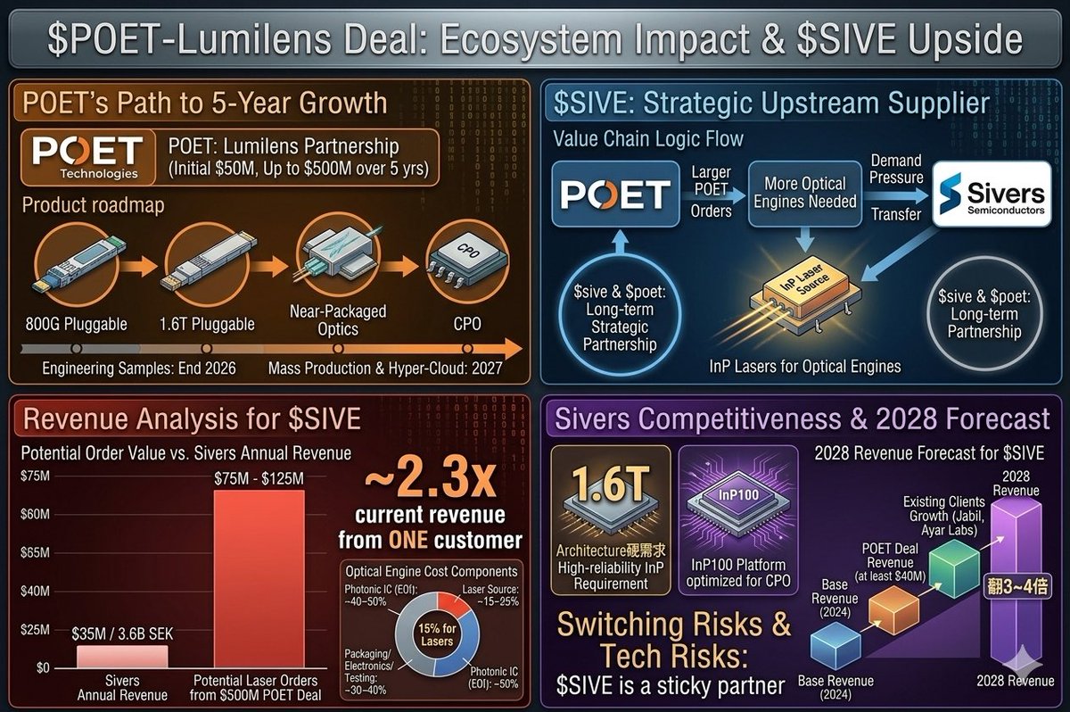
今天 $POET 的订单让他们一度涨超30%, POET Technologies 今日宣布与 Lumilens 达成合作,初始采购订单 5000 万美元,五年累计可达 5 亿美元 。产品路线图覆盖 800G、1.6T 可插拔收发器,再到近封装光学和 CPO,工程样品预计 2026 年底,量产对接超大规模云厂商在 2027 年。 这一次合作能覆盖 $poet的所有上下游,具体内容如下:
1. $sive 会收到间接的利好影响,因为 $sive和 $poet 有着非常好的长期合作关系,其核心POET 是 Sivers 激光器的买家。所以,POET 拿到更大订单 → 需要更多光学引擎 → 理论上需要更多 Sivers 的 InP 激光器作为光源。这条逻辑链是通的。 所以作为上游的激光器供应商,订单压力会传导给 $sive。
2. 我们可以做一个模型,比如激光器成本占模块成本的15%,5亿美元订单对应的激光器采购额粗估在7500万~1.25亿美元之间。对比Sivers目前全年营收才3.6亿瑞典克朗(约3500万美元),这一个客户的潜在订单就可能相当于其现有营收的**23倍。
为什么我这样算?
在一个光学引擎模块的成本构成大致是:
1. 光子集成芯片(POET的EOI):约40~50%
2. 激光器/光源:约15~25%
3. 封装、电子元件、测试:约30~40%
所以我算的15%是很合理的。
3. 我们看 $poet 的整体路线图:800G → 1.6T插拔式 → 近封装光学 → CPO。 其中sivers的核心竞争力是在1.6T架构下故障率上升,InP方案成为硬需求。 这是刚需不容易改变。
4. $sive作为核心合作伙伴,POET切换供应商有技术风险和认证成本。并且,Sivers的InP100平台专门针对CPO场景优化,适配性强。
所以我认为, $poet的这一份合同会直接利好公司本身,但其带来的大量订单会让 $sive收益。如果这一份订单确认,那么 $sive从这一个订单上就会获得至少4千万美金的营收在2028年。如果再加上Jabil、Ayar Labs等现有客户的同步增长,2028年营收翻3~4倍在数字上是站得住脚的。
非常看好! 可能这是我个人的揣测 不一定真实,但他们确实有合作关系,他们也确实存在上下游关系。
唯一的风险则是5亿美元是上限承诺而非保证,实际履约取决于Lumilens自己拿到多少超大客户订单。
但不论怎么说 ! bullish! YOLO!
$SIVE $SIVEF $POET $JBL $NVDA $LITE #CPO #CoPackagedOptics #OpticalIO #InP #Photonics #DFBlaser #1point6T #ELS #AIInfrastructure #AIDataCenter #OpticalNetworking #GPUInterconnect #Semiconductor #SmallCap #HypergrowthStock
3
1
12
2,320
May 13
我想和大家分享一下我所持有的台湾股票,我对他们的期望是在今年有2x的表现,他们分别是:
1. 上诠: FOCI (3363)
这家公司属于CPO概念股,是台湾光纤通信元件制造商,2026年Q1财报表现不佳,每股亏损 0.98 元,4 月营收年减 37.3%, 主要因传统业务下滑、同时大量投资新产能所致。但他们的资本支出却扩大数倍,其中超过2/3的资金投入到CPO FAU 自动化生产与测试机台。从这点我感觉他们是在为之后的量产做准备。
他们产能的变化也和他们的财报相符合,2026年是上诠进入CPO量化元年,其生产线扩大,并且他们的LPO(线性驱动可插拔光学)产品在2026年开始贡献营收,这是积极的一部分。 同时1.6T 产品也会在Q3季度贡献营收。
他最主要的客户则是 $TSM ,而潜在客户也有很多:
1. 他们深度参与了和台积电的COUPE 平台矽光子供应链。
2. 下有潜在客户包括但不限于 $nvda, $amd,marvell, cisco 等芯片大厂。
3. 云端大厂开始规划纵向扩展型 CPO 战略,并向供应商作出承诺。
4. 微软也会是他们的最终潜在客户。
3363 这家公司并不缺少想象力,因为他们的核心客户就是 $tsm, 而台积电的终端都是超级大型公司。
第二家公司我买入的是 讯芯 KY (6451)
作为一家从传统组装厂转型为尖端技术领航者,并且有着全球领先的系统模组(SiP)与高速光纤收发模组封装测试服务提供商,我对他的期望很高,我认为当前股价只反映了他实际市值的70%。
首先,我非常喜欢他新任ceo的背景:
1. 前台积电共同营运长
2. 同时担任鸿海集团半导体策略长
另外,6451的技术核心分三个,
其一是高速光纤收发模组封装用于发展1.6T。
其二是系统单封装,他能把多个不同功能的芯片整合到一个封装,这样的技术带来的利益是产品更小、更省电,耗能更少。另外因为地缘政治的缘故,美国 IDM 客户要求产能转移至东南亚,所以该技术订单扩张迅速,我非常看好这一点。
其三则是CPO模组封装,这是他们比较好的护城河,因为在这条赛道上他们已经和客户有着5年的合作时间,所以有着先发优势。并且同时该技术难度系数极大,可替代性极小,Edge coupling(边缘耦合)比常见的光栅耦合(Grating coupling)损耗更低、效率更高,但工艺难度也更大。
财报方面和FOCI类似都是不及预期,其主要原因是新产能尚未完全开出。我认为这是因为衔接问题。 或许是该行业的通病——产能受限。
最后一家公司则是汎铨 (6830)
他的定位比较特殊,因为是一家半导体检测分析服务商。 那他有什么潜力能上涨数倍呢?
首先,他们的主要业务——材料分析的市场占有率在台湾可以达到60%以上,他们甚至可以给2奈米甚至是1.5纳米级别的工艺做结构解析。
第二个技术则是矽光子检测,这个的市场占有率达到90%以上。
所以他的潜力就在于他所在的行业内他是垄断地位,并且还未被定价。他们在美国,台湾,日本都有专利。
目前为止,我没看到几家在半导体企业里有垄断技术的公司。
如果CPO 大规模商用,每一片矽光子芯片都要过汎铨这一关,营收天花板将大幅提。 而CPO的进程我估计是在27年初到28年中这个时间段,为什么? 高盛认为光学投资在未来俩年能达到1500亿,CPO就占910亿。
另外,该公司也在兜售设备,设备单台最高6千万元………然后他们还有售后服务,那更加绑定客户粘性。并且汎铨在竹北厂区为美国 AI 芯片大厂(如 NVIDIA)设立专区,采「包场低消」形式确保基本营收底线,且专区空间预计在 2026 年中从 25% 扩增至 75%。
这三家公司在CPO领域里分别是:上诠负责光纤进入矽光芯片的”入口”,讯芯-KY 负责整个 CPO 模组的最终封装与测试,而汎铨则是“医生”。
#CPO #矽光子 #SiliconPhotonics #AI数据中心 #AIDataCenter #先进制程 #埃米世代#FAU #CoPackagedOptics #800G #1point6T #COUPE #台积电 #TSMC #汎銓 #6830 #上詮 #3363 #訊芯KY #6451

8
11
110
9,373
May 7
今天的剧情还是太熟悉了,瑞典从早上就开始砸盘到下跌10%,现在接近美股开盘 $sive 只下跌了2%。 看来他们也清楚地知道不论他们卖的有多严重,美国人都会买起来。
为了新粉丝们知道 $sive 这一家公司有多大的潜力,我和各位简单的总结一下:
首先公司在光子和无线领域有着接近60年的研究,然后公司通过两大业务板块运营——无线(Wireless)和光子(Photonics),开发、制造并销售芯片、组件、模块和子系统,面向北美、欧洲和亚洲市场。
🤝 已确认合作(现有)
📡 光子 / AI 数据中心方向
Ayar Labs(美国):
Sivers 的激光阵列集成于 Ayar Labs 的 SuperNova™ 多波长光源,支持 4 Tbps 数据通信。 2024年12月,双方扩展合作至高容量光学I/O的量产认证阶段,商业量产预计在2026年中至2027年底启动。 Ayar Labs 的生态圈里还有 NVIDIA、HPE、Intel、GlobalFoundries、Alchip、TSMC 作为战略伙伴。
Jabil(捷普,美国):
Jabil 计划基于 Sivers 的 DFB 激光器开发 1.6Tbps 线性接收光收发器模块,专为 AI 数据中心设计。
POET Technologies(加拿大):
双方合作将 POET 的光学中介层平台与 Sivers 的激光器结合,开发用于插拔式收发器和 CPO 架构的光引擎,原型机预计2026年上半年向客户展示,量产目标为2026年底。
O-Net Technologies Enablence Technologies(三方合作):
O-Net 作为 ODM 合作方,将 Sivers 激光阵列与 Enablence 的 NxN 星型耦合器整合,打造面向 AI 数据中心和 HPC 的外部光源(ELS)模块。
WIN Semiconductor(台湾,代工):
Sivers 与台湾晶圆代工巨头 WIN Semiconductor 建立战略合作,用于 DFB 激光器的大规模量产,构建光子业务的无晶圆厂生产模式。
LioniX International Chilas B.V.(荷兰,三方合作):
三方合作开发窄线宽 CW 可调谐 1310nm 激光器,用于光通信和传感领域。
匿名战略客户(AI 激光阵列):
2024年签署 130万美元原型合同,预计量产后年芯片出货量超过数百万颗,2026年后持续放量。
匿名 LiDAR 客户:
该 LiDAR 客户计划于2026年第四季度启动 Sivers 激光器和放大器的量产,2026—2030年间预计累计贡献营收 2800万至5300万美元。
📶 无线 / 5G / 卫星通信方向
Tachyon Networks(美国,FWA):
Sivers 收到 Tachyon Networks 300万美元生产订单,用于加速下一代 28GHz 天线模块部署。 最新又签署150万美元协议,合作开发 60GHz 毫米波收发器,推进 28GHz 和 60GHz 统一平台。
Doosan(斗山,韩国):
150万美元战略合作协议,联合开发 Ka 波段 SATCOM 卫星天线面板。
欧洲空间局(ESA):
获得约90万美元、为期18个月的合同,开发下一代卫星通信波束成形集成电路(BFIC),支持欧盟 IRIS²卫星互联网计划。Sivers 是欧盟唯一商业毫米波 BFIC 提供商。
匿名欧洲卫星通信公司:
签署1640万美元战略开发协议,为客户当代及下一代地面终端提供多款芯片,长期合作预计延续至2030年以后。
美国国防承包商(匿名):
获得80万美元战略开发合同。
GlobalFoundries(代工,无线业务):
Sivers 无线业务的晶圆代工合作方,构建无晶圆厂量产模式。
DigiKey(美国,分销):
战略分销合作,通过全球最大电子元器件分销平台之一,向全球工程师和客户扩大毫米波产品及评估板的销售覆盖。
总的来说:Sivers 的合作网络覆盖三大赛道——AI 数据中心光互联(CPO)、5G/6G 毫米波无线、卫星通信,且通过 Ayar Labs 与硅谷顶级 AI 生态形成了间接但重要的战略联系。关键看点是 CPO 商业化节奏能否在 2026—2027 年兑现。
#AIDataCenter #CoPackagedOptics #CPO #PhotonicAI #AIInfrastructure #Photonics #DFBLaser #OpticalInterconnect #SIVE #SiversSemiconductors #SIVEST
11
27
160
21,580

Apr 17
Wie bereiten sich #Rechenzentren auf die Ära der #KI vor? Der Weg führt über #CoPackagedOptics. Im neuen Artikel für @dcinsiderde erklärt Benoit Fleury, warum vorausschauende Planung der #Infrastruktur jetzt entscheidend ist. Mehr hier: ms.spr.ly/6019QhVlT
2
60

Apr 15
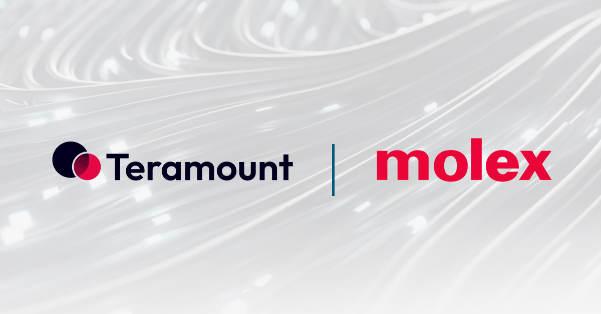
📢 @MolexConnectors has agreed to acquire @TeramountLTD! Together, we’re advancing scalable fiber-to-chip solutions to power AI and hyperscale data centers. Excited for what’s ahead! pulse.ly/0rxevghqiq
#CoPackagedOptics #Photonics #AI #Datacenter #Molex #Teramount
2
1,193

Mar 21
Credo Technology $CRDO is not just a copper story.
It sits at the center of AI data movement.
Rack inside, copper still matters.
Rack to rack, optics grows.
Longer reach, optics grows even more.
But in both worlds, signal integrity still matters. That is where Credo wins.
SerDes, DSP, AEC, optical interconnect.
This is not a one-product company.
This is a picks-and-shovels AI connectivity company.
The market is slowly realizing a simple truth:
No clean data flow, no AI scale.
Nvidia sells compute.
Micron sells memory.
Credo helps move the data between them.
That is why I think $CRDO can become one of the biggest winners of the AI infrastructure cycle.
#CRDO #Credo #AI #ArtificialIntelligence #Semiconductors #Networking #Optics #CPO #CoPackagedOptics #SerDes #DSP #AEC #Datacenter #Hyperscalers #Nvidia #Micron #Broadcom #Marvell #Lumentum #Coherent #AIInfrastructure #TechStocks #GrowthStocks #Borsa #Hisse #Yatırım #Finans #WallStreet #Nasdaq #StockMarket
2
3
11
894

While it’s not inherently low power, CPO offers extremely low energy consumption per transmitted bit — a crucial metric for data center efficiency. semiengineering.com/cpo-is-e…
#CPO #copackagedoptics #datacenters #AIdatacenters
2
2
12
6,435
Good positioning. Silicon Photonics and CoPackagedOptics is the future.
1
1
234

Feb 24
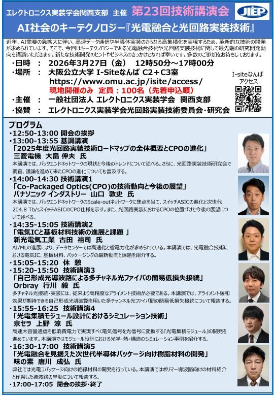
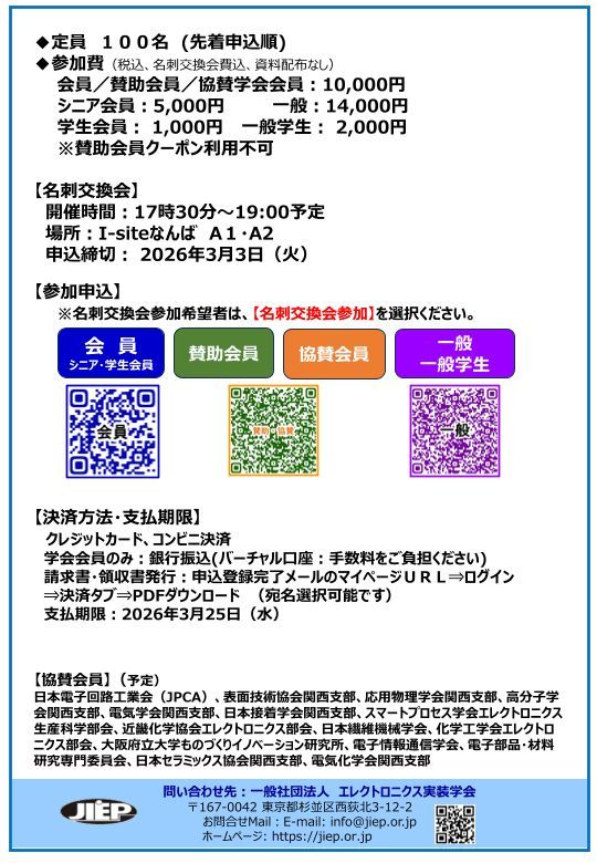
3月27日(金)12時50分~17時00に、エレクトロニクス実装学会 #JIEP 関西支部が第23回技術講演会「AI社会のキーテクノロジー『光電融合と光回路実装技術』」を開催。講演6件。
講演会後に名刺交換会。大阪市浪速区・大阪公立大学I-Siteなんばにて。詳細は buff.ly/GH5c1b1 に。
#Seminar #CPO #CoPackagedOptics #OpticalPackaging
1
3
660

Feb 21
I like Optics and Si Photonics. It won't be as massive as memory or in close proximity to the GPU itself but it has a place in the AI build-out, between servers. It's not a brand new product per se like HBM but AI infra needs them more. $TSM is enabling CoPackagedOptics CPO with their COUPE platform. I like it. too.
3
355
[English easy version: OFC 2026 preview]
"AI chips run too hot. So the laser got kicked out. And that turned out to be the best thing that could have happened."
The defining keyword in optical communications for 2026 is ELSFP — the External Laser Small Form-Factor Pluggable. The principle, stripped of jargon, is straightforward: remove the thermally sensitive laser from the furnace sitting next to the switch ASIC and relocate it to the coolest, most accessible part of the system — the front panel.
Here is why this architectural shift represents a structural moat for InP laser vendors — in four points.
1. The Root Problem: You Cannot Put a Candle Next to a Blast Furnace
CPO (Co-Packaged Optics) bonds the optical engine directly to the switch ASIC to minimize electrical interconnect length and reduce power consumption. The problem is that switch ASICs are blast furnaces — Broadcom Tomahawk 5-class chips dissipate 600–900 W. Lasers are candles — precision devices acutely sensitive to thermal stress.
Placing an InP DFB laser inside the same package produces two failure modes:
Wavelength drift (~0.1 nm/°C): At high temperatures, the laser's emission frequency wanders into adjacent WDM channels, causing inter-channel crosstalk
Sudden death: Failure mechanisms such as facet degradation and Dark Line Defect (DLD) propagation give almost no advance warning — and a laser failure co-packaged with the switch ASIC takes the entire fabric down with it
2. The Fix: ELSFP as an External Power Station
The OIF's conclusion was elegant in its simplicity: decouple the laser entirely and plug it into the front panel — the coldest, most serviceable real estate in the system.
The laser now lives outside the chip package, inserted into the front faceplate of the rack unit like a battery into a device. When it fails, no system shutdown is required. The module is hot-swapped in isolation, and the switch fabric continues operating — a fundamental change in serviceability that hyperscalers require before committing to CPO at scale.
3. Why This Is Structurally Bullish for InP
The long-running narrative — "Silicon Photonics is rising, so InP is dying" — was always wrong. ELSFP makes that explicit.
Silicon is an excellent passive optical medium. It routes light efficiently and integrates cleanly with CMOS processes. But silicon cannot generate light — indirect bandgap physics makes room-temperature CW lasing structurally impossible.
The laser that has been moved outside the package now has a harder job than ever. A single ELSFP must supply CW light to 8–16 SiPh optical engines simultaneously, demanding output powers above 24 dBm (>250 mW) with single-mode operation, narrow linewidth, and guaranteed performance at 50°C. The only material system capable of meeting all four requirements simultaneously is InP — via DFB or MOPA architectures refined over decades of compound semiconductor process development.
The role transformation is decisive: InP went from being one component inside a transceiver module to being the standardized energy infrastructure for the entire CPO ecosystem. The more aggressively SiPh scales, the more indispensable the InP light source becomes.
4. What Investors Should Watch at OFC 2026
When the ELSFP live demo goes live at OFC 2026, two questions are all that matter:
Who is building the power plant?
The vendors with the deepest InP vertical integration — Lumentum (US) and Furukawa (Japan, PCE 14.3% at 55°C demonstrated) — are the current frontrunners. SiPh fabless companies have no path around sourcing the laser externally. This dependency is not temporary; it is structural.
Has the single point of failure been solved?
One ELSFP feeding eight engines is one failure away from eight simultaneous outages. The companies that ship credible 1 1 redundancy and optical bypass protection are the ones serious about production deployment. This is the technical question that separates a lab demonstration from a hyperscaler-grade product.
[One-Line Summary]
InP lasers were not evicted. They incorporated as an independent, monopoly energy supplier.
The more road Silicon Photonics paves, the more valuable the high-performance fuel — the InP laser — required to drive on it. OFC 2026 is the year that symbiosis hardens into a standard.
#CoPackagedOptics #CPO #ELSFP #SiliconPhotonics #InP #OpticalInterconnects
#OFC2026 #Photonics #DatacenterNetworking #AINetworking #OpticalNetworking #HighPowerLasers #ExternalLaser #OIF
1
2
467